Table of Contents
Advertisement
Quick Links
Advertisement
Table of Contents

Related Manuals for Icom IP501M


Summary of Contents for Icom IP501M
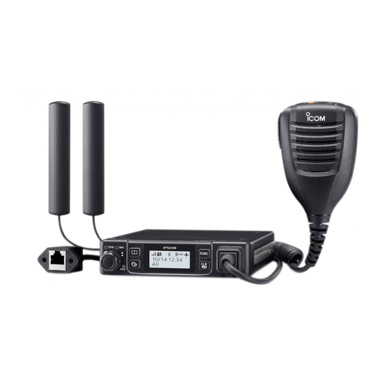
- Page 1 SERVICE MANUAL IP ADVANCED RADIO SYSTEM IP501M S-15606XZ-C1 September 2019...
- Page 2 Addresses are provided on the inside back cover for your convenience. Icom, Icom Inc. and the Icom logo are registered trademarks of Icom Incorporated (Japan) in Japan, the United States, the United Kingdom, Germany, France, Spain, Russia, Australia, New Zealand, and/or other countries.
-
Page 3: Table Of Contents
TABLE OF CONTENTS SECTION 1 SPECIFICATIONS SECTION 2 INSIDE VIEWS SECTION 3 DISASSEMBLY INSTRUCTIONS SECTION 4 OPTIONAL CABLE INSTALLATION SECTION 5 VERIFICATION PROCEDURE PREPARATION ……………………………………………………………………………………… 5-1 LTE TRANSCEIVER ………………………………………………………………………………… 5-3 AUDIO SYSTEM …………………………………………………………………………………… 5-4 BLUETOOTH UNIT ………………………………………………………………………………… 5-4 GENERAL …………………………………………………………………………………………… 5-5 SECTION 6 PARTS LIST SECTION 7... -
Page 4: Specifications
SECTION 1 SPECIFICATIONS VERSION CORRESPONDING MEASUREMENT STANDARD USA-31 FCC Part 15 Class B/ICES003, FCC Part 15C, FCC Part 22, FCC Part 24, FCC Part 27, PTCRB EN 300 328, EN 303 413, EN 301 489, EN 301 908, EN 55024, EN 55032, EN 62311, EN 62368-1, EXP-41 ECE Regulation No. -
Page 5: Inside Views
SECTION 2 INSIDE VIEWS • FRONT-C UNIT (TOP VIEW) [Address] (S1) LCD (DS101) [FUNC] (S3) [Call History] (S2) [CLR/Lock] (S4) • FRONT-C UNIT (BOTTOM VIEW) FRONT PANEL... - Page 6 • FRONT-D UNIT (TOP VIEW) [MICROPHONE] (J1) [DIAL] (S1) INVERTER (IC101) • FRONT-D UNIT (BOTTOM VIEW) FRONT PANEL OVER CURRENT PROTECT SWITCH INVERTER (IC101) (S2)
- Page 7 • MAIN-A UNIT (TOP VIEW) 1.8 V REGULATOR (IC871) GPS ANTENNA REAL TIME CLOCK MODULE DC POWER CABLE ASSEMBLY (W1: CHASSIS-A UNIT) (IC952) (W2: CHASSIS UNIT) LAN CABLE LTE ANTENNA (MAIN) LTE ANTENNA (SUB) (W3: CHASSIS-A UNIT) (W5: CHASSIS-A UNIT) (W5: CHASSIS-A UNIT) J151 LTE MODULE...
- Page 8 • MAIN-A UNIT (BOTTOM VIEW) REVERSE CONNECT PROTECT POWER ON ETHERNET REFERENCE CLOCK (D851) CONTROL CIRCUIT (X951) 3.3 V REGULATOR DC/DC ENABLE SIM SELECTOR ETHERNET TRANSCEIVER IC (IC951) (IC852) CONTROL CIRCUIT CIRCUIT FLASH ROM 13.8 V DC/DC MAIN-A UNIT J254 J253 (IC104) CONVERTER CIRCUIT...
-
Page 9: Disassembly Instructions
SECTION 3 DISASSEMBLY INSTRUCTIONS 1. REMOVING THE FRONT PANEL 4) Disconnect the Bluetooth cable from the MAIN-A UNIT, 1) Remove the 4 screws, and then the top cover from the and the flat cable from the FRONT-D UNIT, and then chassis. - Page 10 2. REMOVING THE MAIN-A UNIT (CONTINUED) 3. REMOVING THE FRONT-D UNIT 3) Unsolder the 2 points of the DC power cables, and a 1) Remove the dial knob and nut from the front panel. point of the ignition cable. UNSOLDER Dial knob Solder remover...
-
Page 11: Optional Cable Installation
SECTION 4 OPTIONAL CABLE INSTALLATION ║ CAUTION! Optional cable must be installed at only the authorized Icom service centers. ║ The performance capability of the transceiver cannot be guaranteed if the user installs a cable themselves, or has it done at ║... - Page 12 ■ D-SUB 25-PIN (OPC-2407) INTERFACE INFORMATION OPC-2407 D-Sub 25-pin Pin name Description Specification D-Sub 25-pin number No connection Serial communication output. (RS-232) Serial communication input. (RS-232) Serial Request-To-Send (RTS) signal input. (RS-232) Serial Clear-To-Send (CTS) signal output. (RS-232) – No connection Ground terminal for transceiver.
-
Page 13: Verification Procedure
MAIN-A UNIT (Top view) to LTE ANTENNA CONNECTOR (MAIN) J604 J604 J502 J502 to MICROPHONE CONNECTOR to LTE ANTENNA CONNECTOR (SUB) JIG cable 1: IP501M See the illustration shown on page 5-2. JIG cable 2: See the illustration shown on page 5-2. - Page 14 ■ JIG [JIG cable 1] MICROPHONE CONNECTOR (Front view) AC millivoltmeter (1 mV to 5 V) 8..1 + − (MIC) (PTT) to pin 6 to pin 4 (GND) (AFO) to pin 7 to pin 3 33 kΩ Audio generator AC millivoltmeter (300~3000 Hz/1~500 mV) (1 mV to 5 V) + −...
-
Page 15: Lte Transceiver
5-2 LTE TRANSCEIVER PREPARATION • Connect the LTE simulator to both main and sub antenna connectors. VERIFICATION [USA-31]: POINTS 4G band B2 (1.9 GHz band: B2 DL 1960 MHz) B4 (2.1 GHz band: B4 DL 2132.5 MHz) B12 (700 MHz band: B12 DL 737.5 MHz) 3G band B2 (1.9 GHz band: B2 DL 1960 MHz) B5 (850 MHz band: B5 DL 880 MHz) -
Page 16: Audio System
5-3 AUDIO SYSTEM VERIFICATION ITEM SETUP OPERATION VALUE MICROPHONE • Adjust the audio generator's output 6.4~12.8 mV rms 1 • Connect the distortion meter and INPUT LEVEL external speaker to the external level so that the distortion meter ~ Microphone speaker jack. -
Page 17: General
5-5 GENERAL VERIFICATION ITEM SETUP OPERATION VALUE LAN PORT 1 • Connect the LAN connector of • Send a ping command. A ping command transceiver to PC with a LAN cable. response from the transceiver SIM CARD 1 • Insert a SIM card to the SIM card •... -
Page 18: Parts List
SECTION 6 PARTS LIST [MAIN-A UNIT] [MAIN-A UNIT] PART PART DESCRIPTION DESCRIPTION LOCATION LOCATION IC101 1140018760 S.IC STM32H750IBK6 26.3/43.6 Q802 1590004310 S.TRA LDTA114EET1G 21.1/27.0 IC102 1130019340 S.IC IS42S16800F-7BLI 52.9/33.9 Q803 1590004060 S.TRA LDTC114EET1G 8.7/46.8 IC103 1130019340 S.IC IS42S16800F-7BLI 52.8/49.4 Q804 1590004310 S.TRA LDTA114EET1G 6.7/46.8 IC104... - Page 19 [MAIN-A UNIT] [MAIN-A UNIT] PART PART DESCRIPTION DESCRIPTION LOCATION LOCATION R105 7030015970 S.RES RMC1/16S-103JTH (10 k) 23.3/44.9 R426 7030016290 S.RES RMC1/16S-222JTH (2.2 k) 18.7/24.3 R106 7030015520 S.RES RMC1/16JPTP 33.1/49.1 R427 7030016560 S.RES RMC1/16SJPTH 14.3/16.7 R107 7030016260 S.RES RMC1/16S-330JTH (33) 25.2/53.8 R430 7030015520 S.RES RMC1/16JPTP 16.7/26.2...
- Page 20 [MAIN-A UNIT] [MAIN-A UNIT] PART PART DESCRIPTION DESCRIPTION LOCATION LOCATION R720 7030016020 S.RES RMC1/16S-104JTH (100 k) 32.6/20.1 R987 7030015910 S.RES RMC1/16S-101JTH (100) 14.8/89.3 R721 7030016560 S.RES RMC1/16SJPTH 34.7/17.8 R988 7030015910 S.RES RMC1/16S-101JTH (100) 14.8/88.4 R722 7030015970 S.RES RMC1/16S-103JTH (10 k) 29.7/17.0 R989 7030015030 S.RES RMC1/16-151JTP (150)
- Page 21 [MAIN-A UNIT] [MAIN-A UNIT] PART PART DESCRIPTION DESCRIPTION LOCATION LOCATION C221 4030022140 S.CER GRM033B31H102KA12D 40.6/66.5 C611 4030022260 S.CER GRM033R60J105MEA2D 8.9/29.9 C222 4030022140 S.CER GRM033B31H102KA12D 43.8/67.5 C612 4030025420 S.CER GRM033R61A105ME15D 16.4/41.0 C223 4030022140 S.CER GRM033B31H102KA12D 21.9/80.7 C613 4030022160 S.CER GRM033B31A104KE84D 18.1/32.6 C224 4030022140 S.CER GRM033B31H102KA12D 23.6/82.7...
- Page 22 [MAIN-A UNIT] [MAIN-A UNIT] PART PART DESCRIPTION DESCRIPTION LOCATION LOCATION C860 4030022150 S.CER GRM033B31E103KA12D 87.1/57.6 EP101 6910018460 S.BEA MMZ1005Y102C-T 31.3/49.8 C861 4030022640 S.CER 0402N101J500CT 87.6/56.4 EP401 6910018460 S.BEA MMZ1005Y102C-T 15.2/24.8 Eqv. 4030026140 S.CER MG15N101J500CT EP402 6910025230 S.BEA BLM15BD221SN1D 18.7/27.6 C862 4030025370 S.CER GRM033R61C104KE14D 92.7/52.2 EP501...
- Page 23 [FRONT-C UNIT] PART DESCRIPTION LOCATION 1590004090 S.TRA LDTC114YET1G 72.5/6.6 1590004090 S.TRA LDTC114YET1G 13.4/17.5 1590004090 S.TRA LDTC114YET1G 6.0/19.5 1590004090 S.TRA LDTC114YET1G 6.0/17.5 1520001010 S.TRA 2SB1132G-R-AB3-R 83.0/14.7 1590003800 S.TRA KTC811U-GR-RTK/P 84.1/9.2 1590004090 S.TRA LDTC114YET1G 14.9/20.0 1790002170 S.VAR LXES15AAA1-133 23.5/16.4 1790002170 S.VAR LXES15AAA1-133 23.5/6.9 1790002170 S.VAR LXES15AAA1-133 87.7/15.1...
- Page 24 [FRONT-D UNIT] PART DESCRIPTION LOCATION IC100 1130007421 S.IC TC7W14FU (TE12LF) 86.2/4.4 IC101 1130007421 S.IC TC7W14FU (TE12LF) 18.2/9.7 1790002170 S.VAR LXES15AAA1-133 86.3/15.4 1790002170 S.VAR LXES15AAA1-133 93.3/4.4 1790002170 S.VAR LXES15AAA1-133 107.6/10.0 1790002170 S.VAR LXES15AAA1-133 97.4/4.0 1790002170 S.VAR LXES15AAA1-133 99.6/5.2 1790002170 S.VAR LXES15AAA1-133 5.5/18.5 1790002170 S.VAR LXES15AAA1-133 11.1/18.0...
-
Page 25: Mechanical Parts
SECTION 7 MECHANICAL PARTS [CHASSIS-A UNIT] [ACCESSORIES] PART PART DESCRIPTION QTY. DESCRIPTION QTY. 8920001880 CAB-1210 5210000061 FGB 5A PBF (FGB0 125V) 8920003150 CAB-1382 8920003160 CAB-1383 8920003090 CAB-1376 – HM-241 † 8210031920 3589 FRONT PANEL (G) 8900022500 OPC-2414 8310093800 3589 WINDOW PLATE (H) 8930089751 3589 WINDOW SHEET-1 8930093860 3589 2-KEY (J) 6510019510 R2-6... - Page 26 Torque: 0.7 N·m (±0.1 N·m) MP23 (CHASSIS-A)×4 (8810009461) Tighten with: Tighten with: “ICOM Driver (U)” (8960000421) “ICOM Driver (U)” (8960000421) Torque: 1.5 N·m (±0.15 N·m) Torque: 1.5 N·m (±0.15 N·m) W5 (CHASSIS-A) W1 (CHASSIS-A) MOBIL BRACKET ASSEMBLED MP15 (CHASSIS-A) (8920003090)
-
Page 27: Board Layouts
SECTION 8 BOARD LAYOUTS The actual configuration of the PC board can be seen by viewing the top and bottom BOARD LAYOUT pages together. • FRONT-C UNIT (B-8944A/B-9169: TOP VIEW) DS12 DS13 DS10 DS11 The serial numbers of transceivers used this PCB. VERSION SERIAL NUMBERS NUMBER... - Page 28 The actual configuration of the PC board can be seen by viewing the top and bottom BOARD LAYOUT pages together. • FRONT-C UNIT (B-8944A/B-9169: BOTTOM VIEW) LCDDT LCDCL LCDSB RSLCD LCDCS DTM1 DLC_B DLC_R FUNC PROG See the PARTS LIST H/V location on the PARTS LIST for location details.
- Page 29 The actual configuration of the PC board can be seen by viewing the top and bottom BOARD LAYOUT pages together. • FRONT-D UNIT (B-8945A/B-9170: TOP VIEW) R104 R101 R102 C102 R103 C103 C110 LCDDT LCDCL LCDSB The serial numbers of transceivers used this PCB. RSLCD LCDCS VERSION...
- Page 30 The actual configuration of the PC board can be seen by viewing the top and bottom BOARD LAYOUT pages together. • FRONT-D UNIT (B-8945A/B-9170: BOTTOM VIEW) [MICROPHONE] [MICROPHONE] R105 R107 See the PARTS LIST H/V location on the PARTS LIST for location details.
- Page 31 The actual configuration of the PC board can be seen by viewing the top and bottom BOARD LAYOUT pages together. • MAIN-A UNIT (B-8943E/B-9168: TOP VIEW) The serial numbers of transceivers used this PCB. MAIN VERSION R990 R992 SERIAL NUMBERS R989 R991 NUMBER...
- Page 32 The actual configuration of the PC board can be seen by viewing the top and bottom BOARD LAYOUT pages together. • MAIN-A UNIT (B-8943E/B-9168: BOTTOM VIEW) R901 R902 R903 D902 R904 D901 C901 D851 T951 C990 D453 Q455 Q456 FI951 FI952 D455 C457...
-
Page 33: Block Diagram
SECTION 9 BLOCK DIAGRAM FRONT-C UNIT FRONT-D UNIT MAIN-A UNIT EN_A IC100, S1~S4 D1~D4 IC101(2) SEL,PROG,FUNC,PSW SEL,PROG,FUNC,PSW SEL,PROG,FUNC,PSW INVERTER PROTECT LCDCL,LCDDT,LCDCS,RSLCD,LCDSB LCDCL,LCDDT, LCDCL,LCDDT, DLC_B,DLC_R,TLC,RLC,BLC,DTM1 LCDCS,RSLCD,LCDSB LCDCS,RSLCD,LCDSB IC101(1,3) VLA,VLB Q3,Q7,Q8, PUSH EN_A ENCODER INVERTER DS1~DS3, DS6~DS8, DS10~DS13 EN_B LIGHT [MICROPHONE] DLC_B,DLC_R, DLC_B,DLC_R, TLC,RLC, TLC,RLC,... - Page 34 MAIN-A UNIT EN_A EN_A CHASSIS-A UNIT J254 VDD3R6,VDD3R3_CPU VDD3R6 IC251,IC252, D255~D258 Q253,Q256 IC201 VDD3R3_CPU CHASSIS-A UNIT IC802,D802 D851 EXT GPS ANT REVERSE D204 3.3V VDD_INPUT VDD3R3 CONNECT J201 CONNECTOR PROTECT DC/DC PROTECT VDD3R3_SPI SELECTOR BIAS PROTECT DC POWERED VDD3R3_RAM DCDC_EN DCIN VDD3R3_CPU GPS ANNTENA...
-
Page 35: Voltage Diagram
SECTION 10 VOLTAGE DIAGRAM • FRONT-C UNIT 33C (3.3 V) 33C (3.3 V) 8C (8 V) LCDDT LCDCL LCDSB RSLCD LCDDT LCDCS LCDCL DTM4 LCDSB DTM3 DTM2 RSLCD DS101 DTM1 882BH01042 VOUT DLC _ B 33C (3.3 V) DLC _ R FUNC PROG FRONT-D UNIT... - Page 36 • FRONT-D UNIT 33C(3.3V) R101 3.3k IC100 R103 R102 3.3k 3.3k TC7W14FU PROG 33C(3.3V) FUNC 8C (8 V) 33C (3.3 V) FRONT-C UNIT [MICROPHONE] LCDDT M _ +8V M _ +8V MINISMDC050F LCDCL LCDSB RSLCD LCDCS MICE MMZ1608S601A DTM1 DLC _ B DLC _ R RH7NWBPHE20A MAIN-A UNIT (3/6)
- Page 37 • MAIN-A UNIT (1/6) VDD3R3_CPU(3.3V) C998 IC101 L203 R212 YFF31HC2A105MT00 FMC_D2 FMC_A10 FMC_D3 FMC_A11 VDD3R3_SPI(3.3V) VDD5 SPIROM Q202 EP883 LDTC144EE R1027 MMZ1005Y102CT PTTDET IC104 J201 LCDCS FMC_BA0 QSPI_BK1_NCS CLDO R1023 FMC_BA1 QSPI_BK1_IO1 R151 SO/IO1 HOLD#/IO3 GPS ANTENNA CLDI R1024 R108 QSPI_BK1_NCS QSPI_BK1_IO2 R152...
- Page 38 • MAIN-A UNIT (2/6) VDD3R3_CODEC (3.3 V) VDD3R3_CODEC(3.3V) R430 MICIN VDD3R3_CODEC (3.3 V) C_AGND C_DGND 3825 3825 3825 LCDDT LCDDT LCDCS R427 LCDCS LCDCL TX_AF MAIN-A UNIT (3/6) LCDCL AFOF LCDSB AFOF LCDSB AMUT AMUT F_MIC DLC_R F_MIC DLC_R EXTMIC DLC_B EXTMIC DLC_B...
- Page 39 • MAIN-A UNIT (3/6) FRONT-D UNIT J501 [D-Sub CONNECTER] VCC(13.8V) S501 J502 R1033 NANOSMDC016F D_AGND R999 D_TXD R596 D_RXD LCDDT1 LCDDT D_RTS VDD8(8V) VDD3R3(3.3V) D_CTS R595 LCDCL1 LCDCL VDD8_M(8V) MAIN-A UNIT (2/6) R594 EXTMOD LCDSB1 LCDSB DISC Q953 DAFO LDTC114YE R592 Q952 LCDCS1...
- Page 40 • MAIN-A UNIT (4/6) J601 J604 R607 R631 FRONT-D UNIT VDD5(5V) R608 R617 100k IC602 NJU7056F3 C606 C609 R615 L601 C616 R605 BTAF MAIN-A UNIT (3/6) BTAF 120k C607 100P R611 Q603 LDTC114EE 100k BT_KENSA MAIN-A UNIT (1/6) C610 C611 VDD3R3_CPU(3.3V) R603 R609...
- Page 41 • MAIN-A UNIT (5/6) D901 DC INPUT VCC(13.8V) CHASSIS-A UNIT: W2 L1SS400 VDD_INPUT(13.8/26.4V) Q854 C852 TJ15S06M3L L852 L851 L853 YFF31HC2A105MT00 CP15S VDD_INPUT (13.8 V/26.4 V) VDD_INPUT (13.8 V/26.4 V) VDD_INPUT (13.8 V/26.4 V) CP801 100U SLF12575T 100U Q902 VDD3R3(3.3V) LDTC114EE R859 R860 2.2k...
- Page 42 • MAIN-A UNIT (6/6) VDD3R3_CPU(3.3V) Q454 LDTC144EE VDD_INPUT(13.8V/26.4V) D451 IGNITE UDZS9.1B VDD3R3_02(3.3V) D453 DCDC_EN Q456 L1SS400 LDTA114EE VDD3R3_02(3.3V) Q455 LDTC114EE L1SS400 D455 R470 D471 Q461 L1SS400 LDTA144EE Q460 LDTC144EE VDD3R3(3.3V) VDD3R3_02 (3.3 V) D454 L1SS400 IC468 R461 IC469 EN_A R459 EN_B SN74LVC3G14DCTR TC7W125FU...
- Page 43 If you have any inquiries regarding service, contact your distributor. The contact number or E-mail address of your distributor can be found on our website. http://www.icom.co.jp/world/...
- Page 44 S-15606XZ-C1 1-1-32, Kamiminami, Hirano-ku, Osaka 547-0003, Japan © 2019 Icom Inc.