Table of Contents
Advertisement
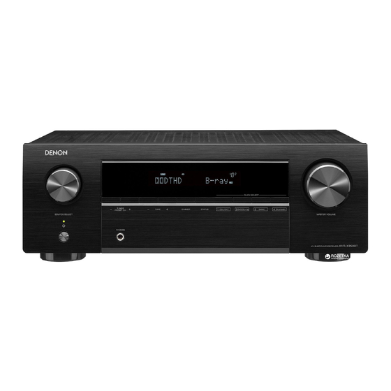
AV SURROUND RECEIVER
AVR-X250BT
• For purposes of improvement, specifications and design are subject to change without notice.
• Please use this service manual when referring to the operating instructions without fail.
• Some illustrations used in this service manual are slightly different from the actual product.
Service Manual
Click here!
On-line service parts list
http://dmedia.dmglobal.com/Document/DocumentDetails/24459
ONLINE PARTS LIST
(P5)
WEB owner's manual
EU:
http://manuals.denon.com/AVRX250BT/EU/EN/index.php
AP:
http://manuals.denon.com/AVRX250BT/AP/ZH/index.php
Upload is planned for the time of a future press release.
BEFORE SERVICING THIS UNIT
ELECTRICAL
MECHANICAL
REPAIR INFORMATION
UPDATING
Confidential
Ver. 1
Advertisement
Table of Contents

Related Manuals for Denon AVR-X250BT


Summary of Contents for Denon AVR-X250BT
- Page 1 Service Manual Ver. 1 AV SURROUND RECEIVER AVR-X250BT Click here! On-line service parts list http://dmedia.dmglobal.com/Document/DocumentDetails/24459 ONLINE PARTS LIST (P5) WEB owner’s manual http://manuals.denon.com/AVRX250BT/EU/EN/index.php http://manuals.denon.com/AVRX250BT/AP/ZH/index.php Upload is planned for the time of a future press release. BEFORE SERVICING THIS UNIT ELECTRICAL...
- Page 2 BEFORE SERVICING THIS UNIT SAFETY PRECAUTIONS NOTE FOR SCHEMATIC DIAGRAM HANDLING THE SEMICONDUCTOR AND OPTICS ONLINE PARTS LIST Accessing the Parts List Searching Part Numbers or Ref. Numbers NOTE FOR PARTS LIST SERIAL NUMBER Serial Number Organization SKU Code of this Unit POST-SERVICE PRECAUTIONS Initializing this Unit...
-
Page 3: Safety Precautions
SAFETY PRECAUTIONS The following items should be checked for continued protection of the customer and the service technician. Leakage current check Before returning the set to the customer, be sure to carry out either (1) a leakage current check or (2) a line to chassis resistance check. If the leakage current exceeds 0.5 milliamps, or if the resistance from chas- sis to either side of the power cord is less than 460 kohms, the set is defective. -
Page 4: Note For Schematic Diagram
NOTE FOR SCHEMATIC DIAGRAM WARNING: Parts indicated by the z mark have critical characteristics. Use ONLY replacement parts recommended by the manufacturer. CAUTION: Before returning the set to the customer, be sure to carry out either (1) a leakage current check or (2) a line to chassis resistance check. -
Page 5: Note For Parts List
ONLINE PARTS LIST Accessing the Parts List Searching Part Numbers or Ref. Numbers (1) Access from the Service Manual You can search a Parts List for part numbers or Ref. numbers. ・ Click the URL link on the cover of the service manual. (1) Enter the part number or Ref. - Page 6 SERIAL NUMBER Serial Number Organization The 14-digit serial number that contains the code of the manufacturing plant and the manufacturing date. 14 digits Factory Manufactured Cumulative Year, month code code serial number The last Month 2digit of year (01 ~ 12) SKU Code of this Unit Product SKU SKU Code...
-
Page 7: Initializing This Unit
POST-SERVICE PRECAUTIONS Initializing this Unit Make sure to initialize this unit after replacing the microcomputer or any peripheral equipment, or the digital PCB. 1. Press the power button to turn off the power. 2. While holding down buttons "TUNER PRESET CH+" and "TUNE +" simultaneously, press the power button to turn on the power. -
Page 8: Schematic Diagrams
ELECTRICAL SCHEMATIC DIAGRAMS LEVEL DIAGRAM SCH01_MCU FRONT ch SCH02_HDMI OSD CENTER ch SCH03_HDMI 4K SURROUND ch SCH04_DSP SUBWOOFER ch SCH05_DIGITAL POWER BLOCK DIAGRAM SCH06_INPUT VOLUME SCH07_AMP ANALOG AUDIO DIAGRAM SCH08_VIDEO, OPTICAL INPUT DIGITAL AUDIO / HDMI DIAGRAM SCH09_BT VIDEO DIAGRAM SCH10_FRONT SCH11_REGULATOR POWER DIAGRAM... - Page 9 SCHEMATIC DIAGRAMS SCH01_MCU CN711 TO BN12B1 TO FRONT B'D FOR UPDATE (MP:OPEN) FOR UPDATE (MP:USE) FFC WAFER/27P/1.25mm FOR UPDATE (AVR-X250BT: ONLY USE) FOR UPDATE (AVR-S540BT/X550BT: USE) AVR-X250BT ONLY FOR AVR-X250BT_BT IOS APP MCU PART CP_SDA CN711 CP_SCL FFC 27P CN716...
- Page 10 SCH02_HDMI OSD HDMI OSD PART R7231 CEC_COM CEC_5V ADV7623_RST INT_TX INT2_RX INT_RX HDMI_SCL HDMI_SDA HDMIOSD_HOLD HDMIOSD_CLK HDMI_RESET <PVDD_1V8> HDMIOSD_CS L7209 36.7mA CB03YTYH600 INT_TX HDMIOSD_MO HDMIOSD_MI <DVDD_1V8> INT2 L7210 332.4mA INT1 CB03YTYH600 X721 HDMI_SCL TO A5 R7246 HDMI_SDA HDMI INPUT-1 R7261 R7262 Q7201 500 ohm...
- Page 11 SCH03_HDMI 4K CEC5V HDMI 4K PART L7301 VDD33 CEC3V3 CB05YTYH221 DGND AVDD33TX L7302 CB05YTYH221 CEC1V1 OPEN AVDD33RX0 TO 2B OSDTX_2+ C7352 L7303 AVDD33RX1 OPEN OSDTX_2- L7309 C7353 CB05YTYH221 OSDTX_1+ AVDD33RX2 OPEN OSDTX_1- C7345 OSDTX_0+ AVDD33RX3 OPEN OSDTX_0- C7346 OSDTX_C+ PVDD33 OPEN OSDTX_C- L7304...
- Page 12 SCH04_DSP DSP PART DIR_INT CODEC_MUTE DSP_MODE_SEL TO 4B TO 5B DIR_CE DIR_RST DIR_MOSI FROM/TO INPUT/VOLUME PART TO DIGITAL POWER PART DIR_CLK DIR_MISO HDMI_SW DSP_CS DSP_SPC1_IRQ DSP_PCP_BSY DSP_RST DSP_MOSI DSP_MISO * Cirrus Recommend DSP_CLK R7424, R7425: 10K-->3.3K Change. TO A2 C7442 100uF/50V +3V3D C7443...
- Page 13 SCH05_DIGITAL POWER TO B2 TO A9 DIGITAL POWER PART TO HDMI 4K PART TO HDMI OSD PART CN751 CN751 YMW025-06R L7501 1.D5.2V CB03YTYH600 L7502 2.D5.2V TO BN601 CB03YTYH600 R7450 L7508 3.M_RESET L7527 CB03YTYH600 L7503 CB03YTYH600 CB03YTYH600 4.D_GND 5.D_GND L7429 R7558 6.MAIN_POWER CB03YTYH600 Q7521...
-
Page 14: Input/Volume Part
* AVR-S540BT/X550BT: JK 772 (2P RCA JACK:CJJ4N121ZD) KRA104S AGND OPEN C7667 OPEN OPEN C7684 OPEN C7699 OPEN C7700 OPEN C7666 C7683 6.AGND * AVR-X250BT: JK 772 (1P RCA JACK:CJJ4M103ZD) KRC104S 100K R7715 DGND R7682 100K R7683 100K R7698 100K R7699 R7714 100K 100K C7629 5.CEN... -
Page 15: M Ain Part
SCH07_AMP M AIN PART Point C1 0.6V Point A 1.10V 53.4V PTC Therm istors D 5101 R5115 R5116 R5126 OPEN 5.6K(1W ) 5.6K(1W ) R5103 R5108 470K PRF18BE471QB5RB/85'C C5103 C5106 33P Q5104 R5117 LEFT FRONT-CH BN505 KT C3114A 4.7(1W ) Q5105 Q5107 13mV... - Page 16 SCH08_VIDEO, OPTICAL INPUT VIDEO/OPTICAL PART NLM 2595 S /W TA B LE(S W 2,5 CO NTRO L) SW 1 SW 3 SW 4 F U N C.IN (14) SW 2 SW 5 (10) R7807 MUTE X (L) 270(1W ) M E DIA PLA YE R CBL/SAT CN781...
- Page 17 SCH09_BT BT PART IC902 BN911 BU33T D 3W G BN911 VOUT 1.+5VA 2.DA_GND IC901 CVIPCM5100APW R 3.USB/BT_R STBY DVDD CPVDD C9005 4.DA_GND 0.1uF DGND CAPP C9007 2.2uF 5.USB/BT_L C9006 LDOO CPGND 0.1uF XSMT CAPM R9012 VNEG TO CN752 OPEN R9001 LRCK OUTL R9015...
-
Page 18: Front Part
2.0m m 3PIN W AFER CN104 TO MAIN TO BN505 2.0m m 9PIN W IRE 2.0m m 3PIN W IRE BN101 CUP12957Z-5 CN104 AVR-X250BT S540BT/X550BT NOT USED BN131 LED OPTION AVR-S640H/AVR-S740H/X1500H USE AVRX1500H E3 OTH ER CUP12957Z-3 D 1012 W H ITE/RED... - Page 19 OPEN OPEN D 3101 AC100V OPEN AVR-S540BT/S640H IC305 AC120~230V OPEN OPEN 932Series 932Series CVIKIA7805BPI AVR-X250BT/X550BT O U T G N D FUSE OPTION F3004 IC301 T 1.25A L 250V CVIK IA7812BPI D 3001 UF4004 O U T F3002 D 3002...
- Page 20 SCH12_SMPS OPTION *OPTION C6002 250V/0.01uF AC100~120V T 2A L 250V *OPTION *OPTION AC220~230V T 1.6A L 250V F6001 D 6001 1N4007 D 6002 1N4007 D 6003 1N4007 D 6004 1N4007 LF602 D 6005 1N4007 E3,K:LF-4ZB-E273H E2,E1C:LF-4ZB-E503H D 6006 1N4007 R6034 C6027 OPEN OPEN...
-
Page 21: Printed Circuit Boards
PRINTED CIRCUIT BOARDS DIGITAL, USB WIRE GUIDE, VIDEO, TUNER, PHONE WIRE GUIDE, FRONT CABLE GUIDE Lead-free Solder When soldering, use the Lead-free Solder (Sn-Ag-Cu). DIGITAL (A SIDE) DIGITAL (B SIDE) DIPPING MEDIA PLAYER CBL/SAT COAX IN MONITOR BD(4K) CBL/SAT(4K) MEDIA PLAYER DVD/Blu-ray GAME(4K) CN716... - Page 22 MAIN MAIN (A SIDE) MAIN (A SIDE)
- Page 23 BT, FRONT, PHONE, STANDBY BT (A SIDE) BT (B SIDE) FRONT (A SIDE) FRONT (B SIDE) CUP12966Z_MP BN912 R9013 L9001 IC901 C9019 C9008 L9002 C9005 R9015 R9001 C9021 C9006 C9022 R9016 R9012 R9002 C9015 R9003 C1073 C9016 R9004 C1074 R9014 R9011 R9005 D1015...
- Page 24 REGULATOR, SMPS REGULATOR (A SIDE) REGULATOR (B SIDE) CUP12910Z-2 FCT1 FCT2 BK301 REGULATOR PART 1A569-V1 MP_STAGE 1.AC_S2 1.AC_S2 2.NC 2.NC 3.RTN_GND C3006 3.RTN_GND 4.NC 4.NC 5.AC_S2 BN301 5.AC_S2 C3024 AC120V F3003/F3004 AC100V J3015 AC220~230V F3001/F3002 C3012 C3007 C3013 C3008 J3004 J3006 C3001 D3003...
- Page 25 LEVEL DIAGRAM FRONT ch AVRS540BT/X550BT/X250BT LEVEL1 DIAG RAM FRO NT ch A/D IN A/D IN D/A O UT ELECTRIC PRE AM P1 PO W ER AM P REV AM P REV AM P VO LUM E AUDIO IN SPK O UT FRO NT NJU72340AFH3 DIG ITAL...
- Page 26 CENTER ch AVRS540BT/X550BT/X250BT LEVEL2 DIAG RAM CENTER ch D/A O UT ELECTRIC PRE AM P1 PO W ER AM P VO LUM E SPK O UT DSP O UT CENTER NJU72340AFH3 CENTER 40dB 40dB 30dB 30dB SPK O UT CS42528 FRO NT DIFF.
- Page 27 SURROUND ch AVRS540BT/X550BT/X250BT LEVEL3 DIAG RAM SURRO UND ch D/A O UT ELECTRIC PRE AM P1 PO W ER AM P VO LUM E SPK O UT DSP O UT SURRO UND NJU72340AFH3 SURRO UND 40dB 40dB 30dB 30dB SPK O UT CS42528 FRO NT DIFF.
- Page 28 SUBWOOFER ch AVRS540BT/X550BT/X250BT LEVEL4 DIAG RAM SUBW O O FER ch D/A O UT SW SUM ELECTRIC REV AM P PRE AM P1 REV AM P VO LUM E SW W O O FER DSP O UT PREO UT NJU72340AFH3 M UTE SUBW O O FER 40dB...
-
Page 29: Block Diagram
MEDIA PLAYER CBL/SAT DA_SW SETUP MIC MIC' DA_SL *AVR-S540BT/X550BT: USED TUNER DA_SR TUNER FM/AM DA_SBL DA_SBR VOL IC NJU72340A AD_FL PRE OUT AD_FR USB/BT_IN(AVR-S540BT/X550BT) MUTE BT_IN(AVR-X250BT) DA_FL DA_FR DA_CEN AVR-X250BT: USED SW1 DA_SW AVR-S540BT/X550BT: USED SW1 & SW2 DA_SL DA_SR... - Page 30 CPVDD: 3V3 *AVR-S540BT/X550BT:USED VDD12:USB1V2 DVDD: 3V3 UART VDD:MCU+3V3 AD_FL AD_FR SN74AHC157PWR MODULE S.FLASH VDD:+1V8H VDDA:+3V3D VDD:USB3V3 DAO_MCK VDDIO:+3V3D DA_FL *AVR-X250BT:USED For GUI HDMI MCLK DA_FR VCC:CEC3V3 S.FLASH DA_CEN For GUI DA_SW VCC:+3V3D VCC:CEC3V3 XOUT DA_SL DA_SR +3V3D TMDS HDMI RX...
- Page 31 VIDEO DIAGRAM AVR-S540BT/X550BT/X250BT VIDEO BLOCK HDMI IN HDMI IN1 (DVD/Blu-ray) ADV7623 HDMI IN2 TRANSCEIVER (MEDIA PLAYER) OSD Block CVDD, DVDD:D1V8H PVDD:D1V8H TXAVDD:D1V8H TXPVDD:D1V8H TXPLVDD:D1V8H X7201 DVDDIO:CEC3V3 28.6363MHz TVDD:CEC3V3 S.FLASH For GUI VCC:CEC3V3 HDMI TX(MN864788) P3 RX HDMI IN HDMI OUT MAIN P0 TX P2 RX...
-
Page 32: Power Diagram
INPUT CURRENT (Ref Volage:5.2V) *DC-DC Effieciency:85% SMPS Total Current : About 3607.786mA(AVR-S540BT/X550BT) 0.005mA SWM5V (HDMI CEC CONTROL/SN74CBT3251PWR) SMPS Total Current : About 2109.901mA(AVR-X250BT) 20mA MCU+5V FRONT LED(CVDBLBJEGJ204L) * TOTAL (5V): 1153.005mA(AVR-S540BT/X550BT) 113mA CS42528(VD), OPTICAL JACK X 2 * TOTAL (5V): 153.005mA(AVR-X250BT) -
Page 33: Wiring Diagram
POWER LED<->FRONT BN101 BN12B BN914 FUNCTION BN912 BN131 CN104 ENCODER BT MODULE POWER BN911 MIC PCB BT PCB LED PCB BT MODULE CN911 H/P PCB BN912 USB & BT PCB * AVR-X250BT: ONLY BT USED *AVR-S540BT/X550BT:MIC & USB & BT USED... - Page 34 SEMICONDUCTORS Only major semiconductors are shown, general semiconductors etc. are omitted to list. The semiconductor which described a detailed drawing in a schematic diagram are omitted to list. STM32F101xC, STM32F101xD, STM32F101xE Pinouts and pin descriptions 1. IC's Pinouts and pin descriptions STM32F101ZE (DIGITAL : IC711) Pass- Figure 3.
- Page 35 Pass- Pass- Pin Name Symbol Function Pin Name Symbol Function Pullup STBY stop Pullup STBY stop Trough STBY Trough STBY 69 PB10 HDMI_RST ADV7623_Reset control 124 PG9 MN864788_SDA MN864788_I2C_SDA C3VPu 70 PB11 HDMI_INT_TX_7623 HDMI INT TX interrupt +3VHPu 125 PG10 EEPROM_SDA M3VPu EEPROM SDA...
- Page 36 ADV7623 Hardware Manual M24128, M24C64, M24C32 Description M24C32WMN6TP (DIGITAL : IC712) Table 6. Function Descriptions Terminal Functions Table 2. Signal names Location Mnemonic Type Description Signal name Function Direction DDCC_SCL Digital Input HDCP slave serial clock port C. DDCC_SCL is a 3.3 V input that is 5 V E0, E1, E2 Chip Enable Input...
- Page 37 ADV7623 Hardware Manual ADV7623 Hardware Manual Location Mnemonic Type Description Location Mnemonic Type Description D in the HDMI interface. TXGND Ground TXAVDD Ground RXD_0+ HDMI Input Digital input channel 0 True of port D in TX0- HDMI Output Differential Output Channel 0 the HDMI interface.
- Page 38 ADV7623 Hardware Manual ADV7623 Hardware Manual Location Mnemonic Type Description Location Mnemonic Type Description MCLK_IN Digital Input Audio Reference Clock. 128 × N × fs with N = 1, 2, 3, or 4. Set to 128 × sampling AP0_OUT Digital Output Audio output port 0.
- Page 39 ADV7623 Hardware Manual ADV7623 Hardware Manual Location Mnemonic Type Description Location Mnemonic Type Description CGND Ground TVDD and CVDD Ground B in the HDMI interface. RXA_C- HDMI Input Digital input clock Complement of port A RXB_1+ HDMI Input Digital input channel 1 true of port B in the in the HDMI interface.
- Page 40 CS497024CVZ (DIGITAL : IC741) EN25Q80B104HIP (DIGITAL : IC742) Table 1. Pin Names Symbol Pin Name DO (DQ NC (DQ WP# (DQ Serial Clock Input DI (DQ DI (DQ Serial Data Input (Data Input Output 0) DO (DQ 8 - LEAD SOP / VSOP / PDIP Serial Data Output (Data Input Output 1) Chip Enable WP# (DQ...
- Page 41 M12L16161A5TG2Q (DIGITAL : IC743) CS42528-CQ (DIGITAL : IC744) Terminal Functions Block diagram Name Input Function System Clock Active on the positive going edge to sample all inputs. Disables or enables device operation by masking or enabling all inputs except Chip Select CLK, CKE and L(U)DQM.
- Page 42 TC74VHC157F/FN/FT/FK TC74VHC157FT (DIGITAL : IC745) Terminal Functions Pin Assignment IEC Logic Symbol (15) SELECT SELECT A S G 1 MUX (11) (10) (14) (12) (13) (top view) Truth Table Inputs Output SELECT X: Don’t care TPS563200 (DIGITAL : IC751 - IC753) TPS562200, TPS563200 DDC (SOT) Package Top View...
-
Page 43: Ordering Information
SCDS019L − MAY 1995 − RE SN74CBT3251 1-OF-8 FET MULTIPLEXER/DEMULTIPLEXER 5-Ω Switch Connection Between Two Ports TTL-Compatible Input Levels D, DB, DBQ, OR PW PACKAGE NJU72340A (DIGITAL : IC761) SN74CBT3251PWR (DIGITAL : IC723) SCDS019L − MAY 1995 − REVISED JANUARY 2004 RGY PACKAGE (TOP VIEW) (TOP VIEW) - Page 44 PCM5100APWR (BT : IC901) TOP268VG (SMPS : IC601) DRAIN (D) CONTROL (C) INTERNAL SUPPLY SHUNT REGULATOR/ ERROR AMPLIFIER SOFT START 5.8 V 4.8 V 5.8 V INTERNAL UV PS(UPPER) COMPARATOR V I (LIMIT) CURRENT LIMIT ADJUST ÷ 16 PS(LOWER) ON/OFF SHUTDOWN/ EXTERNAL CURRENT AUTO-RESTART...
-
Page 45: Pin Connection
ANODE CONNECTION 2. FL DISPLAY 17G(AD3) 18G(AD4) FLD (018BT021GINK) (FRONT : FL101) 8G 9G 10G 11G 12G 13G 14G 15G 16G PIN CONNECTION NOTE 1) F1, F2 ----Filament 2) NP ------No pin 3) DL ------Datum Line 4) NX ------No extend pin 5) LGND ----Logic GND pin 6) PGND ----Power GND pin 7) VH... - Page 46 3. Remote Code Table FORMAT: SHARP / DATA CONSTRUCTION 15bits C14 0 C15 0=NOT INVERTED, 1=INVERTED /REMOTE ID : 1 FORMAT: SHARP / DATA CONSTRUCTION 15bits C14 0 C15 0=NOT INVERTED, 1=INVERTED /REMOTE ID : 1 SYSTEM ADDRESS(C1~C5) : 01000 , EXTENSION BIT(C12,C13) : 11 SYSTEM ADDRESS(C1~C5) : 00110...
- Page 47 REMOTE ID SETTING: GENRE1(*1) GENRE2(*2) ID(*3) ID No. ZONE/DEVICE 21 22 23 24 25 26 27 28 39 40 MAIN ZONE 0 0 1 1 0 0 SHARP&K4-1 TUNER 0 0 1 1 0 0 SHARP&K4-1 AVR-X250BT can receive only ID1 Code.
- Page 48 MAIN ZONE RCKSK0410370 Mute RCKSK0410372 M.VR PRESET1(0dB) REMOTE ID SET: 1 RCKSK0410373 M.VR PRESET2(-20dB) RCKSK0410374 M.VR PRESET3(-40dB) DENON CODE Parity GENRE1 GENRE2 RCKSK0410378 Channel Level 4 5 2 3 0 RCKSK0410383 TEST TONE ON/OFF 25 26 27 28 9 10 11 12 13 14 15 16...
- Page 49 RCKSK0410723 CBL/SAT ANALOG TUNER RCKSK0410725 GAME RCKSK0410726 MEDIA PLAYER REMOTE ID SET: 1 RCKSK0410727 GAME2 DENON CODE Parity GENRE1 GENRE2 RCKSK0410729 4 5 2 3 0 RCKSK0410732 DVD/Blu-ray 25 26 27 28 9 10 11 12 13 14 15 16...
- Page 50 MECHANICAL DISASSEMBLY Flowchart 1. FRONT PANEL ASSY 2. VIDEO PCB 3. DIGITAL PCB 4. MAIN PCB 5. SMPS PCB 6. REGULATOR PCB 7. TRANS EXPLODED VIEW PACKAGING VIEW...
- Page 51 DISASSEMBLY Flowchart • Remove each part following the flow below. • Reassemble the removed parts in the reverse order. • Read "SAFETY PRECAUTIONS" before reassembling the removed parts. • If wire bundles are removed or moved during adjustment or part replacement, reshape the wires after completing the work. Failure to shape the wires correctly may cause problems such as noise. •...
-
Page 52: Front Panel Assy
• The photographs with no shooting direction indicated were taken from the top of the unit. (1) Remove the screws. • Photos of AVR-X250BT E2 are used in this manual. The viewpoint of each photograph (Shooting direction : X) [View from the top] ↓Shooting direction: B↓... -
Page 53: Video Pcb
2. VIDEO PCB 3. DIGITAL PCB Proceeding : TOP COVER → VIDEO PCB Proceeding : TOP COVER → VIDEO PCB → DIGITAL PCB (1) Remove the screws. Remove the FFC. (1) Remove the screws. Remove the connector. Remove the FFC. CN712 CN772 CN713 CN751... -
Page 54: Regulator Pcb
4. MAIN PCB 5. SMPS PCB Proceeding : TOP COVER → VIDEO PCB → DIGITAL PCB → MAIN PCB Proceeding : TOP COVER → SMPS PCB (1) Remove the screws. "EXPLODED VIEW" for instructions on removing the SMPS PCB. 6. REGULATOR PCB Proceeding : TOP COVER →... -
Page 55: Exploded View
EXPLODED VIEW http://dmedia.dmglobal.com/Document/DocumentDetails/24459 Parts List : S6 x2 AVRX250BT EXPLODED VIEW S3 x2 S6 x1 S3 x1 S3 x6 S3 x1 S6 x3 S6 x7 S9 x3 S6 x4 S3 x2 S6 x3 S6 x1 S7 x2 S9 x3 S1 x1 S1 x1 S1 x1 S8 x2... - Page 56 PACKAGING VIEW http://dmedia.dmglobal.com/Document/DocumentDetails/24459 Parts List : UK plug Adaptor...
-
Page 57: Repair Information
REPAIR INFORMATION TROUBLE SHOOTING 1. POWER 2. Analog video 3. HDMI/DVI 4. AUDIO 5. Bluetooth 6. SMPS CLOCK FLOW & WAVE FORM IN DIGITAL BLOCK SPECIAL MODE Special mode setting button 1. Version Display Mode 2. Video Format and Display Language change mode 3. - Page 58 TROUBLE SHOOTING 1. POWER 1.1. The unit does not power on 1.2. Fuse is blown The unit does not power on Blown fuse Does the power indicator on the front panel flash Does the power shut down after several Check for short circuits between the Check the rectifier diode in the in green when the power is turned on? seconds?
-
Page 59: Analog Video
2. Analog video MONITOR OUT (CVBS) output NG Is the power voltage being output correctly? : [C7810 : + side] The power supply circuit is faulty. : [C7811 : - side] Check the pattern between [JK781] and [IC781], Does the signal input to the video amplifier? Is a signal being output from the video amplifier? and then check the Blu-ray/DVD player or the (for SAT/CBL function) - Page 60 3.1. No picture or sound is output (HDMI to HDMI) No picture or sound is output. (8) When using a DENON Blu-ray/DVD player, is the "HDMI" indicator of the fluorescent display lit? Proceed to YES when using a Blu-ray/DVD player produced by other manufactures.
- Page 61 When the Blu-ray/DVD player is connected, check the voltage of the HDMI connector input on (18) the side that the Blu-ray/DVD player is connected to. When using a DENON Blu-ray/DVD player, is the The pattern and circuit from HDMI connector [JK721- Check the waveform of DDC_CLK/DDC_DATA "HDMI"...
- Page 62 3.2. HDMI test point and waveforms DDC_CLK/DDC_DATA/TMDS : Check items (17),(19) DIPPING COAX IN MEDIA PLAYER CBL/SAT MONITOR BD(4K) CBL/SAT(4K) MEDIA PLAYER DVD/Blu-ray GAME(4K) CN716 R7627 CN716 C7702 R7738 T7201 1.RESET C7703 R7655 T7325 T7208 MCU UPDATE 2.MCU+3V3 3.TX R7765 C7621 4.RX R7764...
-
Page 63: Audio Check
4. AUDIO 4.1. AUDIO CHECK No audio output CHECK 1 INPUT SURROUND MODE SOURCE Check the ANALOG AUDIO BLOCK Audio output OK? ANALOG 2CH DIRECT ANALOG CHECK 2 INPUT SURROUND MODE SOURCE Check the DIGITAL AUDIO BLOCK Legacy Audio output OK? COAX or OPT (PCM or DolbyDigital or dts…) CHECK 3... - Page 64 4.2. Power AMP (MAIN PCB) No audio output. Protection is activated. Is the power transistor open or short circuited? Replace the power transistor. 2SB1560 / 2SD2390 Is the emitter resistor of the power transistor open? Replace the emitter resistor. 0.47 Ω Is the base resistor of the power transistor open? Replace the base resistor.
- Page 65 5. Bluetooth 5.1. Cannot establish a Bluetooth connection Check the Bluetooth device being used Is the Bluetooth device compatible with the A2DP Use a device that is A2DP profile compatible. profile? Is the Bluetooth function enabled on the Enable the Bluetooth function and try connecting Bluetooth device? again.
- Page 66 6. SMPS Operation waveform for each part DC 5V is not output. Primary drain After primary side rectification After secondary rectifications (Caution: High voltage, electric shock) (Caution: High voltage, electric shock) Replace the [IC601 : TOP268VG *OPTION Is [IC601 : TOP268VG] damaged? and D6001, D6002, D6003, C6002 250V/0.01uF...
-
Page 67: Clock Flow & Wave Form In Digital Block
CLOCK FLOW & WAVE FORM IN DIGITAL BLOCK WAVE FORM IC721 ADV7623BSDZ HDMI Transceiver (W/GUI) IC731 MN864788 CH1:RXP2 HDMI 1 - 2 HDMI 3 - 5 IC744 CS42528 (DIR+CODEC) RMCK(55) Coaxial1 (49)RXP0 (43)RXP6/GPO6 Optical1 SAI_SCLK(61) (32)DAI2_LRCK IC741 (47)RXP2/GPO2 Optical2 SAI_LRCK(60) (33)DAI2_SCLK CS497024CVZ (34)DAI2_DATA,DSD5... -
Page 68: Special Mode Setting Button
SPECIAL MODE Special mode setting button b No. 1, 2 : While holding down buttons "A" and "B" simultaneously, press the power button to turn on the power. b No. 3, 4 : While the power is on, hold down buttons "A", "B", and "C" for at least 3 seconds . b No. -
Page 69: Version Display Mode
1. Version Display Mode 1.1. Actions 1.4. Error display Version information is displayed when the device is started in this mode. See the table below for descriptions of the displayed errors and countermeasures for these. If multiple errors occur, only one item is displayed. 1.2. - Page 70 2. Video Format and Display Language change mode 2.1. Actions w Select Display Language Select or change "NTSC" or "PAL". Select or change the language. · E2, E1C model Lang.:<ENGLISH> 2.2. Starting up "TUNER PRESET CH +" or "DIMMER" While the power is On, hold down buttons "TUNE -", "TUNE +" and "DIMMER" for at least 3 seconds. ·...
- Page 71 3. Product mode 3-1. Remote Lock mode 1. Actions 3-1.1. Actions Select Remote Lock mode, Tuner Step Change mode, OSD Update mode, Protection History Display This mode prohibits remote control operation. mode. 3-1.2. Starting up 2. Starting up While the power is On, hold down buttons "TUNER PRESET CH +", "TUNE -" and "TUNE +" for at least 3 seconds.
- Page 72 3-2. Tuner Step Change mode (E2 only) 3-3. OSD Update Mode 3-2.1. Actions This is not used during servicing. Do not use. Switches the tuning frequency of the tuner. 3-3.1. Operations 3-2.2. Starting up Exit the OSD Update mode Remove the power plug to exit this mode. While the power is On, hold down buttons "TUNER PRESET CH +", "TUNE -"...
- Page 73 3-4. Protection History Display Mode 3-4.1. Actions (5) Case of Power supply (when the last protection incident is Power protection) This mode enables the unit to record and display the event when the THERMAL, ASO or DC protection is PRT:Power activated.
- Page 74 3-5. PIMG Version Display Mode 4. Front Panel Lock Mode 4.1. Actions This is not used during servicing. Do not use. Switches the panel lock mode. 3-5.1. Operations 4.2. Starting up Exit the PIMG Version Display Mode. Remove the power plug to exit this mode. Press "TUNER PRESET CH -"...
-
Page 75: Adjustment Procedure
IDLING CURRENT Checking Idling Current 1. Preparation MAIN PCB NOTE: Adjusting the idling current when "ECO Mode" is set may damage the Power AMP. (1) Prepare a DC voltmeter. DC Voltmeter (2) Place the unit under normal usage conditions, away from highly ventilated areas such as next to an air conditioning machine or electric fan. - Page 76 UPDATING PROCEDURE AFTER REPLACING THE PCB. PROCEDURE AFTER REPLACING THE U-COM, ETC. FIRMWARE UPDATE PROCEDURE 1. Items necessary for update 2. How to Update...
- Page 77 Implement the update method when the DIGITAL PCB or network module is replaced. DIGITAL PCB Procedure Model Area PCB Name Ref. No. Description Remark after Re- R7113 R7114 placement AVR-X250BT (E2) OPEN DIGITAL IC711 STM32F101ZG SOFTWARE : Main AVR-X250BT (E1C) DIGITAL IC722 EN25QH32B104HIP2B SOFTWARE : GUI ROM See the PCB below.
-
Page 78: Firmware Update Procedure
FIRMWARE UPDATE PROCEDURE 1. Items necessary for update Items necessary for update are as follows. Offered / not Offered Update Type Needed Part for Update Requirement Standard Service Equipment Purchase from D&M Article code Download from SDI Not offered by D&M RS-232C cable 9P (Male), Straight 8U-210100S WRITING KIT... -
Page 79: How To Update
2. How to Update 2.1. Items to Be Prepared 2.3. Start the update. (1) While holding down buttons "TUNER PRESET CH -", "TUNE +" and "DIMMER" simultaneously, (1) Get "AVR-X250BT_Update_Tool.zip" from SDI. (2) Expand the zip file. press the power button to turn on the power. (3) RS-232C cable (9P (Male), Straight). - Page 80 (4) Click "Connect". (6) Click "Load" to load each firmware file. (5) Check the PORT connection destination. ModelName ModelName_DSP_vXXX.bin ModelName_MCU_vXX_XX.bin ModelName_OSD1_vXX_XX.bin ModelName_OSD2_vXXXXXXXX.bin Load File name Load : A ModelName_DSP_vXXX.bin Load : B ModelName_MCU_vXX_XX.bin Load : C ModelName_OSD1_vXX_XX.bin Load : D ModelName_OSD2_vXXXXXXXX.bin (7) A "✓"...
- Page 81 (8) Then start Firmware Update. Updating information. DSP Erasing DSP Updating.. OSD1 Updating.. OSD2 Updating.. MCU Updating.. C:\Users\Desktop\ModelName\ModelName_DSP_vXXX.bin C:\Users\Desktop\ModelName\ModelName_MCU_vXX_XX.bin C:\Users\Desktop\ModelName\ModelName_OSD1_vXX_XX.bin C:\Users\Desktop\ModelName\ModelName_OSD2_vXXXXXXXX.bin (9) After updating the firmware, check the version. "1. Version Display Mode" ---Cautions on Firmware Update--- • Do not turn off the power until updating is completed. •...
- Page 82 Copyright © 2018 D&M Holdings Inc. All Rights Reserved.