Table of Contents
Advertisement
Quick Links
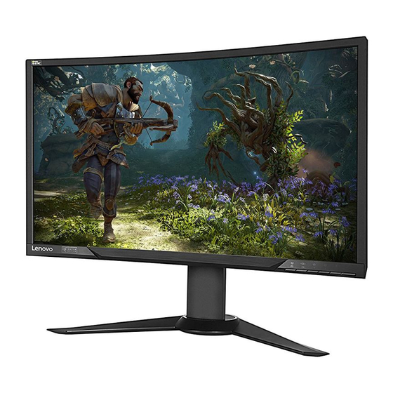
27" LCD Monitor
Service
Service
Service
Description
1. Monitor Specifications ............................................ 4
2. LCD Monitor Description ........................................ 6
3. Operating Instructions ............................................ 7
3.1 General Instructions ............................................. 7
3.2 Monitor Controls ................................................... 7
3.3 OSD Settings ........................................................ 8
4. Input/Output Specification ................................... 12
4.1 Input Signal Connector ....................................... 12
4.2 Factory Preset Display Modes ........................... 13
4.3 Panel Specification ............................................. 14
5. Mechanical Instructions ....................................... 18
6. Block Diagram ....................................................... 23
6.1 Main Board ......................................................... 23
7. Schematic Diagram ............................................... 24
ANY PERSON ATTEMPTING TO SERVICE THIS CHASSIS MUST FAMILIARIZE HIMSELF WITH THE CHASSIS
AND BE AWARE OF THE NECESSARY SAFETY PRECAUTIONS TO BE USED WHEN SERVICING
ELECTRONIC EQUIPMENT CONTAINING HIGH VOLTAGES.
CAUTION: USE A SEPARATE ISOLATION TRANSFOMER FOR THIS UNIT WHEN SERVICING
Table of Contents
Page
Description
7.1 Main Board ......................................................... 24
7.2 Key Board .......................................................... 34
7.3 USB Board ......................................................... 35
8. PCB Layout ............................................................. 39
8.1 Main Board ......................................................... 39
8.2 Key Board .......................................................... 43
8.3 USB Board ......................................................... 44
9. Trouble Shooting ................................................... 49
10. Firmware and DDC Instruction ........................... 53
11. White- Balance, Luminance Adjustment............ 70
12. Monitor Exploded View ....................................... 72
13. BOM List ............................................................... 74
SAFETY NOTICE
1
Lenovo Y27g RE
Horizontal Frequency
53-160 KHz
Page
Advertisement
Table of Contents

Related Manuals for Lenovo Y27g RE


Summary of Contents for Lenovo Y27g RE
-
Page 1: Table Of Contents
27" LCD Monitor Lenovo Y27g RE Service Service Service Horizontal Frequency 53-160 KHz Table of Contents Description Page Description Page 7.1 Main Board ............24 1. Monitor Specifications ..........4 7.2 Key Board ............34 7.3 USB Board ............35 2. - Page 2 Revision List Version Release Date Revision History TPV Model Name Apr.22,2016 Initial release HFFSGQ6KDTLBDC...
- Page 3 Important Safety Notice Proper service and repair is important to the safe, reliable operation of all Lenovo Company Equipment. The service procedures recommended by Lenovo and described in this service manual are effective methods of performing service operations. Some of these service operations require the use of tools specially designed for the purpose.
-
Page 4: Monitor Specifications
1. Monitor Specifications... -
Page 6: Lcd Monitor Description
2. LCD Monitor Description The LCD monitor will contain a main board, a power board, two USB boards and a key board which house the flat panel control logic, brightness control logic and DDC. The power board will provide AC to DC Inverter voltage to drive the backlight of panel and the main board chips each voltage. -
Page 7: Operating Instructions
3. Operating Instructions 3.1 General Instructions Press the power button to turn the monitor on or off. The other control buttons are located at the front of the panel of the monitor. By changing these settings, the picture can be adjusted to your personal preferences. ... -
Page 8: Osd Settings
3.3 OSD Settings... -
Page 12: Input/Output Specification
4. Input/Output Specification 4.1 Input Signal Connector HDMI pins definition: Pin Number Contents Pin Number Contents TMDS Data2+ TMDS Clock Shield TMDS Data2 Shield TMDS Clock– TMDS Data2– TMDS Data1+ Reserved (N.C. on device) TMDS Data1 Shield TMDS Data1– TMDS Data0+ DDC/CEC Ground TMDS Data0 Shield +5 V Power... -
Page 13: Factory Preset Display Modes
4.2 Factory Preset Display Modes... -
Page 14: Panel Specification
4.3 Panel Specification 4.3.1 General Features LTM270HP02is a color active matrix liquid crystal display(LCD) that uses amorphous silicon TFT (Thin Film Transistor) as switching components. This model is composed of a TFT LCD panel, a driver circuit and a back light unit.The resolution of a 27.0”... - Page 15 4.3.3 Optical Characteristics (Ta=25℃, V =12V, fv=60Hz Fdclk=35.3MHz, I =300mA)
- Page 16 4.3.4 Electrical Specification...
- Page 17 Black Light...
-
Page 18: Mechanical Instructions
5. Mechanical Instructions 1. Precaution Please read the precautions as follows to prevent any damages to the LCD Monitor. Make sure all power connection is removed. Be sure that the LCD Monitor is in power off status. Prepare soft cloth and sponge as working platform to place LCD monitor horizontally. - Page 19 2. Appropriate tools Select the appropriate tools for disassembly and re-assembly. Phillips screwdriver spacer screwdriver C/D Disassembly Tool Gloves or soft cloth...
- Page 20 3. Disassembly SOP 1. Remove the stand assy Starting from the back of the monitor, reamove the screws to remove the stand assy. 2. Separated the rear cover and the bezel.
- Page 21 Remove the connectors and tapes Remove the FFC cable and the screws to remove the mainframe. The Panel...
- Page 22 3. Remove the boards Remove screws Remove the connectors of the boards. 4. Separated the bezel and the key board.
-
Page 23: Block Diagram
6. Block Diagram 6.1 Main Board... -
Page 24: Schematic Diagram
7. Schematic Diagram 7.1 Main Board (715G8134M0E000006T) CN401 Female Con LVDS_7_DATA_P4 LVDS_5_DATA_P4 LVDS_7_DATA_N4 LVDS_5_DATA_N4 LVDS_5_DATA_P3 LVDS_7_DATA_P3 LVDS_5_DATA_N3 LVDS_7_DATA_N3 LVDS_7_DATA_P2 LVDS_7_DATA_N2 LVDS_5_DATA_P2 LVDS_5_DATA_N2 LVDS_7_CLK_P LVDS_5_CLK_P LVDS_5_CLK_N LVDS_7_CLK_N LVDS_5_DATA_P1 LVDS_7_DATA_P1 LVDS_5_DATA_N1 LVDS_7_DATA_N1 LVDS_5_DATA_P0 LVDS_7_DATA_P0 MH01 LVDS_5_DATA_N0 LVDS_7_DATA_N0 LVDS_6_DATA_P4 LVDS_4_DATA_P4 LVDS_6_DATA_N4 LVDS_4_DATA_N4 LVDS_4_DATA_P3 LVDS_4_DATA_N3 LVDS_6_DATA_P3 MH01/MH02 f oot print change... - Page 25 Big plane R7012 0R05 1/4W R7015 0R05 1/4W +19V R7017 0R05 1/4W R7001 430K 1% U7001 DC-POWER Input Big plane C7067 C7068 C7069 C7066 220UF 35V 220UF 35V CN7001 +19V C7006 10UF 25V 10UF 25V R7003 Q7104 R7002 R7004 10UF 25V 1.5R 100K 1/16W 5% 10 OHM 1%...
- Page 26 To panel CN1 CN402 To panel CN3 CN404 LVDS_5_DATA_N4 LVDS_5_DATA_P4 LVDS_1_DATA_N4 LVDS_1_DATA_P4 LVDS_5_DATA_N3 LVDS_5_DATA_P3 LVDS_1_DATA_N3 LVDS_1_DATA_P3 LVDS_5_CLK_N LVDS_1_CLK_N LVDS_5_CLK_P LVDS_1_CLK_P LVDS_5_DATA_P2 LVDS_5_DATA_N2 LVDS_1_DATA_P2 LVDS_1_DATA_N2 LVDS_5_DATA_N1 LVDS_5_DATA_P1 LVDS_1_DATA_N1 LVDS_1_DATA_P1 LVDS_5_DATA_N0 LVDS_5_DATA_P0 LVDS_1_DATA_N0 LVDS_1_DATA_P0 LVDS_4_DATA_N4 LVDS_4_DATA_P4 LVDS_0_DATA_N4 LVDS_0_DATA_P4 LVDS_4_DATA_N3 LVDS_4_DATA_P3 LVDS_0_DATA_N3 LVDS_0_DATA_P3 LVDS_4_CLK_N LVDS_0_CLK_N LVDS_4_CLK_P...
- Page 27 DCP_FB +19V C7043 R7047 +19V 2,15 10K 1/16W NC56pF 50V U7005 R7048 140K 1% Panel_VCC APW7089KAI-TRG R7049 +19V_IN_Panel NC/0R05 OHM DCP_COM R7050 L7004 UGND COMP DC_Panel_EN Panel_P 100K 1/16W 5% C7044 22UH DCP_VCC C7045 C7046 C7047 C7048 100UF 25V 1uF 25V C7050 C7051 C7049...
- Page 28 L801 33UH FB802 +19V D801 SR3100-MK18 +19V C801 BEAD R801 220UF 35V C802 R802 C803 100N 50V Q801 100 OHM 1/4W 10 OHM 1% 470NF 50V R803 PA110BDA 10K 1/10W 5% R804 VBLCTRL R837 C804 C807 R824 33UF 100V 330KOHM +-1% 1/4W R806 R805 C805...
- Page 29 EE_3V3_SDA 8,15,16 EE_2V5 EE_3V3_SCL 8,15,16 R117 R118 R119 C127 4.7K1/16W 4.7K1/16W NC/1K 1/16W 5% 220N 10V U107 R146 0R05 OHM R147 0R05 OHM EE_SCL R148 0R05 OHM R122 EE_SDA 2.2K1/16W M24C16-RMN6TP EEPROM_WP_HDCP R120 U109 f oot print change t o: 0R05 OHM SOP8-P-6_2-1_27 f or A llegro...
- Page 30 CN418 +2.5V_UC MONITOR_LED_G_BUFF R433 0R05 1/10W modif y 470 R404 R434 NC/0R05 1/10W 200R 1/10W 5% CONN PNL_LEDGD R405 R401 R402 R403 20K 1/16W 20K 1/16W 20K 1/16W Reserve CN408 - 20131209 CN406 CN408 Q401 2.5V 1.71V MONITOR_LED_GD AO3401A BUTTONS_PIN_4 R425 100R 1/16W 5% KEY 1...
- Page 31 C608 C620 1uF 25V 1uF 25V HPN_JCK_HPS CN710 CONN +5V_AUDIO FB610 HPN_JCK_HPR_J NC/120R 0.3A PLACE CLOSE T O LM 49 450 HPN_JCK_HPL_J +5V_AUDIO ZD606 PLA CE CL OS E T O L M 4 945 0 NC/RLZ5.6B C650 LM49450_LSVDD NC/100N 16V L601 0.400 22uH...
- Page 32 U101 U102 AOZ8804DI AOZ8804DI CN101 SHELL1 SHELL3 DP_LNK_RX_DPCONN_N3 ML_ Lane 3(n) 90DIFF_NETCLASS1 DP_LNK_RX_DPCONN_P3 90DIFF_NETCLASS1 ML_ Lane 3(p) DP_LNK_RX_DPCONN_N2 ML_ Lane 2(n) 90DIFF_NETCLASS1 DP_LNK_RX_DPCONN_P2 ML_ Lane 2(p) 90DIFF_NETCLASS1 DP_LNK_RX_DPCONN_N1 ML_ Lane 1(n) 90DIFF_NETCLASS1 DP_LNK_RX_DPCONN_P1 90DIFF_NETCLASS1 ML_ Lane 1(p) ML_ Lane 0(n) DP_LNK_RX_DPCONN_N0 90DIFF_NETCLASS1 ML_ Lane 0(p)
- Page 33 1V2_DPIN 3V3_DPIN U509 0.5A HDMI_5V DVDD1V2_HDMI_IN 0.400 FB502 60R 0.6A C511 C512 C513 C514 C515 R535 R536 R537 R507 R508 10uF 16V 0.47UF 10V 100NF 16V 100NF 16V 10PF 50V STD P2600_U ART_5V_TX 0R05 OHM NC/0R05 OHM C504 C505 C506 C507 C508 C509...
-
Page 34: Key Board
7.2 Key Board (715G8146K01000004Y) LED001 Amber White 12-22A/Y 2T7D-C30/2C 換新的FFC 料號 CN001 CABLE KEY 1 R001 2K 1/10W 5% KEY 2 POWER_KEY # DC Power R002 100R 1/10W 5% LED_G White LED_R Amber R005 100R 1/10W 5% R003 2K 1/10W 5% R004 1K 1/10W 5% R006... -
Page 35: Usb Board
7.3 USB Board (715G8165T0C000005Y) I(Max)≠500mA C7182 close to pin85 DV12 AV12 +3.3V_USB Differential trace, space, trace is 8, 7, 8 (mil). C7183 close to C7182 DV12 AV12 +3.3V_USB TXP_UP L7008 SSTX0+ Ground gap > 20mil. Impedance is 90ohm. FB7037 Differential pair mismatch < 5mil. TXN_UP SSTX0- U7010... - Page 36 +3.3V_LED Add CHROMA LIGHT EN PIN Debug port I2C for Chroma 20160113. +3.3V_LED CN7103 Debug connect change +3.3V_LED +3.3V_LED lighting control GPIO 5V_LED 5V_LED to 5 pin 20151123. CHROMA_LIGHTING_EN# C7101 C7102 H: OFF 0.1UF 16V 0.1UF 16V +3.3V_LED 5V_LED +3.3V_LED CN7103 L: ON DGND...
- Page 37 (715G8166T0B000005K) DGND Add L7025/L7026 ; FB7049/FB7050 ; C7094-C7097 for EMI 3.0(DOWN3) solution 20160113. CN7006 +5V_DP3_1 CONN +5V_DP3_1 +5V_DP3_2 +5V_DP3_1 U7001 CN7007 3.0(Side) USBHP3-_1 USBHP3+_1 FB7049 I/O1 I/O6 SSRX3- SSRX3+ SSRX3- I/O2 I/O5 L7025 C7098 USBHP3- USBHP3-_1 SSTX3- SSTX3+ SSRX3+ I/O3 I/O4 +5V_DP3_1 USBHP3-_1...
- Page 38 AUDIO OUTPUT CN602 AUDIO_SD VOLUME AUDIO_MUTE +5V_AUDIO AUDIO_SOUTR +5V_AUDIO AUDIO_SOUTL 5V_AUDIO +5V_AUDIO R612 R602 FB606 CONN 10K 1/10W 5% 300R 4A +5V_AUDIO R606 R607 VOLUME ZD601 C601 C602 C603 D601 C609 R608 100R 1/16W 5% NC/RLZ5.6B LL4148 10UF 25V NC/1K 1/10W 5% R611 100N 16V 10uF 16V...
-
Page 39: Pcb Layout
8. PCB Layout 8.1 Main Board (715G8134M0E000006T) -
Page 43: Key Board
8.2 Key Board (715G8146K01000004Y) -
Page 44: Usb Board
8.3 USB Board (715G8165T0C000005Y) - Page 48 (715G8166T0B000005K)
-
Page 49: Trouble Shooting
9. Trouble Shooting 1. No Power No power Check power cable is Re-plug the power cable tightened? Check Power “On/Off” Turn on the Power “On/Off” switch is “On”? Check the LED Check the AC power indicate is OK? Replace the power board and check connections Replace main board and check connections Replace key board and check connections... - Page 50 2. No Video (LED Green) No Video (LED Green) Press the power Replace the main board button is OK? Replace the power The end board and connection Replace the main The end board and connection Check the FFC cable Replace the FFC cable or panel or panel Replace the key board...
- Page 51 3. DIM DIM (image overlap, focus or flicker) Reset in factory mode The end Set to the optimal The end frequency, select the recommended frequency Readjust the phase and The end pixel clock in the user Pull out signal cable Check the signal cable and check “Self Test and the PC...
- Page 52 4. Color is not optimal Color is not optimal Color shift Miss color Reset the factory mode Replace the signal cable In the user mode, set the” color settings” until customer satisfy The end Pull out the signal cable and check the screen color display is normal? Replace the signal cable or PC Replace the main board...
-
Page 53: Firmware And Ddc Instruction
10. Firmware and DDC Instruction 10.1 F/W Upgrade SOP 1.Materials list MSP430tool(driver) usb-blaster(driver) MSP430 software usb-blaster software Monitor usb cable MSP430 tool usb-blaster tool 2.Install driver When insert the msp430 tool and usb-blaster tool to PC, you need to install the driver. 3. - Page 54 3.1.2 TI micro-controllers FW update This chapter describes how to flash new code into the two TI-MSP430 micro-controllers on the NVIDIA G-SYNC module and base board. These two micro-controllers take care of handling the button presses and the LED control of the monitor.
- Page 55 3.1.4 Required Software In order to load the binary code into the flash memories for the micro-controllers, we use the Elpotronic FET-Pro430 Lite software. This software is free to use and can be downloaded from http://www.elprotronic.com/download.html. 3.1.5 Updating the base board micro-controller 3.1.6 Cable Connections Connect the cable that came with the TI MSP-FET430UIF in the way indicated in the picture above.
- Page 56 3.1.9Selecting the correct communication protocol Click on the “setup->connection/device reset” menu, and the following popup should come up: Make sure that the “Spy Bi Wire” communication with Target Devices is selected(and not “JTAG”). All other options should already be correct. Click “ok” to apply and close popup. 3.1.10 Selecting the code file Now click the “Open code file”...
- Page 58 3.1.11 Flash the code Now click the “AUTO PROG” Button. After finished, the screen should look like this:...
- Page 59 4. G-SYNC module FW update 4.1 G-SYNC module FW update This chapter describes how to flash Bitstream, Bitmaps Files(.bin),OSD control FW(.elf) and Panel profiles into G-SYNC module. 4.2 Required Hardware G-SYNC monitor with power supply USB blaster To download the program code into the FPGA, we use the Terasic USB Blaster: http://www.terasic.com.tw/cgi-bin/page/archive.pl?Language=English The USB port of the blaster is connected to the development computer, and the header cable is connected to the header on the monitor.
- Page 60 Installing the USB Blaster Device Driver 4.3 Required Software Download the Nios II programming environment as part of the Altera Quartus II Design Suite from: https://www.altera.com/download/sw/dnl-sw-index.jsp. Select the Quartus II subscription Package(we only use the Nios II programming environment component of the suite-the “Paid license required” message can be ignored) 4.4 Flash .bin/.elf/panel profiles Step1.
- Page 61 Step3: keeping command line window, and key-in the folder path based on your folder location. In this sample, through below way going to Lenovo_Y27g_SVT_V08 Step4: executed ./flash_packet_section.sh to flash .bin/.elf and panel profile.
- Page 62 Step5: the script starting to program .bin/.elf and panel profile. Program.bin Program.elf Program. panel profile...
- Page 63 Q&A: 1. Which conditions shall update FW? Totally, Lenovo_Y27g_SVT_V08 having 6 parts FW combination to become G-SYNC model. a. Bit-stream The modules ship pre-programmed with Rel7, which is the exact same RTL and DP CPU code as is in Rel8. The RTL and DP CPU code hasn’t changed since Rel7. So this part we don’t need to flash it unless NV updates RTL or DP CPU code.
- Page 64 10.2 EDID writing SOP by VGA single port ISP JIG: 715GT089-C hdmi cable USB cable TPV P/N: 089G183GAA501 TPV P/N: 089G1758 X MSTAR driver Monitor USB port driver ISP tool EDID...
- Page 65 4.1. Change the EDID files name as below rule. HDMI EDID WH.dat 4.2. Copy these files to one folder named as LENOVO Y27g which must contains “config.ini” file. 4.3. Copy LENOVO Y27g to DDC folder and put DDC and ISP tool together.
- Page 66 4.4. Setting the Config.ini as below 4.5 You should open the factory menu before writing EDID. (1)Press the key button 6436 to enter the factory menu; (2)Don’t close the factory menu while writing EDID. ⑥ ⑤ ④ ③ ② ①...
- Page 67 5. Run the ISP tool 5.1. Double-click the icon to open the tool. 5.2. Select the EDID folder.
- Page 68 5.3 Tick the “Multi-interface”& “HDMI”, then click “Debug Information”; type in the 8 digit S/N 5.4 Start to writing. Click “write EDID” to start writing. When The green “PASS” appear, the process is finished.
- Page 69 6. Troubleshooting. 6.1. Can’t write! (1) AC on the monitor and turn on it.(Restart the monitor) (2)Take apart the monitor and connect the 7pin of EEPROM to GND to diable write protection then write EDID one by one. (3) Set the Burn in on last to try again.
-
Page 70: White- Balance, Luminance Adjustment
Y value and use “ID” key to modify the TEXT description Following is the procedure to do white-balance adjust . Enter into the Factory mode of Lenovo Y27g RE: DC off, press the " left + MENU", and then DC on, you can enter into the factory mode. - Page 71 D. Adjust sRGB color-temperature 1. Switch the chroma-7120 to RGB-Mode (with press “MODE” button) 2. Switch the MEM.channel to Channel 10 (with up or down arrow on chroma 7120) 3. The LCD-indicator on chroma 7120 will show x = 313 ± 20, y = 329 ± 20 4.
-
Page 72: Monitor Exploded View
12. Monitor Exploded View... - Page 73 Item Description BEZEL L27WR-Ylh7-p7 COVER_CLOCK_FRONT KEY BOARD LENS DECO_BEZEL L27WR-Ylh7-p7 COVER_CLOCK_FRONT LCD LTM270HP02 M01 SZ SEC MAIN BOARD-CBPCFGQL1Q1 USB BOARD MAINFRAME Item Part No. Description REAR_COVER L27WR-Ylh7-p7 0M1G1030 6120 SCREW M3 6(MAIN BOARD/MAINFRAME) HINGE ASS'Y 0M1G1030 6120 SCREW M3 6(USB BOARD/MAINFRAME) USB BOARD 0M1G 930 4120 SCREW 3x4 (MAINFRAME/PANEL)
-
Page 74: Bom List
395GH20016XM003000 HARNESS 16P(2004)-16P(2004) 100mm ECN404/405 395GLM5132R5030000 LVDS CABLE 51P-30P+32P 280/280mm 2nd Source ECN404/405 395GLM5132X5030000 LVDS CABLE 51P-30P+32P 280/280mm 708GF1146080CPQ1WW LENOVO 40(512) WW 050G060000100W00JI STRAP Q45G 77 4 PE PACKING Q45G 77 5 PE PACKING Q50G 4 10 TIE (Y1900221) Q52G13010120HF0ADG... - Page 75 SMTC-U107 100GLASG004NT1 MCU ASSY-356G1133056015 CBP-ECN401 100GLASG100NT1 MCU ASSY CN401 317GAAMB190NVI MAIN BOARD 900-12324-0020-000 CBPCFGQL1Q1 CONVERSION BOARD Y27 GAMING 715G8134-M0 H40G 45762429A LABEL J102 033G3802 5B Y CONNECTOR 5P 2.0 CN802 033G3802 6B Y CONN 6PIN 2.0 C150 067G204V680 4K CAP CS 68UF 20% 25V 8*11 C804 067G415R479 9K EC 4.7UF 20% 100V ED 8*12...
- Page 76 Q7002 057G 417511 MMBT3904 Q402 057G 417511 MMBT3904 Q7105 057G 417512 MMBT3906 Q7003 057G 417518 TRA LMBT3904LT1G 200mA/40V SOT-23 LRC Q404 057G 417518 TRA LMBT3904LT1G 200mA/40V SOT-23 LRC Q7105 057G 417518 TRA LMBT3904LT1G 200mA/40V SOT-23 LRC Q402 057G 417518 TRA LMBT3904LT1G 200mA/40V SOT-23 LRC Q7002 057G 417518 TRA LMBT3904LT1G 200mA/40V SOT-23 LRC...
- Page 77 R419 061G0402000 JT RST 0402 0.05R MAX 1/16W - R584 061G0402000 JT RST 0402 0.05R MAX 1/16W - R448 061G0402000 JT RST 0402 0.05R MAX 1/16W - R447 061G0402000 JT RST 0402 0.05R MAX 1/16W - R109 061G0402000 JT RST 0402 0.05R MAX 1/16W - R7070 061G0402000 JT RST 0402 0.05R MAX 1/16W -...
- Page 78 R578 061G0402000 JY RST CHIPR MAX 0R05 OHM 1/16W YAGEO R601 061G0402000 JY RST CHIPR MAX 0R05 OHM 1/16W YAGEO R121 061G0402000 JY RST CHIPR MAX 0R05 OHM 1/16W YAGEO R604 061G0402000 JY RST CHIPR MAX 0R05 OHM 1/16W YAGEO R507 061G0402000 JY RST CHIPR MAX 0R05 OHM 1/16W YAGEO...
- Page 79 R581 061G0402101 JY RST CHIPR 100 OHM +-5% 1/16W YAGEO R426 061G0402101 JY RST CHIPR 100 OHM +-5% 1/16W YAGEO R427 061G0402101 JY RST CHIPR 100 OHM +-5% 1/16W YAGEO R505 061G0402102 JF RST CHIPR 1KOHM +-5% 1/16W FENGHUA R573 061G0402102 JF RST CHIPR 1KOHM +-5% 1/16W FENGHUA R613...
- Page 80 R408 061G0402103 JY RST CHIPR 10KOHM +-5% 1/16W YAGEO R7034 061G0402103 JY RST CHIPR 10KOHM +-5% 1/16W YAGEO R113 061G0402103 JY RST CHIPR 10KOHM +-5% 1/16W YAGEO R7250 061G0402103 JY RST CHIPR 10KOHM +-5% 1/16W YAGEO R536 061G0402103 JY RST CHIPR 10KOHM +-5% 1/16W YAGEO R7036 061G0402103 JY RST CHIPR 10KOHM +-5% 1/16W YAGEO...
- Page 81 R7002 061G0402104 JY RST CHIPR 100KOHM +-5% 1/16W YAGEO R452 061G0402104 JY RST CHIPR 100KOHM +-5% 1/16W YAGEO R7050 061G0402104 JY RST CHIPR 100KOHM +-5% 1/16W YAGEO R546 061G0402105 JF RST CHIPR 1MOHM 5% 1/16W FENGHUA R545 061G0402105 JF RST CHIPR 1MOHM 5% 1/16W FENGHUA R112 061G0402105 JF RST CHIPR 1MOHM 5% 1/16W FENGHUA...
- Page 82 R403 061G04022002FF RST CHIPR 20KOHM +-1% 1/16W FENGHUA R7006 061G04022002FF RST CHIPR 20KOHM +-1% 1/16W FENGHUA R7011 061G04022002FY RST CHIP 20K 1/16W 1% YAGEO R7014 061G04022002FY RST CHIP 20K 1/16W 1% YAGEO R402 061G04022002FY RST CHIP 20K 1/16W 1% YAGEO R403 061G04022002FY RST CHIP 20K 1/16W 1% YAGEO...
- Page 83 R531 061G0402302 JF RST 0402 3K 5% 1/16W R531 061G0402302 JT RST 0402 3K 5% 1/16W R7116 061G0402303 JF RST 0402 30K 5% 1/16W R7116 061G0402303 JT RST CHIP R 30Kohm 1/16W +/-5% TZAI YUAN R7029 061G04023302FF RST 0402 33K 1% 1/16W FENGHUA R7029 061G04023302FY RST CHIP 33K 1/16W 1%...
- Page 84 R554 061G0402472 JY RST 0402 4.7K 5% 1/16W RC0402JR-074K7L R556 061G0402472 JY RST 0402 4.7K 5% 1/16W RC0402JR-074K7L R553 061G0402472 JY RST 0402 4.7K 5% 1/16W RC0402JR-074K7L R557 061G0402472 JY RST 0402 4.7K 5% 1/16W RC0402JR-074K7L R414 061G0402472 JY RST 0402 4.7K 5% 1/16W RC0402JR-074K7L R409 061G0402473 JT RST CHIP 47K 1/16W 5% TZAI YUAN...
- Page 85 R7068 061G0603104 JT RST CHIP 100K 1/10W 5% TZAI YUAN R7040 061G0603104 JT RST CHIP 100K 1/10W 5% TZAI YUAN R7040 061G0603104 JY RST CHIPR 100KOHM 1/10W YAGEO R7068 061G0603104 JY RST CHIPR 100KOHM 1/10W YAGEO R7026 061G0603104 JY RST CHIPR 100KOHM 1/10W YAGEO R819 061G0603109 JF RST 0603 1R 5% 1/10W -...
- Page 86 R805 061G0603304 JY RST CHIPR 300K +-5% 1/10W YAGEO R815 061G06034301FF RST CHIPR 4.3KOHM +-1% 1/10W FENGHUA R815 061G06034301FY RST CHIP 4K3 1/10W 1% R7023 061G0603471 JF RST CHIPR 470OHM +-5% 1/10W FENGHUA R7023 061G0603471 JT RST CHIPR 470OHM +-5% 1/10W TZAI YUAN R404 061G0603471 JT RST CHIPR 470OHM +-5% 1/10W TZAI YUAN...
- Page 87 R7012 061G1206000 JY RST CHIPR MAX0R05 1/4W YAGEO R836 061G12061007FF RST 1206 0.1R 1% 1/4W R836 061G12061007FY RST 1206 0.1R 1% 1/4W R801 061G1206101 JF RST CHIPR 100 OHM +-5% 1/4W FENGHUA R801 061G1206101 JT RST CHIPR 100 OHM +-5% 1/4W TZAI YUAN R7101 061G1206120 JT RST 1206 12R 5% 1/4W...
- Page 88 C403 065G040210232K CAP 0402 1NF 10% 50V X7R CC0402KRX7R9BB C7072 065G040210322K MLCC 0402 CAP 0.01uF 25V X7R C519 065G040210412K CAP 0402 100NF 10% 16V X7R C105 065G040210412K CAP 0402 100NF 10% 16V X7R C7085 065G040210412K CAP 0402 100NF 10% 16V X7R C7035 065G040210412K CAP 0402 100NF 10% 16V X7R...
- Page 89 C613 065G040210412K CAP 0402 100NF 10% 16V X7R C541 065G040210412K CAP 0402 100NF 10% 16V X7R C122 065G040210412K CAP 0402 100NF 10% 16V X7R C525 065G040210412K CAP 0402 100NF 10% 16V X7R C106 065G040210412K CAP 0402 100NF 10% 16V X7R C536 065G040210412K CAP 0402 100NF 10% 16V X7R...
- Page 90 C522 065G040210412K CAP 0402 100NF 10% 16V X7R C534 065G040210412K CAP 0402 100NF 10% 16V X7R C508 065G040210412K CAP 0402 100NF 10% 16V X7R C107 065G040210412K CAP 0402 100NF 10% 16V X7R C613 065G040210412K CAP 0402 100NF 10% 16V X7R C541 065G040210412K CAP 0402 100NF 10% 16V X7R...
- Page 91 C7070 065G040210425K CAP 0402 100nF 10% 25V X5R C7056 065G040210425K CAP 0402 100nF 10% 25V X5R C7113 065G040210425K CAP 0402 100nF 10% 25V X5R C7055 065G040210425K CAP 0402 100nF 10% 25V X5R C7120 065G040210425K CAP 0402 100nF 10% 25V X5R C7117 065G040210425K CAP 0402 100nF 10% 25V X5R...
- Page 92 C7110 065G060310432K CAP 0603 100NF 10% 50V X7R C802 065G060310432K CAP 0603 100NF 10% 50V X7R C7116 065G060310432K CAP 0603 100NF 10% 50V X7R C802 065G060310432K CAP 0603 100NF 10% 50V X7R C7116 065G060310432K CAP 0603 100NF 10% 50V X7R C7101 065G060310432K CAP 0603 100NF 10% 50V X7R...
- Page 93 C114 065G060310522K CAP 0603 1UF 10% 25V X7R NA C7052 065G060310522K CAP 0603 1UF 10% 25V X7R NA C7044 065G060310522K CAP 0603 1UF 10% 25V X7R NA C608 065G060310522K CAP 0603 1UF 10% 25V X7R NA C7036 065G060322515K CAP 0603 2.2UF 10% 16V X5R C816 065G060322515K CAP 0603 2.2UF 10% 16V X5R...
- Page 94 C815 065G080547432K 0805 0.47UF K 50V X7R C820 065G080547432K 0805 0.47UF K 50V X7R C803 065G080547432K CAP 0805 470NF 10% 50V X7R C815 065G080547432K CAP 0805 470NF 10% 50V X7R C807 065G080547432K CAP 0805 470NF 10% 50V X7R C820 065G080547432K CAP CHIP 0805 0.47UF K 50V X7R C809 065G080568131J...
- Page 95 C7115 065G120610625K CAP 1206 10UF 10% 25V X5R C7114 065G120610625K CAP 1206 10uF 10% 25V X5R TMK316 BJ106K C7115 065G120610625K CAP 1206 10uF 10% 25V X5R TMK316 BJ106K C7045 067G311R1014LT EC SMD 100UF 20% 25V 6.3*7.7 2000 hr - C7057 067G311R1014LT EC SMD 100UF 20% 25V 6.3*7.7 2000 hr - C801...
- Page 96 L7004 073G253S521 H SMD CHOKE 22UH 20% 3.3A HF CN101 088G 34320A BL DP R/A 20P 1*4 BLACK ZD7101 093G 3996852T ZENER LUDZS3.3BT1G 3.3 0.5W SOD-323 D503 093G 60518SEM SCHOTTKY BAT54C-HAF 0.2A 30V SOT-23 X501 093G 22S921 C CRYSTAL 27MHz 20P SMD-5.0x3.2 ZD401 093G 39GA01 T RLZ5.6B...
- Page 97 Q509 357G0763060023 MOSFET L2N7002KSLT1G 0.12A 60V SOT-23 Q501 357G0763060023 MOSFET L2N7002KSLT1G 0.12A 60V SOT-23 Q503 357G0763060023 MOSFET L2N7002KSLT1G 0.12A 60V SOT-23 Q507 357G0763060023 MOSFET L2N7002KSLT1G 0.12A 60V SOT-23 Q804 357G07630620HF HF MOSFET 2N7002K_R1_00001 0.3A 60V Q101 357G07630620HF HF MOSFET 2N7002K_R1_00001 0.3A 60V Q102 357G07630620HF HF MOSFET 2N7002K_R1_00001 0.3A 60V...
- Page 98 MESH PRINTTING_PAPER 055G 100610 Solder Paste E715 715G8134M0E000006T MAIN BOARD PCB MH01 Q02G80100000530AXL MH02 Q02G80100000530AXL CBPCFGQL1Q2 CONVERSION BOARD LENOVO Y27 GAMING ECN401 317GAAMB190NVI MAIN BOARD 900-12324-0020-000 KEPCFQLA KEY BOARD CN001 395G076X06N5230000 FFC CABLE 6PIN 220mm 1.0MM 709G81460QM001 COMSUMPTIVE ASSY Q52G6022 33...
- Page 99 CARTON LABEL Y27gA US 100x105mm Q40G000360824A OTHER LABEL G-SYNC label Q40G000860801A FEATURE-POP LABEL Y27g POP LABEL Q40G027N60803A RATING LABEL Y27gA Consumer WW Q41G78D160834A WARRANTY CARD Q41G78S1608A63 QSG LENOVO Y27g Q44GF114101EPS00H3 CUSHION-FRONT L27WR-Ylh7-p7 Non-region( Q44GF114201EPS00H3 CUSHION-REAR L27WR-Ylh7-p7 Non-region(G Q44GF114301EXP00SY CUSHION-FRONT L27WR-Ylh7-p7 Non-region(G Q44GF11440100000KM PAPER BOARD...
- Page 100 E05203 Q52G100205000A00JY 0L FOIL E05202 Q52G100205000A00JY 0L FOIL E05201 Q52G100205000A00JY 0L FOIL Q52G160119100A00YY TAPE Q70G27C160804A CD MANUAL LENOVO Y27g Q85G029510100000ZA SHIELD_USB USBFQL1 USB BOARD H40G 45762429A LABEL CN7002 311GW200C16CBL CONN 2.0mm 16P R/A B2000W16HTKE CN7002 311GW200C16CBX CONN 2.0mm 16P R/A W2010-16RVA-SB4...
- Page 101 R7008 061G0402103 JT RST CHIP 10K 1/16W 5% TZAI YUAN R7013 061G0402103 JT RST CHIP 10K 1/16W 5% TZAI YUAN R7207 061G0402103 JT RST CHIP 10K 1/16W 5% TZAI YUAN R7213 061G0402103 JY RST CHIPR 10KOHM +-5% 1/16W YAGEO R7217 061G0402103 JY RST CHIPR 10KOHM +-5% 1/16W YAGEO R7203...
- Page 102 R7223 061G0603103 JF RST CHIPR 10K OHM +-5% 1/10W FENGHUA R7227 061G0603103 JF RST CHIPR 10K OHM +-5% 1/10W FENGHUA R7009 061G0603103 JT RST CHIP 10K 1/10W 5% TZAI YUAN R7221 061G0603103 JY RST CHIPR 10KOHM £«-5£¥ 1/10W YAGEO R7225 061G0603103 JY RST CHIPR 10KOHM £«-5£¥...
- Page 103 C7217 065G040210412K CAP CHIP 0402 100nF K 16V X7R C7216 065G040210412K CAP CHIP 0402 100nF K 16V X7R C7205 065G040210412K CAP CHIP 0402 100nF K 16V X7R C7207 065G040210412K CAP CHIP 0402 100nF K 16V X7R C7214 065G040210412K CAP CHIP 0402 100nF K 16V X7R C7190 065G040210412K CAP CHIP 0402 100nF K 16V X7R...
- Page 104 C7205 065G040210412K CAP 0402 100NF 10% 16V X7R C7190 065G040210412K CAP 0402 100NF 10% 16V X7R C7214 065G040210412K CAP 0402 100NF 10% 16V X7R C7208 065G040210412K CAP 0402 100NF 10% 16V X7R C7187 065G040210412K CAP 0402 100NF 10% 16V X7R C7013 065G040210412K CAP 0402 100NF 10% 16V X7R...
- Page 105 C7003 065G060368031J SAP CHIP 0603 68PF J 50V NPO C7192 065G060368031J CAP CHIP 0603 68P 50V NP0 +/-5% C7017 065G060368031J CAP CHIP 0603 68P 50V NP0 +/-5% C7003 065G060368031J CAP CHIP 0603 68P 50V NP0 +/-5% C7011 065G060368031J CAP CHIP 0603 68P 50V NP0 +/-5% C7210 065G0805106A5K CAP 0805 10UF 10% 10V X5R...
- Page 106 FB7002 071G 56K121 TA HIP BEAD 120R/6000mA HCB2012KF-121T60 FB7048 071G 56K121 TA HIP BEAD 120R/6000mA HCB2012KF-121T60 FB7038 071G 59A121 TA CHIP BEAD 120R/3000mA HCB1608KF-121T30 FB7037 071G 59A121 TA CHIP BEAD 120R/3000mA HCB1608KF-121T30 FB7039 071G 59A121 TA CHIP BEAD 120R/3000mA HCB1608KF-121T30 FB7041 071G 59A121 TA CHIP BEAD 120R/3000mA HCB1608KF-121T30...
- Page 107 Q52G1701 7 MESH PRINTTING_PAPER E715 715G8165T0C000005Y USB BOARD PCB USBFQL6 USB BOARD H40G 45762429A LABEL CN603 388G302C8B1ACL PHONE JACK R/A 8P - BLACK 6.6 CN7008 388G352E9O1AXH0LNV USB 3.0 A 31930FOA07BN 11P 1*1 Orange 6. CN7007 388G352E9O1AXH0LNV USB 3.0 A 31930FOA07BN 11P 1*1 Orange 6. 709G81660QM001 COMSUMPTIVE ASSY R601...
- Page 108 E715 715G8166T0B000005K USB BOARD PCB Q45G8801M05A0100X1 PROTECT BAG 040G 45760819A DATE/MODEL LABEL 040G 58162435A MANUAL P/N LABEL...