Table of Contents
Advertisement
Quick Links
SERVICE MANUAL
Ver 1.0 1999. 04
MICROFILM
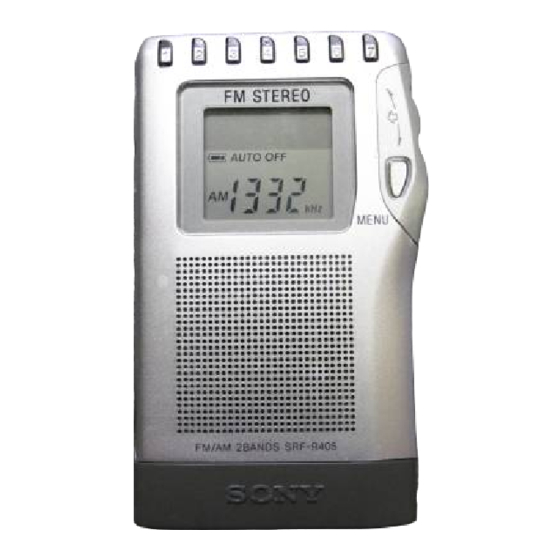
SRF-R405
SPECIFICATIONS
Frequency range
Band
Frequency range
FM
76 – 108 MHz
AM
530 – 1,710 kHz
inches) dia., 7.2 Ω
Speaker
Approx.2.8 cm (1
1
/
8
2 (headphone) jack
Output
(∅3.5 mm, stereominijack)
Power output
80 mW (at 10% harmonic distortion)
Power requirements
3 V, DC two R03 (size AAA) batteries
Power Auto Off function
Approx.30 minutes, 60 minutes,
90 minutes,120 minutes, and off
Dimensions Approx. 55 × 98 × 17 mm(w/h/d)
× 3
×
1
7
11
(2
/
/
/
inches) not incl.
4
8
16
projecting parts and controls
Approx. 59.2 × 98.2 × 17.8 mm(w/h/d)
× 3
×
3
7
23
(2
/
/
/
inches) incl.
8
8
32
projecting parts and controls
Mass
Approx. 89 g (3.1 oz) incl. batteries
Accessories Batteries (2)
Carrying case (1)
Design and specifications are subject to change
without notice.
FM STEREO/AM PLL SYNTHESIZED RADIO
Channel step
0.1 MHz
9 kHz/10 kHz
Tourist Model
Advertisement
Table of Contents

Related Manuals for Sony SRF-R405


Summary of Contents for Sony SRF-R405
- Page 1 SRF-R405 SERVICE MANUAL Tourist Model Ver 1.0 1999. 04 SPECIFICATIONS Frequency range Band Frequency range Channel step 76 – 108 MHz 0.1 MHz 530 – 1,710 kHz 9 kHz/10 kHz inches) dia., 7.2 Ω Speaker Approx.2.8 cm (1 2 (headphone) jack Output (∅3.5 mm, stereominijack)
-
Page 2: Section 1 General
SECTION 1 GENERAL Notes on chip component replacement This section is extracted • Never reuse a disconnected chip component. from instruction manual. • Notice that the minus side of a tantalum capacitor may be damaged by heat. — 2 —... -
Page 3: Section 2 Disassembly
SECTION 2 DISASSEMBLY Note : Follow the disassembly procedure in the numerical order given. 2-1. CABINET (REAR) ASSY Note : On installation of cabinet (rear), adjust the knob (earphone/speaker) and switch positions until they agree. 4 Screw (M1.7 × 5) 5 Screw (M1.4 ×... -
Page 4: Section 3 Electrical Adjustments
SECTION 3 ELECTRICAL ADJUSTMENTS 0 dB = 1 µV FM TRACKING ADJUSTMENT TUNER SECTION Adjust for a maximum reading on level meter. [FM] Setting L202 76.0MHz ENT/BAND switch : FM CT202 108.0MHz Signal generator AM VCO ADJUSTMENT FM RF signal generator Adjust so that the voltage at TP3(LPF) becomes 2.60 ±0.05V. - Page 5 SECTION 4 DIAGRAMS 4-1. BLOCK DIAGRAM B+ (+1.2V) D201-2 D201-3 L205 FM/AM FRONT END AM VCO IC201 AM OSC (+3V) L201 HP101 B+ (+1.2V) (EAR-RECEIVER) AM FERRIT-ROD ANTENNA DISCRI AM RF IN S401 D201-1 DISCRIMINATOR AM FE CT201 EAR-RECEIVER CF203 /SPEAKER R-CH FM DECODER...
-
Page 6: Printed Wiring Board
SRF-R405 4-2. PRINTED WIRING BOARD MAIN BOARD (SIDE A) MAIN BOARD (SIDE B) TP17 TP16 S506 POWER S504 S505 S503 S510 S511 S512 S502 TP11 RV401 TP12 LCD101 S501 TP10 HOLD R509 50 49 S509 R508 ENT/BAND R514 (JOG LEVER) - Page 7 4-3. SCHEMATIC DIAGRAMS • Refer to page 13 for IC Block Diagrams. SRF-R405 PLL LOW-PASS FILTER (76k) Note on Schematic Diagram: • All capacitors are in µF unless otherwise noted. pF: µµF 50 WV or less are not indicated except for electrolytics and tantalums.
- Page 8 4-4. IC PIN FUNCTION IC401 CXA1522N • IC506 µPD17073GB-921-9EU (System Control, LCD Drive) Pin No. Pin Name Description Pin No. Pin Name Description DATA OUT Serial data output terminal (Not used: open) LCD10 Segment signal output to LCD EEPROM CS Chip selection output to EEPROM (Not used: open) LCD11 Segment signal output to LCD...
-
Page 9: Section 5 Exploded Views
SECTION 5 EXPLODED VIEWS NOTE: • -XX, -X mean standardized parts, so they may • The mechanical parts with no reference number have some differences from the original one. in the exploded views are not supplied. • Items marked “*” are not stocked since they •... -
Page 10: Section 6 Electrical Parts List
SECTION 6 MAIN ELECTRICAL PARTS LIST NOTE: • Due to standardization, replacements in the • CAPACITORS: • SEMICONDUCTORS parts list may be different from the parts uF: µF In each case, u: µ, for example: specified in the diagrams or the components •... - Page 11 MAIN Ref. No. Part No. Description Remarks Ref. No. Part No. Description Remarks < DIODE > < RESISTOR > D201 8-719-023-99 DIODE KV1563M-3 R201 1-218-965-11 RES,CHIP 1/16W D202 8-713-102-96 DIODE 1T403-M20-T8A R202 1-218-989-11 RES,CHIP 1/16W D203 8-713-102-96 DIODE 1T403-M20-T8A R203 1-218-977-11 RES,CHIP 100K 1/16W...
-
Page 12: Accessories And Packing Materials
SRF-R405 MAIN Ref. No. Part No. Description Remarks Ref. No. Part No. Description Remarks R531 1-218-965-11 RES,CHIP 1/16W R532 1-218-961-11 RES,CHIP 4.7K 1/16W R544 1-218-977-11 RES,CHIP 100K 1/16W R545 1-218-989-11 RES,CHIP 1/16W R546 1-218-929-11 RES,CHIP 1/16W R548 1-218-929-11 RES,CHIP 1/16W...