
Related Manuals for Panasonic PT-47WXD63G


Summary of Contents for Panasonic PT-47WXD63G
- Page 1 Order No. MTNC031147C1 HDTV MONITOR PT-47WXD63G / PT-53WXD63G 1. Safety precautions...
- Page 2 General guidelines An isolation transformer should always be used during the servicing of a receiver whose chassis is not isolated from AC power line. Use a transformer of adequate power rating as this protects the technician from accidents resulting in personal injuryfrom electrical shocks. It will also protect the receiver from being damaged by accidental shorting that may occur during servicing.
-
Page 3: About Lead Free Solder (Pbf)
Repeat the procedure and measure the voltage present with all other exposed metallic parts. Verify that any potential does not exceed 0.75 volt RMS. A leakage current tester (such a Simpson model 229, Sencore model PR57 or equivalent) may be used in the above procedure, in which case any current measure must not exceed 0.5 milliampere.If any measurement is out of the specified limits, there is a possibility of a shock hazard and the receiver must be repaired and rechecked before it is returned to the customer. - Page 4 This model uses Pb Free solder in it’s manufacture due to environmental conservation issues. For / service and repair work, we’d suggest the use of Pb free solder as well, although Pb solder may be / used. / PCBs manufacturedusing lead free solder will have the “PbF” or a leaf symbol stamped on the / back of PCB.
-
Page 5: Important Safety Tests
3. Important safety tests Measuring H.V. The anode caps are cemented to the CRTs. To gain access for high voltage measurement, remove the red CRT’s anode lead from the flyback transformer distributor. Grasp the anode lead protective cap at its bottom and squeeze it against thelocking cap body inside, rotate 1/4 turn counter clockwise and pull the anode lead sleeve out of the FBT distributor. - Page 6 pin 1 on D-Board H.V. measurement 4. Connect a H.V. meter (static type, class 0.1) with high voltage leads to high voltage distributor on FBT. DVM and power supply connection 5. Connect the 15 ~ 25 V DC variable power supply positive lead to D34 or IC802 pin 2 (D Board) and negative lead to heat sink of Q551 or D825 Procedures:...
-
Page 7: Service Notes
4. Service notes NOTE These components are affixed with glue. Be careful not to break or damage any foil under the component or at the pins of the ICs when removing. Usually applying heat to the component for a short time while twisting with tweezers will break the component loose. Leadless chip component (surface mount) Chip components must be replaced with identical chips due to critical foil track spacing. - Page 8 a 30 watt iron until solder flows. Do not apply heat for more than 3 seconds. How to replace flat ic (required tools) 1. Remove the solder from all of the pins of a Flat IC by using a desolder braid 2.
- Page 9 4. Position the new Flat IC in place (apply the pins of the Flat IC to the soldering pads where the pins need to be soldered). Properly determine the positions of the soldering pads and pins by correctly aligning the polarity symbol 5.
-
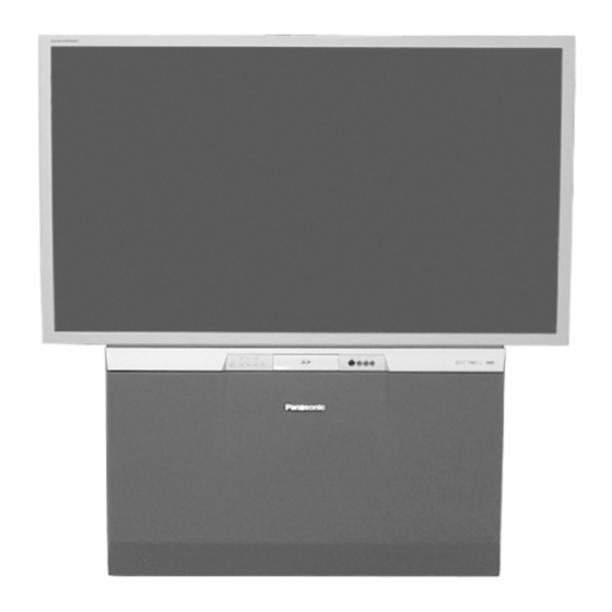
Page 10: Ptv Location Of Controls
WARNING This receiver has been designed to meet or exceed applicable safety and x-ray radiation protection as specified by government agencies and independent testing laboratories. To maintain original product safety design standards relative to x-ray radiation and shock and fire hazard, parts indicated with the symbol on the schematic must be replaced with identical parts. -
Page 11: Receiver Feature Table
6. Receiver feature table... - Page 12 FEATURE/MODEL PT-47WXD63GPT-53WXD63G CHASSIS AP830 MICRO 256K MENU LANGUAGE ENGLISH CLOSED CAPTION V-CHIP (USA/CANADA) CHANNEL INFO BANNER ATSC / QAM TUNING VIDEO INPUT SKIP SKIP CHANNEL COUNT PIP (1T), 2T PIP (2T), 2T SPLIT 2T SPLIT REMOTE CONTROL (W/LIGHT) EUR7627Z10 CRT SUPPLIER MDDA (CENTAUR) SCREEN W/PROT SCREEN...
-
Page 13: Board Description Table
Note: Specifications are subject to change without notice or obligation. 7. Board description table BOARD PART NUMBER DESCRIPTION A-BOARD TNP2AH051 MAIN CHASSIS D-BOARD TNP2AH056 POWER SUPPLY * DC-BOARD TNP2AA151 CONVERGENCE CIRCUIT * DG-BOARD TNP2AA132 MPU, VIDEO SIGNAL PROCESSING * DV-BOARD TNP2AA133 HDMI DECODER * DT-BOARD... -
Page 14: Auto Diagnosis Feature
Note: For additional information for this remote please refer to the owner’s manual section remote operation, listed on the parts list section. 9. Auto diagnosis feature This receiver incorporates a self diagnosis feature. With this feature it will be easier for the technician to detect failures. -
Page 15: Eeprom Copy Jig
This PTV has a feature that allows to clone convergence from main EEPROM data adjustments from a PTV to other by connecting a jig to the PTV set, or can be used to back-up data before making adjustments. A jig part number TXFJIG01SER, is availablethrough Matsushita/Panasonic Services. - Page 16 1. Enter to service mode and display service menu 2. Select “FINE” DAC and press OK on remote. 3. Press “8” on remote. 4. Select from and then press OK on remote: - INT to copy data from internal EEPROM to jig - EXT to copy from jig to internal EEPROM.
- Page 17 11. A-Board check points A-Board check points...
-
Page 18: Chassis & Boards Layout (Location Of Main Components)
12. Chassis & boards layout (location of main components) Chassis and boards layout... - Page 19 Chassis and boards (FRONT)
- Page 20 A-BOARD...
- Page 21 D-BOARD...
- Page 22 R-BOARD DC-BOARD (TOP)
- Page 23 DC-BOARD (BOTTOM) DV-BOARD...
- Page 24 JG-BOARD...
- Page 25 T-BOARD...
- Page 26 DG-BOARD (TOP) DG-BOARD (BOTTOM)
-
Page 27: Disassembly For Service
DT-BOARD 13. Disassembly for service NOTE: Board ground wires may have to be disconnected to disassemble some boards. All ground wires must be reconnected using jumper leads, if necessary, before power is applied to PTV for... - Page 28 service. Speaker grille removal Speaker grille, is secured to the cabinet of the PTV with 5 grommet holders. Grip panel from the sides and middle upper part, and gently pull forward to remove. When reassembling, make certain to firmly press on the panel where the insertion points(5) are located, one at each corner and one at the middle top edge.
- Page 29 Back lower cover removal 1. Remove (7) hex screws around the perimeter, marked with arrows. See figure for screws location. 2. Remove (9) screws from around the A/V terminal board (marked with arrows). Back lower cabinet removal Back cabinet removal 1.
- Page 30 Screen frame removal 1. Remove the speaker grille. Disconnect the cables leading to the keyboard, JPEG viewer and the A/V panels and remove the keyboard and AV panel assembly. The assembly is secured by three (3) screws. 2. At this point the front cover is held only by four screws, be careful not to push the cabinet forward.
- Page 31 4. Remove the horizontal barrier panel at the back of the cabinet. 5. Unplug cables connectors (K1, JG3, G1 and speaker connectors) and pull out the main chassis block. Note: Main chassis block can be serviced either in normal position or laying on its back (protect hookup terminal from damage).
- Page 32 13.1. Chassis assembly The chassis assembly shown in figure includes all the electrical and optical (light box) components Chassis back view A/V BACK COVER ASSEMBLY This assembly is secured to H-Board by 8 screws. Be sure to disconnect the fan cable from H- board.
- Page 33 1. This board has a metal frame holder that is fastened to A-Board with 2 screws. This metal frame must be removed first before trying pulling up DT-board, otherwise it can be damaged. 2. This board has grommet squares, be careful to do not screw too tight, otherwise the grommet screw hole will get stripped.
- Page 34 DG-Board 1. Plugs onto A-Board at A31 and A32 connectors (DG1 and DG2 respectively). 2. Remove plug cables from connectors DG4, DG5, DG6 and DG7. NOTE: This board is non-serviceable. / When removing this board pull carefully. A-Board 1. A-Board is secured to the chassis tray with six screws. 2.
- Page 35 D-Board 1. D-Board is secured to the chassis tray with five screws. 2. The D-Board is mated to the A-Board by four connectors (female side of connectors): D1, D2, D3 & D4. To remove this board, unplug the connectors on the A-Board pulling from the sides of each connector.
- Page 36 LR, LG and LB Board 1. Each board is plugged into the socket on the PRT neck, LR-Board on red PRT, LG-Board on green PRT and LB-Board on blue PRT. 13.2. Disassembly for CRT replacement To facilitate CRT replacement, the complete CRT mounting chassis does not need to be removed.
- Page 37 Focus pack location 8. Release CRT anode lead from CRT chassis wire clamp and all other wires from holders. 9. Loosen a screw that secures the DY and remove it from the CRT neck. Caution: To insure protection against x-ray radiation, the lens must be mounted in place at all times when power is applied to the PTV CRT replacement 1.
- Page 38 2. Lay CRT face down on a soft cloth. 3. Note position of yoke with centering tabs and remove from defective CRT. 4. Remove CRT DAG ground from defective CRT. Mount it on the replacement CRT exactly as it was on the defective CRT. Note: Replacement CRT is supplied with H.V.
-
Page 39: B + Voltages Table
13.3. PTV screen assemblies Screen assemblies 13.4. Screen assemblies warning When storing or disposing of screen assemblies, be sure not to place them in direct sunlight. These screens may act as a magnifying glass and could cause a fire. 14. B + voltages table Preparation:... -
Page 40: Service Mode (Electronic Controls)
Set the following controls - Picture to Normal - Bright to Normal - Volume to MIN (0) Procedure: 1. Apply a NTSC COLOR BAR pattern 2. Connect the negative lead of the digital voltmeter to TPGND1 (cold ground). 3. Connect the positive lead of the digital voltmeter to each test point and confirm the B+ voltages. - Page 41 2. Select TIMER icon and set SLEEP time for 30 Min. 3. Press “OK” then VOL up to exit menus. 4. Tune to the Channel 124. 5. Adjust VOLUME to minimum (0). 6. Press VOL (decrease) on receiver. Red “CHK” appears in upper corner.
- Page 42 IMPORTANT NOTE Always check that PTV exits the service mode To check colors: Press RECALL on the remote control when in service mode (red “CHK” is displayed) to enter the purity field check mode. Color check 15.3. Service adjustment default values for items DESCRIPTION REGISTER FORMAT...
- Page 43 DESCRIPTION REGISTER FORMAT NTSC (480i) 480i ZOOM 480P 480P ZOOM 1080i VERTICAL S CORRECTION VERTICAL EHT PRESET V-EHT FLYBACK EHT PRESET EHTFB MUTE CONVERGENCE MUTE COARSE ADJ COARS FINE ADJ FINE H DAF ADJUSTMENT H-PAR V SAW DAF ADJUSTMENT V-SAW V DAF ADJUSTMENT V-PAR ACL ADJUSTMENT...
- Page 44 15.5. Instructional flow for service mode (continued...)
- Page 45 16. CRT Set Up CAUTION: Insure that yoke plugs are reconnected on D-Board before turning the PTV ON to prevent damage to the horizontal output transistor and /or CRTs. 1. Connect test generator to the antenna terminal and set for a monoscope pattern.
- Page 46 VOL (RIGHT/LEFT); pressOK, to save press OK again or OTHER key to exit without saving. Procedure: NOTE: 1080i, 480p, 480i pattern can be obtained from Panasonic’s TU-DST51 set top box DTV decoder. 1. Enter to service mode and set the following default DATA H-PAR +247...
- Page 47 (use for minor adjustment or for final adjustment, for complete adjustment see following section.) Electrical Adjustment NOTE: 1080i, 480p, 480i pattern can be obtained from Panasonic’s TU-DST51 set-top box DTV decoder. 1. Apply a crosshatch with dots pattern Lens focus adjustment...
- Page 48 GREEN BLUE Electric focus Optical Focus 2. Set VIDEO “C_OFF” DAC from 00 to 02, and project only red. Adjust red focus VR so that focus is best Focus pack 3. Adjust red lens focus (mechanical) until focus is best. 4.
-
Page 49: Electronic Adjustments
This adjustment is intended to correct the horizontal position of the picture NOTE: 1080i, 480p, 480i pattern can be obtained from Panasonic’s TU-DST51 set-top box DTV decoder. 1. Apply a pattern that lets adjust the image to correct vertical size (see above note). - Page 50 7. Set VIDEO “C_OFF” DAC from 01 to 00 17.2. Centering magnets adjustment NOTE: 1080i, 480p, 480i pattern can be obtained from Panasonic’s TU-DST51 set-top box DTV decoder. Procedures: 1. Apply a crosshatch pattern with dots. 2. Set VIDEO “C_OFF” DAC from 00 to 01 to project only green.
- Page 51 This adjustment is intended to make the picture vertically proportional (top, center and bottom) NOTE: 1080i, 480p, 480i pattern can be obtained from Panasonic’s TU-DST51 set-top box DTV decoder. 1. Apply a pattern that lets adjust the image to correct vertical linearity (see above note).
- Page 52 This adjustment is intended to correct the vertical size of the picture. NOTE: 1080i, 480p, 480i pattern can be obtained from Panasonic’s TU-DST51 set-top box DTV decoder. 1. Apply a pattern that lets adjust the image to correct vertical size (see above note).
- Page 53 This adjustment is intended to correct curved sides of the picture. NOTE: 1080i, 480p, 480i pattern can be obtained from Panasonic’s TU-DST51 set-top box DTV decoder. Procedure: 1. Apply a pattern that lets adjust the image to correct curved sides (see above note) 2.
- Page 54 8. Set VIDEO “C_OFF” DAC from 01 to 00. 17.7. Trapezoid adjustment (TRAP) NOTE: 1080i, 480p, 480i pattern can be obtained from Panasonic’s TU-DST51 set-top box DTV decoder. Procedure: 1. Apply a crosshatch pattern. 2. Enter service mode, select “TRAP” and adjust DATA with VOLUME keys in remote so that lines at right and left are vertical like a solid line.
- Page 55 1080i, 480p, 480i pattern can be obtained from Panasonic’s TU-DST51 set-top box DTV decoder. 1. Apply a pattern that lets adjust the horizontal size. 2. Set VIDEO “C_OFF” DAC from 00 to 01 to project only green. 3. Set DAC “MUTE” from 00 to 01 (disabling digital convergence).
- Page 56 17.12. White balance adjustment NOTE: 1080i, 480p, 480I pattern can be obtained from Panasonic’s TU-DST51 set-top box DTV decoder. Prior to this adjustment, perform sub-contrast adjustment. This adjustment requires the service user skills in observing what a screen without color should look like (white picture).
- Page 57 17.13. Color adjustment (TINT, B-Y_G, R-Y_A) NOTE: 1080i, 480p, 480i pattern can be obtained from Panasonic’s TU-DST51 set-top box DTV decoder. This adjustment requires that the servicer use the skills in observing what a colorbar pattern should looks like.
- Page 58 look bluish. 4. Adjust “B-Y_G” so blue look natural, and the rest of the colors become in balance. 5. Adjust “R-Y_A” so red look natural, and rest of the colors become in balance. 6. Check that white bar is real white, no bluish or reddish or tending to become grey.
- Page 59 Procedure: 1. Turn the PTV “ON” with the A.C. power applied. 2. Measure TP0PLL (A-Board Connector A31 pin 56) for frequency and record the reading. Note: Pin measurement must have at least four digits of resolution following the decimal point. Example: 000.0000 3.
- Page 60 the receiver along with the release date. 5. Insert the SD service card in the back of the receiver in the slot with a sign “SERVICE ONLY”. 6. The receiver will automatically display a screen, showing the current software version of the receiver (right) and the software version stored in the SD service card (left), (i.e.
- Page 61 “JPEG Program Download” menu. NOTE: To abort the download process just press “EXIT” on remote in the “JPEG Program Download” menu. IMPORTANT: For better results in this procedure, be sure that the set is already powered ON and if the set is powered OFF, wait at least 10 seconds after turning ON the receiver before inserting the SD service card to the JPEG viewer slot.
- Page 62 software version. 3. To select one of the options press the CH keys on remote. 4. Option No. 1 will perform an auto test from option No. 2 trough No. - SDRAM Test: will perform a test of the internal memory of the JPEG reader device, showing for a few seconds a green screen followed by a magenta screen.
-
Page 63: Convergence Adjustment
Also EEPROM copy jig can be used to back-up the data before to performadjustments. NOTE: 1080i, 480p, 480i pattern can be obtained from Panasonic’s TU-DST51 set-top box DTV decoder. IMPORTANT NOTICE: It is strongly recommended to first read and understand the following section prior to make any adjustment. - Page 64 Procedure: Apply the convergence alignment template to the PTV screen frame to converge the green raster only. Remove the convergence alignment template following this alignment. The red and blue rasters can then be aligned to the green raster. Raster Set-Up: 1.
- Page 65 12. Press “TV/VIDEO” key on remote to enter “OSD_POS” mode. 13. Press “5” key on remote so that monoscope pattern appears (superimpose mode) 14. Move cursor by pressing VOL right - left and CH up - down so that cursor center overlap monoscope pattern center 15.
- Page 66 When “7” is pressed and the data is saved, it will overwrite the factory default. 18.1. Coarse adjustment mode (COARS) NOTE: 1080i, 480p, 480i pattern can be obtained from Panasonic’s TU-DST51 set-top box DTV decoder. NOTE: It is strongly recommended to first read and understand the following section prior to make any adjustment.
- Page 67 - TV/VIDEO (repeatedly) - R-TUNE (repeatedly) 2. Press “2” repeatedly and apply the pattern of border and cross. 3. Press “RECALL” key to display values 4. Adjust size so that the line of the border closes to the screen frame at top, bottom, left and right, by pressing CH up-down and VOL right -left “SIZE”...
- Page 68 12. Press “7” then “OK” key on remote to save changes “PIN” mode adjustment 13. Press “7” then “OK” key on remote to save changes 14. Adjust by pressing VOL right-left (see figure) 15. Press “7” then “OK” key on remote to save changes “CORNER”...
- Page 69 enough, repeat adjustments. 19. Enter to “STATIC” mode by pressing TV/VIDEO. 20. Press “1” or “3” repeatedly until green and red only are shown. 21. Adjust “R-STATIC” so that the center of red overlaps with the center of green “STATIC” mode adjustment 22.
- Page 70 28. Adjust so that the line on the border closes to the screen frame at top, bottom, left and right (see figure). 29. Enter to PIN “R-PIN” mode by pressing TV/VIDEO 30. Adjust horizontally and vertically (see figure) 31. Enter to CORNER “R-CORNER” mode by pressing TV/VIDEO. 32.
- Page 71 NOTE: It is strongly recommended to first read and understand the following section prior to make any adjustment. HELPFUL HINT: The easiest way to adjust convergence is to start adjusting from the center of the screen to the borders in all the convergence adjustments. Once in “FINE”...
- Page 72 PRESS BUTTON 1(go) or 3(back) change color view change pattern 4 (only FINE change crossed sections mode) overlap save data copy from clear POWER exit RECALL display values R-TUNE cycle colors TV/VIDEO change mode TV/VIDEO (3 switch convergence mode (FINE/ secs) COARSE) When “7”...
- Page 73 - Press TV/VIDEO (repeatedly) to select mode. - Press R-TUNE (repeatedly) to select color 2. Press “2” repeatedly and apply the pattern of crosshatch. 3. Press “4” frequently to change crossed sections, this helps to check convergence more accurate in more sections of the picture. 4.
- Page 74 11. To move the cursor press MUTE on the remote (cursor flashes), then move the cursor to any of the positions for “EASY” mode 12. This adjustment may help to make rounded lines become straight lines. 13. Adjust to make lines as straight as possible 14.
- Page 75 20. When slightly adjustment is needed, use “ORIG. POINT” mode. 21. To enter to “G-ORIG. POINT” (for green) mode press TV/VIDEO. 22. With “ORIG. POINT”, the adjustment data changes by 1 step, this allows more detail in the adjustment. Display values on screen by pressing RECALL on remote 23.
- Page 76 29. Perform adjustments for red so that red overlaps green, do not move green. 30. Press “1 or 3” on the remote until yellow (red and green) and blue appears, do not move green or red. 31. Perform adjustments so that blue overlaps Yellow (red and green). 32.
- Page 77 - 53” Models: 1036mm horizontal x 584mm vertical. Grid dimensions: SCREEN MODE HORIZONTAL VERTICAL 47’’ 1080i 40.00 mm 20.80 mm 53’’ 1080i 46.60 mm 23.10 mm NOTE: A convergence alignment template, part number TXFQD01ESER2 for 47” and TXFQD01FSER1 for 53” is available through Matsushita/Panasonic Services...
-
Page 78: Reference Of Pdf Links Color
19. Reference of PDF links color 20. Conductor views 20.1. A-Board Printed Circuit ( page 1 of 2 ) 20.2. A-Board Printed Circuit ( page 2 of 2 ) 20.3. D-Board Printed Circuit ( page 1 of 2) -
Page 79: Block Diagrams
20.4. D-Board Printed Circuit ( page 2 of 2) 20.5. DC-Board Printed Circuit ( bottom view) 20.6. DC-Board Printed Circuit ( top view ) 20.7. DG-Board Printed Circuit (bottom view) 20.8. DG-Board Printed Circuit ( top view ) 20.9. DT-Board Printed Circuit ( bottom view ) 20.10. - Page 81 22.2. Notas de los diagramas esquem á ticos...
- Page 83 22.3. A-Board schematic 1 of 4 22.4. A-Board schematic 2 of 4 22.5. A-Board schematic 3 of 4 22.6. A-Board schematic 4 of 4 22.7. D-Board schematic 1 of 6 22.8. D-Board schematic 2 of 6 22.9. D-Board schematic 3 of 6 22.10.
- Page 84 22.27. DT-Board schematic 6 of 15 22.28. DT-Board schematic 7 of 15 22.29. DT-Board schematic 8 of 15 22.30. DT-Board schematic 9 of 15 22.31. DT-Board schematic 10 of 15 22.32. DT-Board schematic 11 of 15 22.33. DT-Board schematic 12 of 15 22.34.
-
Page 85: Parts Location
22.53. LG-Board schematic 2 of 2 22.54. LR-Board schematic 1 of 2 22.55. LR-Board schematic 2 of 2 22.56. T-Board schematic 1 of 2 22.57. T-Board schematic 2 of 2 22.58. Voltages 22.59. Waveforms 23. Parts location 24. Parts list 24.1. - Page 86 24.2. Parts list Ref. No. Part No. Part Name & Description Remarks CAPACITORS C001 ECEA1CKA470B CAP E 47UF-16V C002 ECJ2VC1H220J CAP C 22PF-J-50V C003 ECJ2VC1H220J CAP C 22PF-J-50V C004 ECEA1HKA4R7B CAP E 4.7UF-50V C005 ECEA1HKA2R2B CAP E 2.2UF-50V C006 EEUFC1A471B CAP E 470UF-10V C011 ECJ2VF1H104Z...
- Page 87 Ref. No. Part No. Part Name & Description Remarks C312 ECKC3D102KBN CAP C 1000PF -K-2KV C313 ECKR2H102KB5 CAP C 1000PF -K-500V C331 F2A1H470A162 CAP E 47UF-50V C332 ECKR1H103ZF5 CAP C .01UF-Z-50V C333 F2A1H470A162 CAP E 47UF-50V C334 F2A2E470A026 CAP E 47UF-250V C335 ECCR1H221JC5 CAP C 220PF-J-50V...
- Page 88 C525 ECEA1HN220UB CAP E 22UF-50V...
- Page 89 Ref. No. Part No. Part Name & Description Remarks C526 ECA2EM101E CAP E 100UF-250V C527 ECKR2H102KB5 CAP C 1000PF -K-500V C528 ECA1HM470B CAP E 47UF-50V C531 ECA160V33UE CAP E 33UF-160V C533 ECKR2H101KB5 CAP C 100UF-K-500V C535 ECA1EM471E CAP E 470UF-25V C601 EEUFC1C331B CAP E 330UF-16V...
- Page 90 Ref. No. Part No. Part Name & Description Remarks C849 ECKR1H223ZF5 CAP C .022UF-Z-50V C851 ECQV1H104JL3 CAP P .10UF-J-50V C852 ECA1EM101B CAP E 100UF-25V C854 ECA1CM101B CAP E 100UF-16V C855 ECJ2VF1H104Z CAP C .1UF-Z-50V C860 EEUFC1V561E CAP E 560UF-35V C861 ECJ3VF1H224Z CAP C .22UF-Z-50V C863...
- Page 91 Ref. No. Part No. Part Name & Description Remarks C945 F2A1C101A159 CAP E 100UF-16V C947 F2A2C100A023 CAP E 10UF-160V C962 ECKR1H103ZF5 CAP C .01UF-Z-50V C963 ECQM2103KZB CAP P .01UF-K-200V C965 ECKR1H103ZF5 CAP C .01UF-Z-50V C966 ECQM2103KZB CAP P .01UF-K-200V C967 F2A2C100A023 CAP E 10UF-160V C968...
- Page 92 Ref. No. Part No. Part Name & Description Remarks C2338 ECA50YT2R2KB CAP E 2.2UF-50V C2342 ECJ2VB1H333K CAP C .033UF-K-50V C2344 ECQB1H224JF3 CAP P .22UF-J-50V C2345 EEUFC1E222E CAP E 2200UF-25V C2346 ECJ2VB1H561K CAP C 560PF-K-50V C2347 ECJ3VB1H104K CAP C .1UF-K-50V C2351 F1J1C225A083 CAP C 2.2UF-Z-16V C2352...
- Page 93 Ref. No. Part No. Part Name & Description Remarks C2588 ECA1CM102B CAP E 1000UF-16V C2589 ECJ2VF1H104Z CAP C .1UF-Z-50V C2599 ECJ2VB1C104K CAP C .1UF-K-16V C2803 ECCR1H470J5 CAP DISC 47-5-50V C2804 ECCR1H102J5 CAP C 1000PF -50V C2805 ECKW3D471KBP CAP C 470PF-K-2KVDC C2806 ECES2DG101DG CAP E 100UF-200V...
- Page 94 Ref. No. Part No. Part Name & Description Remarks DIODES D002 MAZ31500ML DIODE ZENER D003 MAZ41500MF DIODE ZENER D004 MAZ31500ML DIODE ZENER D005 MAZ41500MF DIODE ZENER D081 LN21RCPHL DIODE D082 MAZ40560MF DIODE ZENER D083 MAZ40560MF DIODE ZENER D301 MA2C16700E DIODE D302 MAZ41000LF DIODE ZENER...
- Page 95 D513 MA2C165001VT DIODE Ref. No. Part No. Part Name & Description Remarks D515 D1NL40V70 DIODE D516 EU2YXV0 DIODE D519 AU02ZV0 DIODE D520 MA3X152K0L DIODE D634 MA2C165001VT DIODE D650 MAZ41100MF DIODE ZENER D651 MAZ41100MF DIODE ZENER D656 MAZ41100MF DIODE ZENER D657 MAZ41100MF DIODE ZENER D659...
- Page 96 Ref. No. Part No. Part Name & Description Remarks D1510 MAZ30330LL DIODE ZENER D1599 MA3X152K0L DIODE D2321 MA3X152K0L DIODE D2323 MA3X152K0L DIODE D2324 MA3X152K0L DIODE D2802 B0EBKT000003 DIODE D2806 MAZ41100MF DIODE ZENER D2809 MA2C165001VT DIODE D2810 EG01AF7 DIODE D2811 AG01ZV0 DIODE D2813 B0HBSM000034...
- Page 97 IC874 C0DAAZH00009 5V REGULATOR...
- Page 98 Ref. No. Part No. Part Name & Description Remarks IC880 AN78N12-LB 12V REGULATOR IC1101 TVR2AJ173S MAIN EEPROM IC1112 TVR2AJ174S CONVERGENCE EEPROM IC1501 AN6562S-E1 EHT ADJ. OP-AMP IC2302 C1AA00000645 AUDIO AMPLIFIER IC2451 NJW1137MPTE1 BBE VIVA PROCESSOR IC2801 C0DACZH00003 20V REGULATOR (HOT) IC2803 AN1431T-TA IC2804...
- Page 99 Ref. No. Part No. Part Name & Description Remarks L821 EXCELDR35V FERRITE BEAD L825 TALL08T330KA COIL L826 TALL08T330KA COIL L827 TALL08T330KA COIL L851 TALL08T470KA COIL L852 G0ZZ00001909 INT CKT L853 TALL08T220KA COIL L854 EXCELDR35V FERRITE BEAD L876 G0ZZ00001909 INT CKT L879 G0ZZ00001909 INT CKT...
- Page 100 Ref. No. Part No. Part Name & Description Remarks Q331 2SC3526H TRANSISTOR Q353 2SC3942LB TRANSISTOR Q354 B1BAAN000025 TRANSISTOR Q355 B1BCAN000004 TRANSISTOR Q361 2SC3311ATA TRANSISTOR Q362 2SC3311ATA TRANSISTOR Q363 2SC3526H TRANSISTOR Q364 2SA1309ATA TRANSISTOR Q365 2SC3311ATA TRANSISTOR Q366 2SC3311ATA TRANSISTOR Q368 2SA1309ATA TRANSISTOR Q373...
- Page 101 Ref. No. Part No. Part Name & Description Remarks Q961 2SB1321ARA TRANSISTOR Q964 2SD1992ARA TRANSISTOR Q965 2SA720TA TRANSISTOR Q966 2SC1318ATA TRANSISTOR Q967 2SC1318ATA TRANSISTOR Q968 2SA720TA TRANSISTOR Q1503 2SA1309ATA TRANSISTOR Q1504 B1BAAV000003 TRANSISTOR Q1505 2SC3311ATA TRANSISTOR Q2301 2SB709ARTX TRANSISTOR Q2302 2SB709ARTX TRANSISTOR Q2304...
- Page 102 Ref. No. Part No. Part Name & Description Remarks R080 ERDS2TJ222T RES C 2.2K -J-1/4W R081 ERDS2TJ222T RES C 2.2K -J-1/4W R082 ERDS2TJ332T RES C 3.3K -J-1/4W R083 ERDS2TJ512T RES C 5.1K -J-1/4W R084 ERDS2TJ912T RES C 9.1K -J-1/4W R086 ERDS2TJ681T RES C 680-J-1/4W R087...
- Page 103 Ref. No. Part No. Part Name & Description Remarks R369 ERDS2TJ472T RES C 4.7K -J-1/4W R371 EROS2THF4700 RES M 470-f-1/4w R372 EROS2THF82R0 RES M 82.0-f-1/4w R374 ERDS1FJ103T RES C 10K-J-1/2w R375 ERDS2TJ470T RES C 47-J-1/4W R376 ERG7ZJ272 RES M 2.7K -J-7W R379 ERDS2TJ563T RES C 56K-J-1/4W...
- Page 104 Ref. No. Part No. Part Name & Description Remarks R519 ERQ12HKR22P RES F .22-K-1/2W R520 ERQ12HJ330P RES F 33-J-1/2W R521 EROS2THF2702 RES M 27k-f-1/4w R522 EROS2THF7681 RES M 7.68k-f-1/4w R523 ERDS2TJ275T RES C 2.7MEG-J-1/4W R525 ERJ6GEYJ152V RES M 1.5K -J-1/10W R534 EROS2THF1203 RES M 120K-F-1/4W...
- Page 105 Ref. No. Part No. Part Name & Description Remarks R867 ERJ6GEYJ472V RES M 4.7K -J-1/10W R888 ERJ6ENF1001V RES M 1K-F-1/10W R889 ERJ6ENF1001V RES M 1K-F-1/10W R893 ERJ6ENF1001V RES M 1K-F-1/10W R895 ERJ6GEYJ100V RES M 10-J-1/10W R896 ERJ6ENF1001V RES M 1K-F-1/10W R897 ERJ6ENF3001V RES M 3K-F-1/10W...
- Page 106 Ref. No. Part No. Part Name & Description Remarks R957 ERDS2TJ8R2T RES C 8.2-J-1/4W R958 ERG3SJS221H RES M 220-J-3W R959 ERDS2TJ471T RES C 470-J-1/4W R961 ERDS2FJ122T RES C 1.2K -J-1/2W R962 ERDS2TJ103T RES C 10K-J-1/4W R963 ERDS2TJ683T RES C 68K-J-1/4W R964 ERDS2TJ683T RES C 68K-J-1/4W...
- Page 107 Ref. No. Part No. Part Name & Description Remarks R2226 ERDS2TJ220T RES C 22-J-1/4W R2227 ERDS2TJ220T RES C 22-J-1/4W R2228 ERDS2TJ220T RES C 22-J-1/4W R2229 ERDS2TJ220T RES C 22-J-1/4W R2230 ERDS2TJ220T RES C 22-J-1/4W R2231 ERDS2TJ220T RES C 22-J-1/4W R2232 ERDS2TJ220T RES C 22-J-1/4W R2233...
- Page 108 Ref. No. Part No. Part Name & Description Remarks R2371 ERJ6GEYJ101V RES M 100-J-1/10W R2372 ERJ6GEYJ101V RES M 100-J-1/10W R2373 ERJ6GEYJ101V RES M 100-J-1/10W R2374 ERJ6GEYJ220V RES M 22-J-1/10W R2375 ERJ6GEYJ220V RES M 22-J-1/10W R2376 ERDS2TJ220T RES C 22-J-1/4W R2377 ERDS2TJ220T RES C 22-J-1/4W R2378...
- Page 109 Ref. No. Part No. Part Name & Description Remarks R2519 ERJ6GEYJ100V RES M 10-J-1/10W R2520 ERJ6GEYJ100V RES M 10-J-1/10W R2537 ERJ6GEYJ122V RES M 1.2K -J-1/10W R2538 ERJ6GEYJ122V RES M 1.2K -J-1/10W R2539 ERJ6GEYJ122V RES M 1.2K -J-1/10W R2541 ERJ6GEYJ122V RES M 1.2K -J-1/10W R2542 ERJ6GEYJ122V RES M 1.2K -J-1/10W...
- Page 110 Ref. No. Part No. Part Name & Description Remarks R3036 ERJ6GEYJ184V RES M 180K-J-1/10W R3044 ERJ6GEYJ222V RES M 2.2K -J-1/10W R3045 ERJ6GEYJ103V RES M 10K-J-1/10W R3046 ERJ6GEYJ222V RES M 2.2K -J-1/10W R3047 ERJ6GEYJ102V RES M 1K-J-1/10W R3048 ERJ6GEYJ152V RES M 1.5K -J-1/10W R3049 ERJ6GEYJ104V RES M 100K-J-1/10W...
- Page 111 MIRROR GLASS / PT-47WXD63G TKG2AA50111 MIRROR GLASS / PT-53WXD63G TMW2AX0041B MIRROR BRACKET (SIDE) TMW2AX0161 MIRROR BRACKET (TOP) TKG2AD00071 PROTECTIVE SCREEN PANEL / PT-47WXD63G TKG2AD00091 PROTECTIVE SCREEN PANEL / PT-53WXD63G TKG2AH50381 LENTICULAR SCREEN / PT-53WXD63G TKG2AH50461 LENTICULAR SCREEN / PT-47WXD63G TKG2AH50611...
- Page 112 Ref. No. Part No. Part Name & Description Remarks UDQFSEH58F TXFKP20GSER REAR BRACKET TKD2AX1857S FRONT PANEL TXFKP19GSER DOOR PANEL TXFKP18GSER CONTROL PANEL TBX2AA2801G BUTTON KEYPAD TKP2AA0921 LED PANEL TEK6935 LATCH M005 ENPE633 SPLITTER M006 TMM2AE10171 GROMMET SQUARE K1NA68B00035 PC-BOARD CONNECTOR K1NA12B00002 SD-CARD CONNECTOR JK1001...
- Page 113 A-BOARD 1 of 4 TNP2AH051 PT-47WXD63G / PT-53WXD63G...
- Page 114 JK8007 A-BOARD 2 of 4 TNP2AH051 PT-47WXD63G / PT-53WXD63G...
- Page 115 A-BOARD 3 of 4 TNP2AH051 PT-47WXD63G / PT-53WXD63G...
- Page 116 A-BOARD 4 of 4 TNP2AH051 PT-47WXD63G / PT-53WXD63G...
- Page 117 A-BOARD 1 of 2 TNP2AH051 PT-47WXD63G / PT-53WXD63G...
- Page 118 A-BOARD 2 of 2 TNP2AH051 PT-47WXD63G / PT-53WXD63G...
-
Page 119: Audio Signal Path Block Diagram
Audio signal path block diagram H-BOARD DG-BOARD IC3002 JK3002 DTV 1 L-IN C-22 C-22 L OUT1 R-IN C-20 C-20 R OUT1 DTV 2 C-26 C-26 C-24 C-24 PROG/ VAO OUT L OUT3 R OUT3 IC3001 C-16 C-16 L OUT2 C-14 C-14 R OUT2 L OUT1... - Page 120 A-BOARD IC2451 L-IN OUTa R-IN OUTb R-IN L-IN A-MUTE MUTE VAO MUTE IC2302 L-OUT R-OUT VAO MUTE CIRCUIT Right Left Speakers Speakers AUDIO MUTE MUTE PT-47WXD63G / PT-53WXD63G IC1002 JK1001...
- Page 121 D-BOARD 1 of 6 TNP2AH056 PT-47WXD63G / PT-53WXD63G...
- Page 122 D-BOARD 2 of 6 TNP2AH056 PT-47WXD63G / PT-53WXD63G...
- Page 123 D-BOARD 3 of 6 TNP2AH056 PT-47WXD63G / PT-53WXD63G...
- Page 124 D-BOARD 4 of 6 TNP2AH056 PT-47WXD63G / PT-53WXD63G...
- Page 125 D-BOARD 5 of 6 TNP2AH056 PT-47WXD63G / PT-53WXD63G...
- Page 126 D-BOARD 6 of 6 TNP2AH056 PT-47WXD63G / PT-53WXD63G...
- Page 127 D-BOARD 1 of 2 TNP2AH056 PT-47WXD63G / PT-53WXD63G...
- Page 128 D-BOARD 2 of 2 TNP2AH056 PT-47WXD63G / PT-53WXD63G...
- Page 129 DC-BOARD 1 of 1 TNP2AA151 PT-47WXD63G / PT-53WXD63G...
- Page 130 DC-PCB BOTTOM VIEW TNP2AA151 PT-47WXD63G / PT-53WXD63G...
- Page 131 DC-PCB TOP VIEW TNP2AA151 PT-47WXD63G / PT-53WXD63G...
- Page 132 DG-BOARD 1 of 8 TNP2AA132 PT-47WXD63G / PT-53WXD63G...
- Page 133 DG-BOARD 2 of 8 TNP2AA132 PT-47WXD63G / PT-53WXD63G...
- Page 134 DG-BOARD 3 of 8 TNP2AA132 PT-47WXD63G / PT-53WXD63G...
- Page 135 DG-BOARD 4 of 8 TNP2AA132 PT-47WXD63G / PT-53WXD63G...
- Page 136 DG-BOARD 5 of 8 TNP2AA132 PT-47WXD63G / PT-53WXD63G...
- Page 137 DG-BOARD 6 of 8 TNP2AA132 PT-47WXD63G / PT-53WXD63G...
- Page 138 DG-BOARD 7 of 8 TNP2AA132 PT-47WXD63G / PT-53WXD63G...
- Page 139 DG-BOARD 8 of 8 TNP2AA132 PT-47WXD63G / PT-53WXD63G...
- Page 140 DG-PCB BOTTOM VIEW TNP2AA132 PT-47WXD63G / PT-53WXD63G...
- Page 141 DG-PCB TOP VIEW TNP2AA132 PT-47WXD63G / PT-53WXD63G...
- Page 142 DT-BOARD 1 of 15 TNP2AA144 PT-47WXD63G / PT-53WXD63G...
- Page 143 DT-BOARD 2 of 15 TNP2AA144 PT-47WXD63G / PT-53WXD63G...
- Page 144 DT-BOARD 3 of 15 TNP2AA144 PT-47WXD63G / PT-53WXD63G...
- Page 145 DT-BOARD 4 of 15 TNP2AA144 PT-47WXD63G / PT-53WXD63G...
- Page 146 DT-BOARD 5 of 15 TNP2AA144 PT-47WXD63G / PT-53WXD63G...
- Page 147 DT-BOARD 6 of 15 TNP2AA144 PT-47WXD63G / PT-53WXD63G...
- Page 148 DT-BOARD 7 of 15 TNP2AA144 PT-47WXD63G / PT-53WXD63G...
- Page 149 DT-BOARD 8 of 15 TNP2AA144 PT-47WXD63G / PT-53WXD63G...
- Page 150 DT-BOARD 9 of 15 TNP2AA144 PT-47WXD63G / PT-53WXD63G...
- Page 151 DT-BOARD 10 of 15 TNP2AA144 PT-47WXD63G / PT-53WXD63G...
- Page 152 DT-BOARD 11 of 15 TNP2AA144 PT-47WXD63G / PT-53WXD63G...
- Page 153 VDT-BOARD 12 of 15 TNP2AA144 PT-47WXD63G / PT-53WXD63G...
- Page 154 DT-BOARD 13 of 15 TNP2AA144 PT-47WXD63G / PT-53WXD63G...
- Page 155 DT-BOARD 14 of 15 TNP2AA144 PT-47WXD63G / PT-53WXD63G...
- Page 156 DT-BOARD 15 of 15 TNP2AA144 PT-47WXD63G / PT-53WXD63G...
- Page 157 DT-PCB BOTTOM VIEW TNP2AA144 PT-47WXD63G / PT-53WXD63G...
- Page 158 DT-PCB TOP VIEW TNP2AA144 PT-47WXD63G / PT-53WXD63G...
- Page 159 DV-BOARD 1 of 5 TNP2AA133 PT-47WXD63G / PT-53WXD63G...
- Page 160 DV-BOARD 2 of 5 TNP2AA133 PT-47WXD63G / PT-53WXD63G...
- Page 161 DV-BOARD 3 of 5 TNP2AA133 PT-47WXD63G / PT-53WXD63G...
- Page 162 DV-BOARD 4 of 5 TNP2AA133 PT-47WXD63G / PT-53WXD63G...
- Page 163 DV-BOARD 5 of 5 TNP2AA133 PT-47WXD63G / PT-53WXD63G...
- Page 164 DV-PCB BOTTOM VIEW TNP2AA133 PT-47WXD63G / PT-53WXD63G...
- Page 165 DV-PCB TOP VIEW TNP2AA133 PT-47WXD63G / PT-53WXD63G...
- Page 166 PROGRAM H-BOARD 1 of 3 TNP2AA134 PT-47WXD63G / PT-53WXD63G...
- Page 167 H-BOARD 2 of 3 TNP2AA134 PT-47WXD63G / PT-53WXD63G...
- Page 168 H-BOARD 3 of 3 TNP2AA134 PT-47WXD63G / PT-53WXD63G...
- Page 169 H-PCB TNP2AA134 PT-47WXD63G / PT-53WXD63G...
- Page 170 JG-BOARD 1 of 4 TNP2AA140 PT-47WXD63G / PT-53WXD63G...
- Page 171 JG-BOARD 2 of 4 TNP2AA140 PT-47WXD63G / PT-53WXD63G...
- Page 172 JG-BOARD 3 of 4 TNP2AA140 PT-47WXD63G / PT-53WXD63G...
- Page 173 JG-BOARD 4 of 4 TNP2AA140 PT-47WXD63G / PT-53WXD63G...
- Page 174 JG-PCB BOTTOM VIEW TNP2AA140 PT-47WXD63G / PT-53WXD63G...
- Page 175 JG-PCB TOP VIEW TNP2AA140 PT-47WXD63G / PT-53WXD63G...
- Page 176 K-BOARD TNP2AA149 / G-BOARD TNP2AA150 / R-BOARD TNPA0615AB PT-47WXD63G / PT-53WXD63G...
- Page 177 G-BOARD / K-BOARD / R-BOARD TNP2AA150 / TNP2AA149 / TNPA0615 PT-47WXD63G / PT-53WXD63G...
- Page 178 LB-BOARD 1 of 2 TNP2AA147AB PT-47WXD63G / PT-53WXD63G...
- Page 179 LB-BOARD 2 of 2 TNP2AA147AB PT-47WXD63G / PT-53WXD63G...
- Page 180 LB-BOARD TNP2AA147 PT-47WXD63G / PT-53WXD63G...
- Page 181 LG-BOARD 1 of 2 TNP2AA146AB PT-47WXD63G / PT-53WXD63G...
- Page 182 LG-BOARD 2 of 2 TNP2AA146AB PT-47WXD63G / PT-53WXD63G...
- Page 183 LG-BOARD TNP2AA146 PT-47WXD63G / PT-53WXD63G...
- Page 184 LR-BOARD 1 of 2 TNP2AA145AB PT-47WXD63G / PT-53WXD63G...
- Page 185 LR-BOARD 2 of 2 TNP2AA145AB PT-47WXD63G / PT-53WXD63G...
- Page 186 PT-47WXD63G / PT-53WXD63G LR-BOARD TNP2AA145...
- Page 187 T-BOARD 1 of 2 TNP2AA136 PT-47WXD63G / PT-53WXD63G...
- Page 188 T-BOARD 2 of 2 TNP2AA136 PT-47WXD63G / PT-53WXD63G...
- Page 189 T-BOARD TNP2AA136 PT-47WXD63G / PT-53WXD63G...
-
Page 190: Video Signal Path Block Diagram
Video signal path block diagram A-BOARD DG-BOARD MAIN TUNER IC4011 H-BOARD JK3001 A-23 A-23 S-VIDEO A-22 A-22 C-17 C-17 IC3001 A-18 A-18 S-VIDEO A-17 A-17 C-11 C-11 PROG Main JK3002 DTV 1 IC4002 C-32 C-32 C-30 C-30 IC3002 C-28 C-28 DG4 1 DTV 2 A-31... - Page 191 A-BOARD IC4011 Q2528 Q2525 Q2522 Q932 Q2503 Q2502 Q2501 Q931 Q2506 Q2505 Q2504 Q933 Q2509 Q2508 Q2507 IC4001 LG-BOARD LR-BOARD LB-BOARD IC4501 DG4 1 G-BOARD PT-47WXD63G / PT-53WXD63G FRONT JK1001 V S-VIDEO...
- Page 192 4.10 4.00 18.60 0.70 2.80 Q2525 Q2528 Q2801 Q2802 Q2803 Q931 Q932 Q933 3.40 3.50 0.00 0.70 2.90 6.70 5.00 19.20 11.40 11.40 10.30 0.00 10.90 18.80 6.10 19.40 2.80 2.90 10.40 0.00 2.30 6.10 4.40 -0.70 MODELS (PT-47WXD63G, PT-53WXD63G)
- Page 193 ..12.00 3.80 11.60 171.60 171.60 0.70 0.00 0.40 0.40 Q938 Q941 Q951 Q952 Q953 Q955 Q956 137.90 1.00 -0.90 -1.10 -1.10 129.70 9.60 130.10 9.00 19.30 19.30 19.30 70.00 70.00 138.60 0.30 0.00 0.00 0.00 130.10 9.00 MODELS (PT-47WXD63G, PT-53WXD63G)
- Page 194 ..8.20 ..1.90 A . . . 0.00 ..0.00 ..0.00 ..15.70 ..1.90 ..-8.20 MODELS (PT-47WXD63G, PT-53WXD63G)
- Page 195 ..0.00 ..0.80 ..3.30 ..10.00 ..3.30 ..2.10 ..10.00 MODELS (PT-47WXD63G, PT-53WXD63G)
- Page 196 3.36 Vp-p 0.176 Vp-p 0.472 Vp-p A3 PIN 9 (VD TO CONV) A3 PIN 11 (HD TO CONV) A2 PIN 15 (SOS) A3 PIN 13 (H-SYNC) 3.52 Vp-p 3.6 Vp-p A3 PIN 15 (HBLK) A3 PIN 16 (EW) MODELS (PT-47WXD63G, PT-53WXD63G)
- Page 197 2.02 Vp-p D22 PIN 2 (BV) D22 PIN 3 (BH) D22 PIN 4 (GV) 1.94 Vp-p 1.17 Vp-p .824 Vp-p D22 PIN 6 (RV) D22 PIN 7 (RH) D22 PIN 5 (GH) LG-Board TNP2AA146 28.4 Vp-p TP22 (HEATER) MODELS (PT-47WXD63G, PT-53WXD63G)