
Related Manuals for Panasonic SA-PM25


Summary of Contents for Panasonic SA-PM25
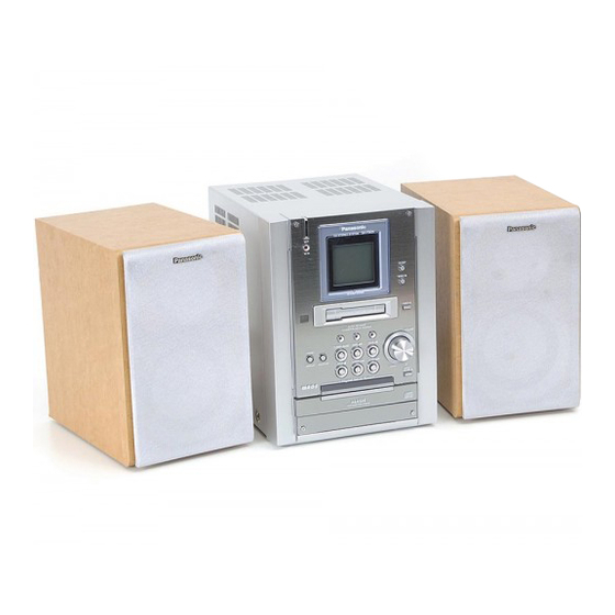
- Page 1 ORDER NO. MD0107176C3 CD Stereo System SA-PM25 Colour (S)... Silver Type Area (GD)... South Korea TAPE SECTION AR2 MECHANISM SERIES CD SECTION RAE0155Z-1V TRAVERSE DECK SERIES SPECIFICATIONS Specification...
- Page 2 Amplifier Section Power output THD 10%, both channels driven 100 Hz, both channels driven, 9 W (6 (LOW) 1 kHz, both channels driven 5 W (6 (HIGH) Total BI-AMP power 14 W PMPO power output Total BI-AMP power 160 W Input sensitivity 250 mV Input impedance...
- Page 3 1. Specifications are subject to change without notices. Mass and dimensions are approximate. 2. Total harmonic distortion is measured by the digital spectrum analyzer. Music Center: SA-PM25 (GD) System: SC-PM25 (GD) Speaker: SB-PM25 (EG) 1. Before Repair and Adjustment Disconnect AC power, discharge Power Supply Capacitors C512 through a 10 , 5W resistor to ground.
- Page 4 Note: When the protection circuitry functions, the unit will not operate unless the power is first turned off and then on again. 3. Accessories Note : Refer to Packing Materials & Accessories for part number. Remote Control Transmitter AC Power Supply FM Indoor Antenna AM Loop Antenna 4.
- Page 5 damage to the laser diode. 3. Take care not to apply excessive stress to the flexible board (FPC board). 4. Do not turn the variable resistor (laser power adjustment). It has already been adjusted. Grounding for electrostatic breakdown prevention 1. Human body grounding Use the anti-static wrist strap to discharge the static electricity from your body.
- Page 6 Caution when Replacing the Optical Pickup : The traverse has a short point shorted with solder to protect the laser diode against electrostatics breakdown. Be sure to remove the solder from the short point before making connections. 5. Precaution of Laser Diode Caution : This product utilizes a laser diode with the unit turned "ON", invisible laser radiation is emitted from the pick up lens.
- Page 7 1. Die Lasereinheit nicht zerlegen, da die Strahlung an der freigelegten Laserdiode gefährlich ist. 2. Den werkseitig justierten Einstellregler der Lasereinhit nicht verstellen. 3. Nicht mit optischen Instrumenten in die Fokussierlinse blicken. 4. Nicht über längere Zeit in die Fokussierlinse blicken. ADVARSEL : I dette a apparat anvendes laser.
- Page 8 7. Disassembly and Main Component Replacement Procedures “ATTENTION SERVICER” Some chassis components may have sharp edges. Be careful when disassembling and servicing. 1. This section describes procedures for checking the operation of the major printed circuit boards and replacing the main...
-
Page 9: Table Of Contents
components. 2. For reassembly after operation checks or replacement, reverse the respective procedures.Special reassembly procedures are described only when required. 3. Select items from the following index when checks or replacement are required. 4. Refer the Parts No. on the page of "Main Component Replacement Procedures", if necessary. - Page 10 Step 3 Release connector CS802 and PW802. Step 4 Remove 10 screws.
-
Page 11: Checking For The Main P.c.b
- Check the Transformer P.C.B. as shown. 7.1.2. Checking for the Main P.C.B. Step 5 Remove 2 screws Step 6 Push claws both side and bottom. Release connectors CS601A and CN1301 between Panel P.C.B. and Main P.C.B. Push front panel forward. - Check the Main P.C.B. -
Page 12: Checking For Thepower P.c.b And Deck P.c.b
Step 1 Lift up the CD unit and place it as shown in the following figure. - Check the CD Servo P.C.B. as shown. 7.1.4. Checking for the Power P.C.B and Deck P.C.B.. -
Page 13: Disassembly Of The Disc Tray
Step 2 Lift up the Main P.C.B. together with the Power P.C.B. and rotate left then place the P.C.B. as shown in the following figure. - Check the Power P.C.B. as shown. 7.2. Disassembly and Assembly of the Disc Tray and CD Traverse Unit 7.2.1. -
Page 14: Disassembly Of The Cd Traveerse Unit
Step 1 Turn the gear counter clock wise until the CD Tray starts to move out. Step 2 Release the 2 claws and remove the clamp plate in the direction of the arrow. Step 3 Lift up the CD Tray to remove it. 7.2.2. -
Page 15: Main Component Replacement Procedure
Step 1 Release the 2 claws and remove the CD Traverse Unit in the direction of the arrow. NOTE : 1. Follow the reverse procedure to replace the CD Traverse Unit and CD Tray. 2. Make sure that the 2 gear is in position shown above and the hole on the right gear is align with the hole below it when replacing the CD Traverse Unit and CD Tray. -
Page 16: Replacement Of The Cd Servo P.c.b. And Optical Pick-Up Unit
7.3.1. Replacement of the CD Servo P.C.B. and Optical Pick-up Unit. Step 2 Desolder the 4 legs of 2 motors and flip over the CD Servo P.C.B. Step 3 Remove the flexible cable at CN701. - Removal of the flexible cable / Push the top of the connector in the direction of the arrow 1 and then pull out the flexible cable in the direction of the arrow 2. - Page 17 Step 6 Release the claw and remove the Driver Plate. Step 7 Slide out the Optical Pick-up Unit from the indent opening.
- Page 18 NOTE : Do not touch the Lense on the OPU. 8. Self-Diagnostic Display Function This unit is equipped with a self-diagnostic function which, in the event of a malfunction, automatically display a code indication the nature of the malfunction. Use this self-diagnostic function when servicing the unit.
- Page 19 5. Load a pre-recorded tape with both side record tabs intact and close the cassette holder. 6. Press "Tape Play" (After TPS function, tape will stop automatically). 7. Press "Tape Record". 8. Press "Stop" to indicate Error code.ve). ~ If several problem exist, error code will change each time when "Stop"...
- Page 20 Error Code Problem Condition Possible Cause Cassette deck MODE SW detection error. maifunctions Faulty contact or short circuit of mechanism mode switch. (S971) Recording not possible REC INH SW detection error. Faulty contact or short circuit of REC INH switch. (S974, S975) Playback cannot HALF SW detection error.
- Page 21 4. Playback the playback gain adjustment portion(315Hz, 0dB) of test tape(QZZCFM). Check if level difference between forward and reverse direction is within 1.5dB. 5. After the adjustment, apply screwlock to the azimuth adjusting screw. Fig. 1 Fig. 2 Fig. 3 9.1.2.
- Page 22 Fig. 5 9.1.3. Bias Vlotage Check 1. Connect the measuring instrument as shown in Fig. 6. 2. Set the unit to “AUX” position. 3. Insert the normal blank tape (QZZCRA) and set the unit to “REC” mode (use “ REC/STOP” key). 4.
- Page 23 9.2. Tuner Section 9.2.1. AM-IF Alignment SIGNAL GENERATOR or SWEEP RADIO DIAL INDICATOR ADJUSTMENT REMARKS GENERATOR SETTING (ELECTRONIC (Shown in Fig. 3) VOLTMETER or CONNECTIONS FREQUENCY OSCILLOSCOPE) Fashion a loop 450kHz 30% Point of non- Headphones Z2 (AM IFT) Adjust of several turns Mod.
- Page 24 <Tuner> Fig. 9 Fig. 10 10. Illustration of IC’s, Transistors and Diodes...
- Page 25 11. Terminal Function of IC's 11.1. IC1 (LA1833NMNTLM) : IF & MPX IC (TUNER) Mark Function FM IF In — D signal det. capacitor connection terminal AM MIX Laser amp output terminal Photo diode light quantity det. input terminal AM IF In Laser amp reverse input terminal APC amp criterion voltage...
- Page 26 Mark Function Off track detection signal output terminal OSC OUT — GND terminal 11.2. IC2 (LC72131MDTRM) : PLL IC (TUNER) Mark Function — 3.3V external transistor control terminal (Not used, open) — 3.3V regular output monitor terminal (Not used, connected to GND) —...
- Page 27 11.3. IC701 (AN8885SBE1) Servo Amplifier Pin No. Mark Function Tracking signal input 1 Tracking signal input 2 Power supply Focus signal input terminal 1 Focus signal input terminal 2 APC amp input APC amp output RFsumming output RFIN Detector’s input CSBRT I Capacitor for OFTR connection...
- Page 28 Pin No. Mark I/O Function BCLK Bit Clock Output for Serial Data LRCK L/P Clock Signal Output SRDATA Serial Data Output DVDD1 Power Supply Input (for Digital Circuit) DVSS1 Ground (for Digital Circuit) Digital Audio Interface Signal Output (Latches Data at first Transistion) MCLK Microprocessor...
- Page 29 Pin No. Mark I/O Function SMCK 1/2 - Divided Clock Signal of Crystal Oscillating at MSEL= “H” (fSMCK=8.4672 MHz) 1/4 - Divided Clock Signal of Crystal Oscillating at MSEL= “L” (fSMCK=4.2336 MHz) CSEL Frequency Selection Terminal H= 33.8688 MHz; L= 16.9344 MHz Traverse Forced Feed Output Traverse Drive Output...
- Page 30 Pin No. Mark I/O Function Off-Track Signal Input (“H”: Off Track) TRCRS Track Cross Signal Input) /RFDET RF Detection Signal Input (“L”: Detect) Dropout Signal Input (“H”: Dropout) LDON Laser on Signal Output (“H”: ON) PLLF2 I/O PLL Loop Filter Characteristic Switching Terminal TOFS/...
- Page 31 Pin No. Mark I/O Function SUBC Sub-Code Serial Data Output (Not Used, Open) SBCK Clock Input for Sub- Code Serial Data) X1 IN Crystal Oscillating Circuit Input (f= 16.9344 MHz) X2 OUT Crystal Oscillating Circuit Input (f= 16.9344 MHz) Power Supply Input (For Oscillating Circuit) BYTCK Byte Clock Output (Not...
- Page 32 Pin No. Mark I/O Function AVDD1 Power Supply Input (For Analog Circuit) OUTL Left Channel Audio Signal Output AVSS1 OUTR Right Signal Audio Signal Output RSEL RF Signal Polarity Assignment Input (at “H” level, RSEL= “H”, at “L” SEL= “L”) IOVDD 5V Supply PSEL...
- Page 33 Mark I/O Function O Motor Driver (1) reverse - action output O Motor Driver (1) forward - action output O Motor Driver (2) reverse - action output O Motor Driver (1) forward - action output O Motor Driver (3) reverse - action output O Motor Driver (3) forward - action output...
- Page 34 Pin No. Mark I/O Function N.C. Open LCD Bias MK_IN1 Tape mecha state input (HALF/RECINH_R/ MODE) MK_IN2 Tape mecha state input (PHOTO/TPS / LOADING_SW) V_JOG Volume jog A_D detection input PWRDET Power supply detect input REG1 region setting input LEDS CD function LED KEY2 Key input...
- Page 35 Pin No. Mark I/O Function Deck record bias beatproof output REC_H Deck record control output Dimmer LEDs dimmer control output PCONT2 Secondary power supply control output PCONT1 Primary relay control output (DEMO = H) MUTEA Audio mute output CR02 Chrome detect input RESET Reset input XCIN...
- Page 36 Pin No. Mark I/O Function COM2 LCD common 2 output COM1 LCD common 1 output COM0 LCD common 0 output LCD bias LCD bias N.C. Open 12. Block Diagram 13. Schematic Diagram (All schematic diagrams may be modified at any time with the development of new technology) Note : S701 Reset switch...
- Page 37 SW804 Power switch SW805 Display/RDS switch SW806 Selector switch SW807 Tuner Band switch SW808 Stop switch SW809 Rew switch SW810 Tape switch SW811 CD FF/Pause switch SW812 FF switch SW813 Open/Close/Step switch VR801 Encorded Volume VR - The voltage value and waveforms are the reference voltage of this unit measured by DC electronic voltmeter (high impedance) and oscilloscope on the basis of chassis.
- Page 38 < > : FM : AM - Importance safety notice : Components identified by mark have special characteristics important for safety. Furthermore, special parts which have purposes of fire-retardant (resistors), high-quality sound (capacitors), low-noise (resistors), etc. are used. When replacing any of components, be sure to use only manufacturer's specified parts shown in the parts list.
- Page 40 16. Troubleshooting Guide 17. Parts Location and Replacement Parts List Notes:...
-
Page 41: Die Lasereinheit Nicht Zerlegen
- Important safety notice: Components identified by mark have special characteristics important for safety. Furthermore, special parts which have purposes of fire-retardent (resistors), high-quality sound (capacitors), low noise (resistors), etc are used. When replacing any of these components, be sure to use only manufacturer’s specified parts shown in the parts list. - Page 42 Ar : Arabic Du : Dutch It : Italian Sp : Spanish Cf : Canadian French En : English Ko : Korean Sw : Swedish Cz : Czech Fr : French Po : Polish Co : Traditional Chinese Da : Danish Ge : German...
- Page 43 17.1.3. Deck Mechanism Parts List...
- Page 44 Ref. No. Part No. Part Name & Description Remarks CASSETTE DECK RED0059 R/P HEAD BLOCK UNIT RDG0300 REEL BASE GEAR RDG0301 WINDING RELAY GEAR RDK0026 MAIN GEAR RDV0033-4 WINDING BELT RDV0034-1 CAPSTAN BELT ‘A’ RMB0312 TRIGGER LEVER SPRING RMB0400 REEL SPRING RMB0403 HEAD PANEL SPRING RMB0404...
- Page 45 Ref. No. Part No. Part Name & Description Remarks RML0599 UD ARM RMQ1002 CASS HOOK RMA1412 CASS HOLDER RML0598 OPEN LEVER RME0329 OPEN LEVER SPRING RML0601 SLIDE LEVER RMA1420 CT PUSH PLATE RME0333 PUSH SPRING RMB0664 DRIVE LEVER SPRING RDV0066 BELT 17.2.
- Page 46 17.2.2. CD Mechanism Parts List...
- Page 47 Ref. No. Part No. Part Name & Description Remarks TRAVERSE DECK RAE0155Z-1V CT100W TRAVERSE RDG0455 TRAVERSE GEAR (A) RDG0456 TRAVERSE GEAR (B) RFKNCT100 TRAVERSE BASE ASS’Y 304-1 RDG0457 LOAD GEAR (A) 304-2 RDG0458 LOAD GEAR (B) 304-3 RDG0459 LOAD GEAR (C) 304-4 RME0290 PRESS SPRING...
- Page 49 17.3.2. Cabinet Parts List...
- Page 50 Ref. No. Part No. Part Name & Description Remarks CABINET AND CHASSIS REEX0097 19P (CR100 TO MAIN) RGKX0083A-H FRONT ORNAMENT RGKX0084-H UNDER ORNAMENT RGKX0085-H CD ORNAMENT RGKX0086-S CD LID RGKX0087-H CASS.ORNAMENT RGKX0088-S SENSOR PANEL RGKX0089-S VOLUME KNOB RING RGKX0091-S FUNCTION RING RGLX0037-A LCD WINDOW RGLX0038...
- Page 51 Ref. No. Part No. Part Name & Description Remarks PRINTED CIRCUIT BOARD REP2807D CD SERVO P.C.B. [M](RTL) REPX0240B DECK P.C.B. [M](RTL) REPX0108 DECK MECHANISM P.C.B. [M](RTL) REPX0241F MAIN/TUNER P.C.B. [M](RTL) REPX0242F PANEL P.C.B. [M](RTL) REPX0241F SPEAKER P.C.B. [M](RTL) REPX0241F HEADPHONE P.C.B. [M](RTL) REPX0242F POWER P.C.B.
- Page 52 Ref. No. Part No. Part Name & Description Remarks Q313 KRA102MTA TRANSISTOR Q501 KTC3199GRTA TRANSISTOR Q502 2SD592ARTA TRANSISTOR Q503 2SD592ARTA TRANSISTOR Q504 KRA102MTA TRANSISTOR Q505 KRC102MTA TRANSISTOR Q506 KRA102MTA TRANSISTOR Q507 KRA110MTA TRANSISTOR Q508 KTA1046 TRANSISTOR Q509 KTC3199GRTA TRANSISTOR Q510 KTC3199GRTA TRANSISTOR Q511...
- Page 53 Ref. No. Part No. Part Name & Description Remarks D309 MA700ATA DIODE D310 MA700ATA DIODE D311 MA700ATA DIODE D312 MTZJ15CTA DIODE D501 RL1N4003S-P DIODE D502 RL1N4003S-P DIODE D503 RL1N4003S-P DIODE D504 RL1N4003S-P DIODE D505 RVD1SS133TA DIODE D506 SB360L6508 DIODE D507 SB360L6508 DIODE D508...
- Page 54 S701 RSH1A048-A SW RESET...
- Page 55 Ref. No. Part No. Part Name & Description Remarks S780 RSH1A049-U SW OPEN S971 RSH1A018-3U SW MODE S972 RSH1A019-2U SW LEAF S973 RSH1A019-2U SW LEAF S974 RSH1A019-2U SW LEAF S975 RSH1A019-2U SW LEAF S1301 K0F111A00375 SW DECK MODE SWITCHES SW801 EVQ21405R SW TAPE EJECT SW802...
- Page 56 Ref. No. Part No. Part Name & Description Remarks ELESNR68MA CHOKE COIL ELEXTR47MA9 CHOKE COIL L101 RLL500050T-Y RF CHOKE COIL L201 RLL500050T-Y RF CHOKE COIL L303 RLL500050T-Y RF CHOKE COIL L304 RLL500050T-Y RF CHOKE COIL L501 RLQZ271M AC LINE COIL L601 RLQZP1R0KT-Y AXIAL COIL L602...
- Page 57 Ref. No. Part No. Part Name & Description Remarks FP501 RSFMB20KT-L PROTECTOR HOLDERS H501 RJS1A5512 12P WIRE HOLDER H802 RJS1A5506 6P WIRE HOLDER H1302 RMR0318 9P WIRE HOLDER H1303 RMR0317 8P WIRE HOLDER JACKS RJH8304N JK ANTENNA JK301 RJH2206 JK RCA PIN JK501 SJS9236-1 JK AC INLET...
- Page 58 ERDS2TJ683T 68K 1/4W...
- Page 59 Ref. No. Part No. Part Name & Description Remarks ERDS2TJ271T 270 1/4W ERDS2TJ471T 470 1/4W ERDS2TJ152T 1.5K 1/4W ERDS2TJ471T 470 1/4W ERDS2TJ820T 82 1/4W ERDS2TJ273T 27K 1/4W ERDS2TJ103T 10K 1/4W ERDS2TJ680T 68 1/4W ERDS2TJ103T 10K 1/4W ERDS2TJ102T 1K 1/4W ERDS2TJ471T 470 1/4W ERDS2TJ102T 1K 1/4W...
- Page 60 R210 ERDS2TJ104T 100K 1/4W...
- Page 61 Ref. No. Part No. Part Name & Description Remarks R211 ERDS2TJ472T 4.7K 1/4W R212 ERDS2TJ392T 3.9K 1/4W R213 ERDS2TJ123T 12K 1/4W R214 ERDS2TJ223T 22K 1/4W R215 ERDS2TJ123T 12K 1/4W R216 ERDS2TJ822T 8.2K 1/4W R217 ERDS2TJ183T 18K 1/4W R218 ERDS2TJ183T 18K 1/4W R219 ERDS2TJ473T 47K 1/4W...
- Page 62 Ref. No. Part No. Part Name & Description Remarks R360 ERDS2TJ182T 1.8K 1/4W R370 ERDS2TJ472T 4.7K 1/4W R371 ERDS2TJ222T 2.2K 1/4W R373 ERDS2TJ102T 1K 1/4W R374 ERDS2TJ102T 1K 1/4W R375 ERDS2TJ471T 470 1/4W R502 ERDS2TJ332T 3.3K 1/4W R503 ERDS2TJ103T 10K 1/4W R504 ERDS2TJ2R2T 2.2 1/4W...
- Page 63 Ref. No. Part No. Part Name & Description Remarks R607 ERDS2TJ223T 22K 1/4W R608 ERDS2TJ153T 15K 1/4W R609 ERDS2TJ823T 82K 1/4W R610 ERDS2TJ823T 82K 1/4W R611 ERDS2TJ823T 82K 1/4W R612 ERDS2TJ222T 2.2K 1/4W R613 ERDS2TJ472T 4.7K 1/4W R614 ERDS2TJ472T 4.7K 1/4W R615 ERDS2TJ103T 10K 1/4W...
- Page 64 Ref. No. Part No. Part Name & Description Remarks R701 ERJ3GEYJ4R7V 4.7 1/16W R702 ERJ3GEYJ103V 10K 1/16W R704 ERJ3GEYJ102V 1K 1/16W R705 ERJ3GEYJ154V 150K 1/16W R706 ERJ3GEYJ102V 1K 1/16W R707 ERJ3GEYJ393V 39K 1/16W R708 ERJ3GEYJ223V 22K 1/16W R709 ERJ3GEYJ473V 47K 1/16W R711 ERJ3GEYJ823V 82K 1/16W R712...
- Page 65 Ref. No. Part No. Part Name & Description Remarks R1307 ERDS2TJ220T 22 1/4W R1308 ERDS2TJ220T 22 1/4W R1309 ERDS2TJ471T 470 1/4W R1310 ERDS2TJ472T 4.7K 1/4W R1311 ERDS2TJ473T 47K 1/4W R1312 ERDS2TJ103T 10K 1/4W R1314 ERDS2TJ102T 1K 1/4W R1316 ERDS2TJ102T 1K 1/4W R1317 ERDS2TJ223T 22K 1/4W...
- Page 66 Ref. No. Part No. Part Name & Description Remarks ECQP2A391JZT 390P 100V ECA1EAK100XB 10 25V ECA1HAKR47XB 0.47 50V ECA1HAK010XB 1 50V ECA1HAK010XB 1 50V ECBT1H101KB5 100P 50V ECA1EAK220XB 22 25V ECBT1H473ZF5 0.047 50V ECA1CAK220XB 22 16V ECA0JAK101XB 100 6.3V ECA0JAK101XB 100 6.3V ECBT1H101KB5 100P 50V ECBT1H102KB5 1000P 50V ECBT1H150JC5 15P 50V...
- Page 67 Ref. No. Part No. Part Name & Description Remarks C202 ECFR1C183KR 0.018 16V C203 ECA1EAK100XB 10 25V C204 ECBT1H471KB5 470P 50V C205 ECA1CAK101XB 100 16V C206 ECA1CAK101XB 100 16V C207 ECA1CPXL471E 470 16V C208 ECQV1H224JZ3 0.22 50V C209 ECBT1H473ZF5 0.047 50V C210 ECBT1H473ZF5 0.047 50V C211...
- Page 68 Ref. No. Part No. Part Name & Description Remarks C342 ECBT1H101KB5 100P 50V C344 ECA1CAM471XB 470 16V C345 ECA1CAM471XB 470 16V C346 ECA1CAM221XB 220 16V C350 ECA1CAK101XB 100 16V C360 ECBT1H102KB5 1000P 50V C361 ECBT1C103MS5 0.01 16V C501 ECKR2H103ZF5 0.01 500V C502 ECKR2H103ZF5 0.01 500V C503...
- Page 69 Ref. No. Part No. Part Name & Description Remarks C611 ECBT1C103MS5 0.01 16V C612 ECBT1C103MS5 0.01 16V C613 ECBT1H101KB5 100P 50V C614 ECA1HAK010XB 1 50V C615 ECA1HAK010XB 1 50V C616 ECBT1H180JC5 18P 50V C617 ECBT1H180JC5 18P 50V C618 ECBT1H220JC5 22P 50V C619 ECBT1H220JC5 22P 50V C620...
- Page 70 Ref. No. Part No. Part Name & Description Remarks C745 ECUV1E104ZFV 0.1 25V C747 ECUV1H181JCV 180P 50V C749 ECUV1H222KBV 2200P 50V C750 ECUV1C104KBV 0.1 16V C751 ECUV1C104KBV 0.1 16V C752 ECUV1H152KBV 1500P 50V C753 ECUV1H471KBV 470P 50V C754 ECUV1H471KBV 470P 50V C769 ECUV1A224KBV 0.22 10V C826...
- Page 71 Ref. No. Part No. Part Name & Description Remarks C1322 ECQP2A102JZT 1000P 100V C1323 ECEA1HN010SB 1 50V C1324 ECA1CAK470XB 47 16V C1325 ECBT1C103MS5 0.01 16V C1326 ECA1CAK100XB 10 16V C1327 ECBT1C103KS5 0.01 16V CHIP JUMPER RJ701 ERJ3GEY0R00V 0 1/16W RJ702 ERJ3GEY0R00V 0 1/16W RJ703 ERJ3GEY0R00V 0 1/16W...
- Page 72 17.6. Packaging Printed in Singapore / P010700001 J/N/H/K/L/PRT...
- Page 73 SCHEMATIC DIAGRAM -1 : +B SIGNAL LINE : CD SIGNAL LINE CD SERVO CIRCUIT R701 OPTICAL PICKUP CIRCUIT TJ701 Q701 C701 2SA1037AKSTX 6.3V33 3.2V C703 LASER POWER DRIVE LASER DIODE Q701 6.3V100 CN701 2.7V ((2.3V)) 0.9V ((2V)) C704 R754 LD GND NBOUT C707 C714...
- Page 74 SCHEMATIC DIAGRAM - 2 : +B SIGNAL LINE : CD SIGNAL LINE D750 MA8056MTX R717 C727 50V1 C725 1000P R721 C726 1000P R718 C728 50V1 R761 C731 CN702 6.3V220 4.7K Lch OUT C730 C732 C733 A.GND 6.3V220 C754 Rch OUT 470P +3.3V C753...
- Page 75 SCHEMATIC DIAGRAM-3 : Playback Signal line DECK CIRCUIT : +B Signal Line : Rec Signal line C1105 C1122 820P 0.01 R1103 C1102 1000P C1307 C1104 10V220 0.027 C1101 50V1 C1121 C1107 1000P 1500P PBLIN Nor/Cro L NF Lout L EQ GAIN Lout PB Rec...
- Page 76 SCHEMATIC DIAGRAM-4 : Playback Signal line : +B Signal Line : Rec Signal line R1307 Q1102 R1105 R1109 ((0.02V)) ((8.80V)) 2.2K 4.7K 0.049V 0.017V Q1102 R1106 ((0.02V)) 2SJ498DTA 100K 0.017V MUTING SWITCH Q1202 C1123 2SJ498DTA 680P MUTING SWITCH R1308 Q1202 R1205 R1209 ((0.02V))
- Page 77 SCHEMATIC DIAGRAM-5 : AM OSC SIGNAL LINE : FM OSC SIGNAL LINE TUNER (MAIN) CIRCUIT : +B SIGNAL LINE : AM SIGNAL LINE : FM SIGNAL LINE ENV17290G1Y 2SC2620 2SK238 RLFFETNGD01L 470K 1000P HVM27 1000P FM EXT ANT <3.65V> (0V) 75 OHM <0.38V>...
- Page 78 SCHEMATIC DIAGRAM-6 : AM/FM SIGNAL LINE : AM OSC SIGNAL LINE : +B SIGNAL LINE : AM SIGNAL LINE : FM SIGNAL LINE RLFFETMGD01L 2SC2787LTA AMPLIFIER FM IF 470K <3.66V> <0.57V> RVTDTA114EST (0V) (0V) POWER SUPPLY SWITCH <0V> (0V) 25V 10 <14.38V>...
- Page 79 SCHEMATIC DIAGRAM-7 : PLAYBACK SIGNAL LINE : CD SIGNAL LINE : AUX SIGNAL LINE PANEL CIRCUIT : MAIN SIGNAL LINE : +B SIGNAL LINE : AM/FM SIGNAL LINE Z602 RSL5273-G 2 3 4 5 6 7 8 9 10 11 12 13 14 15 16 17 18 19 20 21 22 23 24 25 26 27 28 29 30 31 32 33 34 35 36 37 38 40 41 42 D601, 602 80 79 78 77 76...
- Page 80 Z601 RCD61H367AF3 SLC-22VR Vdd G D612 3 2 1 LED_GND KEY2 VREF- R642 VREF+ RMT_IN 9 78 77 76 75 74 73 72 71 70 69 68 67 66 65 62 61 60 59 58 57 56 55 54 53 52 51 ECLK VREF+ ((2.36V))
- Page 81 R654 R646 R647 R648 R649 R650 R651 R652 R653 6.8K 1.2K 1.8K 2.2K 2.7K 4.7K R657 R658 VR801 RRV16B24304A R668 R669 JK502 C126 2700P R221 C226 C227 2700P 10V220 R222 HEADPHONE CIRCUIT H802/W802 CS802W802 IC502 AN7135 POWER AMP R/F & STB.
- Page 82 Q104 Q204 Q102 Q202 PB_RCH R345 AUX_L 5.6K R306 100K R311 R307 4.7K ((3.88V)) ((3.90V)) CD_LCH R114 R308 IC301 Q305 R310 S-81333HG-Z KRA107MTA 7.5V Q305 4.7K CD_RCH REGULATOR IC SWITCH R214 C125 ((0.02V)) Q313 0.022 Q304 KRA102MTA D303 D302 ((5.13V)) ((6.63V)) SUPPLY SWITCH (VREF+) R312...
- Page 83 HIGH_R_IN R371 R304 C345 16V470 R108 ((8.07V)) 2.2K 15V_GND R306 100K C305 100P C114 C113 ((6.53V)) R307 330K C306 100P 0.15 0.15 R308 330K C307 470P R305 Q103 R111 C361 0.01 4.7K C225 R110 C111 Q101, 20 0.022 100K ((8.07V)) 0.12 KTC31 R219...
- Page 84 AN7135 POWER AMP R/F & STB. C201 C101 1800P 1800P I/PGND R202 R102 R203 R103 8.2K 8.2K C206 Q101, 201 R101 R201 C106 C105 KTC3199GRTA 4.7K 4.7K C104 16V100 C204 16V100 MUTING SWITCH C207 470P 16V100 16V470 470P C103 C107 Q514 16V470 C203...
- Page 85 SCHEMATIC DIAGRAM-8 AC TRANSFORMER CIRCUIT : +B SIGNAL LINE C503 500V0.01 F501 T502 L501 T630mA 250V C501 H501/W501 R504 RTP1H3E001 0.01 JK501 AC IN FH501 FH502 CONST.B Z501 220V (60Hz) T501 RTP1M3E027 HALT PWRCONT SYS6V POWER CIRCUIT (CN501/W501) ON SCHEMATIC DIAGRAM-7 RL501 ((0.80V))
- Page 86 IC701 AN8885SBE1 CD OPTICAL PICKUP SERVO AMP SEMICONDUCTOR RFIN CRBRT LASER OFTR Q701 DET. TENV LASER POWER OFTR OFTR DRIVE DET. /RFDET /RFDET DET. LDON VCBA SUBTRACTER FE OUT PHOTO DETECTOR VREF SUBTRACTER VCBA VDET IC703 BA5948FPE2 BTL DRIVER VREF [CH3] LEVEL FOCUS COIL...
- Page 87 IC702 TO MAIN UNIT MN662790RSC SERVO PROCESSOR/DIGITAL SIGNAL PROCESSOR DIGITAL FILTER/D/A CONVERTER CLVS OUTR BLKCK BLKCK /CLDCK SBCK SUBC DEMPH OUTL CD SIGNAL SSEL TO MAIN UNIT FLAG SQCK SQCK IPFLAG SUBQ SUBQ DIGITAL AUDIO INTERFACE PLLF DIGITAL AUDIO INTERFACE PLLF2 DSLF DSLF2...
- Page 88 FM ANT AM ANT (FM) Q105(Q205) Q1,Q2 MUTING TMUTE COIL COIL SWITCH MIXER (TUNER) IF AMP RF AMP BUFFER (FM) LA1833NMNTLM IF & MPX IC (TUNER) DECODER RF AMP PILOT BUFFER PHASE CANCEL LEVEL STEREO S-CURVE SWITCH AM/FM COMP BUFFER TUNING DRIVE PILOT...
- Page 89 TMUTE LOADING Q306 STAT SWITCH Q307 SUBQ SWITCH ST/DO Q308 BLKCK SWITCH /CDRST S702 D601~D604 SQCK D611 D610 Q601, Q311 Q602 SWITCH (SUPPLY SWITCH CONTROL) Q603, Q608~Q610 SWITCH D614~D616 8,16,19,30 CE/MLD MLD/PLLCE DI/MDATA MDATA/PLLDA MICROCOMPUTER M38258MCM088 IC601 CL/MCLK MCLK/PLLCK...
- Page 90 FILTER Q1102(Q1202) R/P HEAD MUTING (L ch) SWITCH FILTER IC1001 AN7326K P/B REC AMP 22(1) 21(2) 20(3) 19(4) RIPPLE REJECTION Q1301 DECK MUTING CONTROL LOGIC REC AMP (L) MUTE SWITCHING IC1000 BA7755A ANALOG SWITCH Q1321, Q1322 SWITCH Q1304 Q1303 SWITCH SWITCH Q1308 SWITCH...
- Page 91 CD SIGNAL FILTER (20) (19) (18) (17) (16) (15) (14) (13) (12) Q103(Q203) 38(23) JK301 AMPLIFIER OUTL(R) (FILTERING) AUX IN 9(12) INLC(R) Q102(Q202) Q104(Q204) SWITCH IC303 Q1315 BH3857AFV-E2 SOLENOID SWITCH PORT 3 Q305 D971 SWITCH INLD(R) Q1314,Q1316 Q101 SWITCH (Q201) PORT4 (MOTOR SUPPLY)
- Page 92 SIGNAL LINES MAIN SIGNAL LINE CD SIGNAL LINE AM SIGNAL LINE PLAYBACK SIGNAL LINE FM OSC SIGNAL LINE AM OSC SIGNAL LINE FM & AM SIGNALS LINE RECORDING SIGNAL LINE AUX SIGNAL LINE FM SIGNAL LINE IC502 AN7135 POWER AMP 11(8) JK502 HEADPHONES...
- Page 93 DECK P.C.B. (REPX0240B) C1102 C1321 R1101 C1323 C1201 C1101 C1104 C1121 J1025 J1026 Q1317 L1301 R1103 R1202 C1103 C1318 C1107 R1335 C1322 C1204 Q1313 R1102 R1302 C1319 C1108 C1302 Q1310 C1223 S1301 R1334 J1022 IC1000 C1123 C1208 R1336 C1301 R1330 J1019 C1315 D1301...
- Page 94 MAIN / TUNER P.C.B. (REPX0241F) FM-LOOP AM-LOOP ANTENNA ANTENNA CS305 C122 Z20 (TUNER PACK) C222 R118 R117 J328 R218 R217 Q304 Q303 J142 D304 J141 J208 R311 Q104 Q102 J140 J139 J325 Q305 Q313 J277 J324 J327 J323 CS304 Q312 J358 J357 J326...
- Page 95 PANEL P.C.B. (REPX0242F) D601 J625 J624 SW804 J623 POWER J622 R642 D602 R643 C640 R625 R624 D608 R627 C602 D612 J621 Z602 C614 D604 C617 R632 J620 C618 C613 C612 R622 Q606 C616 C619 C603 R621 C627 X602 J651 R633 R635 R618 R620...
- Page 96 POWER P.C.B. (REPX0242F) J580 CS802/W802 Q508 R105 R205 C208 R525 R527 C108 Q506 D519 R530 R204 R104 R529 R519 Q509 C207 R528 C107 Q505 R524 C521 R523 Q507 C106 J545 FP501 C103 C536 J597 J578 Q101 R101 R144 R545 J577 J541 R102 C105...
- Page 97 CD SERVO P.C.B (REP2807D) (RF) TJ701 X701 C727 TJ701 TP19 C725 C717 R714 C726 TP16 C721 C744 C728 C716 R709 C702 TP17 TP26 C722 TP24 TP25 R712 C724 TP18 TP35 TP27 C723 TP13 IC701 R721 TP14 J723 C730 C732 TP11 C711 J726 J702...
- Page 98 SPEAKER P.C.B. (REPX0241F) LOW-CHANNEL HIGH-CHANNEL SPEAKERS SPEAKERS JK503 J404 E300 HEADPHONE P.C.B. (REPX0241F) JK502 J542 R222 R122 C227 J566 R221 R121...
- Page 99 AC TRANSFORMER P.C.B. (REPX0241F) CAUTION RISK OF ELECTRIC SHOCK AC VOLTAGE LINE. PLEASE DO NOT TOUCH THIS P.C.B F501 250V T630mA Q501 FH502 FH501 L501 J504 Z501 T502 (SUB-TRANSFORMER) PRIMARY SECONDARY JK501 AC IN 220V 60HZ T501 (POWER TRANSFORMER)
- Page 100 AN7135 MN662790RSC (80P) BA5948FPE2 AK7326K M3825MCM088 (100P) AN8885SBE1 (28P) BH3857AFV-E2 (40P) LA1833NMN-TLM (24P) LC72131MDTRM (20P) KRC101MTA 0N2180RLC1 KRA102MTA KTC3199GRTA BA7755A LA4705NA KTA12710YTA KRA107MTA 2SC2787FL1TA KTC32030YTA KRA110MTA 2SC2787LTA KRC102MTA 2SC2786MTA KRC104MTA KRC111MTA KRC119MTA KRC114MTA KTA1046 S81333HG-Z 2SA1037AKSTX 2SD592ARTA RVTDTA114EST 2SC1845FTA 2SD965RTA 2SC2001LTA KTA1266GRAT RL1N4003N02...