Table of Contents
Advertisement
Quick Links
USER'S GUIDE UG146
ACT41000-104-REF01 User's Guide
Description
ACT41000-104-REF01 reference design provides both the drain and gate voltages for many of Qorvo's RF PAs. It automatically
searches for and optimizes the optimal RF PA gate voltage to set the required Idq bias current. This reference design demonstrates
how Qorvo's ACT41000 simplifies RF PA system level design and cost. The design is specifically configured for the QPA2211, but it
can be easily modified for many other RF PAs.
This document describes the characteristics and operation of the Qorvo ACT41000EVK-104-REF01 reference design. It provides setup
and operation instructions, schematic, layout, BOM, GUI, and test data. The design demonstrates the ACT41000QI104-T (22V) power
management IC. Other ACT41000QIxxx options can be evaluated on this EVK by replacing the IC and any other necessary
components. The initial design is optimized for the QPA2211.
Functions
The design accepts an input voltage range up to 40V. The minimum input voltage is dependent on the drain voltage being tested. With
the QPA2211 22V drain voltage, the design works down to 24V. The ACT41000 converts the input voltage to the high-power RF PA
nd
drain voltage of 22V at up to 4A. Typical RF PA drain voltages are the range of 20V to 24V. The design also includes a 2
on-board
power supply to generate the negative RF gate voltage. Input power for the gate voltage supply comes from the ACT41000 auxiliary 5V
bias output.
To fully utilize the reference design features, the user must connect the reference design to a PC to use the graphical user interface
(GUI) software. The GUI allows the user to program the exact voltage and current for the specific RF PA being tested. The user can
use GUI to set the Idq bias current requirement and the design autonomously finds and stores the optimal gate voltage for the Idq bias
current. After the optimal gate bias voltage is found, the user can then apply an RF signal to test the RF PA functionality. The GUI gives
the user full control over the drain voltage, the drain current limit, and the gate voltage. The overall system design consists of two
separate PCBs, the ACT41000-104-REF01 board and an RF PA EVK, that the user must manually wire together.
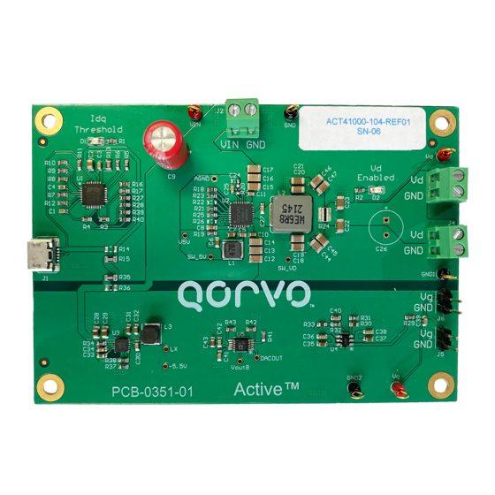
Figure 1. Reference Design Picture
www.qorvo.com
March 2022 Rev 1.0 | Subject to change without notice
1 of 22
Advertisement
Table of Contents

Summary of Contents for Qorvo ACT41000-104-REF01
- Page 1 RF PA gate voltage to set the required Idq bias current. This reference design demonstrates how Qorvo’s ACT41000 simplifies RF PA system level design and cost. The design is specifically configured for the QPA2211, but it can be easily modified for many other RF PAs.
-
Page 2: Required Equipment
Digital Multi-meters (DMM) • Windows compatible PC with spare USB port • USB cable shown in Figure 3 Hardware Setup Figure 2. Reference Setup with QPA2211 www.qorvo.com March 2022 Rev 1.0 | Subject to change without notice 2 of 22... -
Page 3: Quick Start
6. If connecting an RF input source to the RF PA, ensure that it disabled. Figure 3. Board-USB-Laptop Connection GUI Setup 1. Refer to the end of this document for detailed instructions to install the ACT41000-104-REF01 GUI. www.qorvo.com March 2022 Rev 1.0 | Subject to change without notice... -
Page 4: Recommended Operating Conditions
USER’S GUIDE UG146 Recommended Operating Conditions The ACT41000-104-REF01 is designed for a 24V-40V input voltage. The maximum operating voltage is determined by the IC’s maximum input voltage rating of 40V. The minimum operating voltage is determined by the IC’s output voltage setting. - Page 5 USER’S GUIDE UG146 Figure 5. GUI Detailed Functional Buttons Figure 6. Bias Search Routine Flow Chart www.qorvo.com March 2022 Rev 1.0 | Subject to change without notice 5 of 22...
- Page 6 11. Select Step, the gate voltage step resolution. A smaller step results in a more accurate search result, but takes longer to find the required gate voltage. www.qorvo.com March 2022 Rev 1.0 | Subject to change without notice 6 of 22...
- Page 7 Modifications to Test a Different RF PA The ACT41000-104-REF01 default settings are compatible with the QPA2211. The design can be easily modified to support any other RF PAs with drain voltages up to 24V and drain currents up to 4A. Typically, only four modifications needed to test a different RF PA.
-
Page 8: Test Results
USER’S GUIDE UG146 Test Results www.qorvo.com March 2022 Rev 1.0 | Subject to change without notice 8 of 22... - Page 9 USER’S GUIDE UG146 www.qorvo.com March 2022 Rev 1.0 | Subject to change without notice 9 of 22...
- Page 10 USER’S GUIDE UG146 Schematic Figure 9. Schematic Top Level www.qorvo.com March 2022 Rev 1.0 | Subject to change without notice 10 of 22...
- Page 11 USER’S GUIDE UG146 Figure 10. Schematic I2C Interface Controller www.qorvo.com March 2022 Rev 1.0 | Subject to change without notice 11 of 22...
- Page 12 USER’S GUIDE UG146 Figure 11. Schematic Vdrain Supply www.qorvo.com March 2022 Rev 1.0 | Subject to change without notice 12 of 22...
- Page 13 USER’S GUIDE UG146 Figure 12. Schematic Vgate Supply www.qorvo.com March 2022 Rev 1.0 | Subject to change without notice 13 of 22...
- Page 14 USER’S GUIDE UG146 Layout Figure 13. Assembly Layer www.qorvo.com March 2022 Rev 1.0 | Subject to change without notice 14 of 22...
- Page 15 USER’S GUIDE UG146 Figure 14. Layout Top Layer www.qorvo.com March 2022 Rev 1.0 | Subject to change without notice 15 of 22...
- Page 16 USER’S GUIDE UG146 Figure 15. Layout Layer 2 - GND www.qorvo.com March 2022 Rev 1.0 | Subject to change without notice 16 of 22...
- Page 17 USER’S GUIDE UG146 Figure 16. Layout Layer 3 www.qorvo.com March 2022 Rev 1.0 | Subject to change without notice 17 of 22...
- Page 18 USER’S GUIDE UG146 Figure 17. Layout Bottom Layer www.qorvo.com March 2022 Rev 1.0 | Subject to change without notice 18 of 22...
-
Page 19: Bill Of Materials
R42, R43 Res, 0Ω R13, R15, R35 0805 Standard Standard R14, R36 0805 Standard Standard R16, R18, R27, R28, Res, 0Ω 0603 Standard Standard R39, R40 www.qorvo.com March 2022 Rev 1.0 | Subject to change without notice 19 of 22... - Page 20 IC, AD5627RBRMZ-1REEL7 AD5627RBRMZ-1REEL7 Devices Inc Vd, Vg, VIN Test Point, Red KeyStone TESTPOINT 5000 GND, GND1, GND2 Test Point, Black KeyStone TESTPOINT 5001 PCB, ACT41000-104-REF01 PCB-0351-01 www.qorvo.com March 2022 Rev 1.0 | Subject to change without notice 20 of 22...
-
Page 21: Gui Installation
USER’S GUIDE UG146 GUI Installation 1. Get GUI files from the Qorvo website 2. Plug the USB-TO-I2C cable into a free USB port. 3. Follow the instructions in the “How to install driver for dongle” folder. 4. Double click on the ACT41000 Power Amplifier Rev0.6.exe to start the ACT41000EVK 104 REF01. -
Page 22: Contact Information
Data Sheet Information is suitable for use in a particular application. © 2020 Qorvo US, Inc. All rights reserved. This document is subject to copyright laws in various jurisdictions worldwide and may not be reproduced or distributed, in whole or in part, without the express written consent of Qorvo US, Inc.