Table of Contents
Advertisement
Quick Links
SERVICE MANUAL
/ Video Cassette Recorder
The above models are classified as green products (*1), as indicated by the underlined serial
numbers. This Service Manual describes replacement parts for the green products. When
repairing these green product(s), use the part(s) described in this manual and lead-free solder (*2).
For (*1) and (*2), see the next page.
TOSHIBA CORPORATION 2006
PAL
PAL
SECAM
I/
VCR
REC
ON / STANDBY
FILE NO. 810-200662GR
®
HDD & DVD
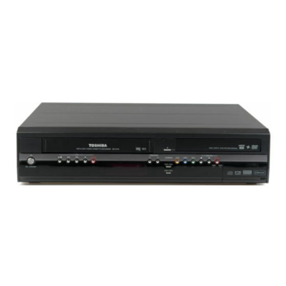
RD-XV45KE
RD-XV45KB
RD-XV45KF
HDD/DVD
PROGRAM
DUBBING
VCR
HDD
DVD
REC
VCR
DVD
HDD
DVD
HDD
DVD
Published in Japan, July 2007 GREEN
REVISED: 03
Advertisement
Chapters
Table of Contents

Related Manuals for Toshiba RD-XV45KE


Summary of Contents for Toshiba RD-XV45KE
- Page 1 This Service Manual describes replacement parts for the green products. When repairing these green product(s), use the part(s) described in this manual and lead-free solder (*2). For (*1) and (*2), see the next page. TOSHIBA CORPORATION 2006 Published in Japan, July 2007 GREEN...
- Page 2 Hazardous Substances. From July 1, 2006, the RoHS Directive will prohibit any marketing of new products containing the restricted substances. Increasing attention is given to issues related to the global environmental. Toshiba Corporation recognizes environmental protection as a key management tasks, and is doing its utmost to enhance and improve the quality and scope of its environmental activities.
-
Page 3: Table Of Contents
MAIN SECTION HDD & DVD / Video Cassette Recorder RD-XV45KE/RD-XV45KB/RD-XV45KF Main Section I Specifications I Preparation for Servicing I Adjustment Procedures I Schematic Diagrams I BOARD’s I Exploded Views I Parts List TABLE OF CONTENTS Specifications ................1-1-1 Laser Beam Safety Precautions. -
Page 4: Specifications
435 x 99.5 x 380mm Operating temperature 5ºC to 40ºC Operating humidity Less than 80% (no condensation) TV format PAL BG / DK + SECAM BG / DK (RD-XV45KE) PAL - I (RD-XV45KB) SECAM LL , PAL B / G (RD-XV45KF) Recording Recording format... -
Page 5: Laser Beam Safety Precautions
LASER BEAM SAFETY PRECAUTIONS This DVD player uses a pickup that emits a laser beam. Do not look directly at the laser beam coming from the pickup or allow it to strike against your skin. The laser beam is emitted from the location shown in the figure. When checking the laser diode, be sure to keep your eyes at least 30 cm away from the pickup lens when the diode is turned on. -
Page 6: Important Safety Precautions
IMPORTANT SAFETY PRECAUTIONS Product Safety Notice K. Crimp type wire connector The power transformer uses crimp type connectors Some electrical and mechanical parts have special which connect the power cord and the primary side safety-related characteristics which are often not evi- of the transformer. - Page 7 Safety Check after Servicing Examine the area surrounding the repaired location for damage or deterioration. Observe that screws, Chassis or Secondary Conductor parts, and wires have been returned to their original positions. Afterwards, do the following tests and con- Primary Circuit firm the specified values to verify compliance with safety standards.
-
Page 8: Standard Notes For Servicing
STANDARD NOTES FOR SERVICING NOTE: BOARD MEANS PRINTED CIRCUIT BOARD. Circuit Board Indications Pb (Lead) Free Solder 1. The output pin of the 3 pin Regulator ICs is When soldering, be sure to use the Pb free solder. indicated as shown. How to Remove / Install Flat Pack-IC Top View Bottom View... - Page 9 3. The flat pack-IC on the BOARD is affixed with With Soldering Iron: glue, so be careful not to break or damage the foil 1. Using desoldering braid, remove the solder from of each pin or the solder lands under the IC when all pins of the flat pack-IC.
- Page 10 With Iron Wire: 2. Installation 1. Using desoldering braid, remove the solder from 1. Using desoldering braid, remove the solder from all pins of the flat pack-IC. When you use solder the foil of each pin of the flat pack-IC on the flux which is applied to all pins of the flat pack-IC, BOARD so you can install a replacement flat pack- you can remove it easily.
- Page 11 Instructions for Handling Semi- conductors Electrostatic breakdown of the semi-conductors may occur due to a potential difference caused by electrostatic charge during unpacking or repair work. 1. Ground for Human Body Be sure to wear a grounding band (1 MΩ) that is properly grounded to remove any static electricity that may be charged on the body.
-
Page 12: Handling Precautions For Hdd
HANDLING PRECAUTIONS FOR HDD CAUTION: 4. OTHERS a. Be careful so as not to do the followings. 1. SHOCK Otherwise, HDD might be damaged. a. Exposing HDD to shock may be the biggest - DO NOT disassemble HDD. damaging factor. Please note that HDD is easily - When handling HDD, be sure to hold both sides damaged even if dropped from any height. -
Page 13: Preparation For Servicing
PREPARATION FOR SERVICING How to Enter the Service Mode About Optical Sensors Caution: An optical sensor system is used for the Tape Start and End Sensors on this equipment. Carefully read and follow the instructions below. Otherwise the unit may operate erratically. What to do for preparation Insert a tape into the Deck Mechanism Assembly and press [ O ] (VCR) button. -
Page 14: Cabinet Disassembly Instructions
CABINET DISASSEMBLY INSTRUCTIONS NOTE: BOARD MEANS PRINTED CIRCUIT BOARD. 1. Disassembly Flowchart REMOVAL This flowchart indicates the disassembly steps to gain REMOVE/*UNHOOK/ LOC. PART Fig. access to item(s) to be serviced. When reassembling, UNLOCK/RELEASE/ Note follow the steps in reverse order. Bend, route, and UNPLUG/DESOLDER dress the cables as they were originally. - Page 15 Reference Notes 1. Locking Tabs (L-1) and (L-2) are fragile. Be careful (S-3B) not to break them. [3] Front Bracket 1-1. Remove Screw (S-2). (S-3B) 1-2. Release five Locking Tabs (L-1). (S-3) Front 1-3. Release three Locking Tabs (L-2) and Support remove the Front Assembly.
- Page 16 CN3002 [14] BOARD SWITCH CN3001 (S-7) Desolder [9] BOARD ATA [15] BOARD FRONT JACK (S-14) (S-12) [7] HDD Unit CL1001 (S-7) (S-13) HDD Rubber CN3001 [8] HDD Support [13] BOARD POWER HDD Rubber SUPPLY Insulation Sheet (S-8) (S-8) Fig. D6 [6] HDD Bracket (S-16) (S-15)
- Page 17 Cylinder Assembly FE Head ACE Head Assembly SW507 LD-SW [17] Deck Assembly [18] BOARD [19] BOARD [18] BOARD POWER POWER SWITCH [17] Deck Assembly Cam Gear Hole (S-18) Shaft [18] BOARD POWER Desolder (S-19) Hole LD-SW [18] BOARD POWER Lead with blue stripe From FE Head...
- Page 18 (S-20) [20] Deck Pedestal (S-20) [21] Front Bracket R [22] Bracket R (S-22) (S-21) Fig. D9 3. How to Eject Manually Note: When rotating the gear, be careful not to damage the gear. 1. Remove the Cover Top. 2. Rotate the gear in the direction of the arrow manually as shown below. View for A Rotate this gear in the direction of the arrow...
-
Page 19: Electrical Adjustment Instructions
ELECTRICAL ADJUSTMENT INSTRUCTIONS NOTE: BOARD MEANS PRINTED CIRCUIT BOARD. NOTE: 1.Electrical adjustments are required after replacing circuit components and certain mechanical parts. It is important to do these adjustments only after Figure 1 all repairs and replacements have been com- pleted. -
Page 20: How To Self-Check And Initialize The Hdd & Dvd/Vcr
HOW TO SELF-CHECK AND INITIALIZE THE HDD & DVD/VCR 1. Turn on the HDD & DVD/VCR. 2. To put the HDD & DVD/VCR into the HDD mode, press [HDD] on the remote control unit. 3. To put the HDD & DVD/VCR into the self-check mode, after pressing [VARIABLE SKIP] button, press the [3], [6], and [9] buttons on the remote control in that order within three seconds. - Page 21 Table 2: Indication of DVD self-check (*7) INDICATION DESCRIPTION Connection of DVD is normal. NOT FOUND DVD drive cannot be found. FFC cable (connecting to CN401) between the DVD drive and the DVD/HDD MAIN BOARD CABLE ERROR is not connected correctly. Table 3: Indication of HDD self-check (*8) INDICATION DESCRIPTION...
-
Page 22: Firmware Renewal Mode
FIRMWARE RENEWAL MODE 1. Update Contents 4. Load the update disc. The TV screen will display Fig. c. Item Status - If the update disc contains only a single file, the update will initiate automatically when the disc is Update B/E FIRMWARE inserted. - Page 23 The status displayed in *2 is as shown below. 3. How to Verify the Firmware Version Display Status 1. Turn the power on and remove the disc in the tray. Loading F/W from Update Disc or EXECUTING writing to Flash memory 2.
-
Page 24: Troubleshooting
TROUBLESHOOTING NOTE: BOARD MEANS PRINTED CIRCUIT BOARD. 1 Power Supply Section FLOW CHART NO.1 The power cannot be turned on. See FLOW CHART No.2 <The fuse blows out.> Is the fuse normal? Is normal state restored when once unplugged Check for lead or short-circuiting of primary power cord is plugged again after several seconds. - Page 25 FLOW CHART NO.6 EV+44V is not outputted. Check D013, C013, and their periphery, and Is 44V voltage supplied to the emitter of Q1509? service it if defective. Is the "L" pulse (approximately 0V) inputted to Is the "H" pulse (approximately 5V) inputted to the base of Q1509? the base of Q1510? Replace Q1509.
- Page 26 FLOW CHART NO.10 HDD+5V is not outputted. Is 5V voltage supplied to the emitter of Q1102? Check D016, D1032, D1102, C1104, C1105 and their periphery, and service it if defective. Is the "L" pulse outputted to the collector of Q1104? Check Q1104, D1117 and their periphery, and service it if defective.
- Page 27 2 HDD/DVD Section FLOW CHART NO.1 The key operation is not functioning. Are the contact point and the installation state of Re-install the key switches correctly or replace the poor switch. the key switches normal? Is the control voltage normally inputted into Check the key switches and their periphery, and Pin(1,2) of IC1504? service it if defective.
- Page 28 FLOW CHART NO.4 VIDEO E-E does not appear normally. Are the video signals inputted to each pin of Check the line between video input terminal and IC1506? each pin of IC1506. → JK1504 IC1506 16PIN VIDEO-IN 1 (AV1) IC1506 16PIN VIDEO-IN 1 (AV1) →...
- Page 29 Replace the DVD MECHANISM & DVD MAIN Are the video signals outputted to each pin of BOARD ASSEMBLY. CN1504? CN1504 7PIN VIDEO-Y(I/P)-OUT CN1504 1PIN VIDEO-Y(I)-OUT CN1504 3PIN VIDEO-Cr/Pr-OUT CN1504 5PIN VIDEO-Cb/Pb-OUT CN1504 9PIN VIDEO-C-OUT Are the video signals shown above inputted into Check the line between each pin of CN1504 and each pin of IC1506? each pin of IC1506, and service it if defective.
- Page 30 FLOW CHART NO.5 Picture does not appear normally. Set the disc on the disc tray, and playback it. (DVD MODE) Or, playback by selecting the picture in HDD top menu. (HDD MODE) Replace the DVD MECHANISM & DVD MAIN Are the video signals outputted to each pin of BOARD ASSEMBLY.
- Page 31 FLOW CHART NO.6 Audio E-E does not appear normally. Check the line between audio input terminal and each pin of IC1506, and service it if defective. No (Rear →JK1504 IC1506 93,94PIN AUDIO-IN1 (AV1) or Front →JK3002, IC1506 91,92PIN AUDIO-IN1 (FRONT) input) Are the audio signals inputted to each pin of JK3003...
- Page 32 Replace the DVD MECHANISM & DVD MAIN Are the analog audio signals outputted to each pin BOARD ASSEMBLY. of CN1504? CN1504 17PIN AUDIO (L)-OUT CN1504 15PIN AUDIO (R)-OUT Are the analog audio signals inputted to each pin Check each line between each pin of CN1504 and each pin of IC1505, and service it if defective.
- Page 33 FLOW CHART NO.7 Audio is not outputted during playback. Set the disc on the disc tray, and playback it. (DVD MODE) Or, playback by selecting the picture in HDD top menu. (HDD MODE) Replace the DVD MECHANISM & DVD MAIN Are the analog audio signals outputted to each pin BOARD ASSEMBLY.
- Page 34 3 VCR Section FLOW CHART NO.1 The key operation is not functioning. Are the contact point and the installation state of Re-install some key switches correctly or the key switches normal? replace some key switches. Check the key switches and their periphery, and Is the control voltage normally inputted into service it if defective.
- Page 35 FLOW CHART NO.3 Cassette tape can not be loaded. When loading a cassette tape, on Pin(10) of Check the line between the start sensor and IC501, does the "L" pulse switch to the "H" pulse? Pin(10) of IC501, and service it if defective. When loading a cassette tape, is the specified Replace the Capstan Motor Unit.
- Page 36 FLOW CHART NO.6 Capstan Motor does not rotate. Is 5V voltage supplied to Pin(2) of CN502? Check the P-ON+5V line and service it if defective. Is over approximately 2.6V voltage supplied to Check the line between Pin(5) of CN502 and Pin(5) of CN502? Pin(76) of IC501, and service it if defective.
- Page 37 FLOW CHART NO.10 Video E-E does not appear. Are the video signals inputted to each pin of Check the line between video input terminal and IC1506? each pin of IC1506. → JK1504 IC1506 16PIN VIDEO-IN 1 (AV1) IC1506 16PIN VIDEO-IN 1 (AV1) →...
- Page 38 Are the video signals outputted to each pin of IC1506? Is 5V voltage supplied to Pin(27,29,47,63) of IC1506? IC1506 30PIN VIDEO-OUT 1 (AV1) IC1506 22PIN VIDEO-OUT 2 (AV2) Check the AL+5V(2) line Replace IC1506. and service it if defective. Are the video signals outputted to the specific output terminal? Check the periphery of JK1504 from Pin(30) of Are the composite video signals outputted to the...
- Page 39 Check the line between Pin(3,13) of IC1501 and Is the audio signal inputted to Pin(4,50) of IC451? Pin(4,50) of IC451, and service it if defective. Is the 5V voltage supplied to Pin(16,32,35,36,46,55) of Check the circuit of AL+5V, P-ON+5V and IC451, or the 9V voltage supplied to Pin(69) of IC451? P-ON+9V, and service it if defective.
- Page 40 FLOW CHART NO.12 Hi-Fi audio can not be recorded normally. (E-E mode is normal.) Is the REC FM signal outputted to Pin(26) of IC451? Replace IC451. Check the line between Pin(8) of CN251 and Is the line between Pin(8) of CN251 and Pin(26) of IC451, and service it if defective.
- Page 41 FLOW CHART NO.15 Hi-Fi audio can not be playbacked normally in the linear audio mode. (E-E mode is normal.) Is the audio signal outputted to Pin(11) of IC301? Is the audio signal supplied to Pin(5) of IC301? Check the line between Pin(11) of Replace IC301 and Pin(80) of IC451, and IC301.
-
Page 42: Function Indicator Symbols
FUNCTION INDICATOR SYMBOLS < VCR Section > Note: If a mechanical malfunction occurs, the power is turned off. The following symbols will appear on the display. Status Display When reel or capstan mechanism is not functioning correctly When tape loading mechanism is not functioning correctly “W”... - Page 43 < DVD/HDD Section > Note: If an error occurs, a message with the error number appears on the screen. Error message Recording Error Error No. 02-50 Message Error No. Error Description Error Example Renewal error at This code is output when there is a control information writing failure 04-50 ejecting disc due to tray being open during writing or disc loading.
-
Page 44: Block Diagrams
(SERVO/SYSTEM CONTROL) BOARD POWER TP501 LD-SW ACE HEAD ASSEMBLY CN504 AL+5V LD-SW SENS-INH Model Mark CTL(+) KEY- 2 8 CONTROL CTL(+) RD-XV45KE HEAD CTL(-) KEY- 1 CTL(-) KEY SWITCH RD-XV45KB ST-S REC-SAF-SW 31 AL+5V RD-XV45KF END-S SW506 TP502 T-REEL REC-SAFETY... - Page 45 Sub System Control Block Diagram NOTE: BOARD MEANS PRINTED CIRCUIT BOARD. IC1504 (SUB MICRO CONTROLLER) REG-CONT IC1502 REG-CONT PWR -SW Q1527 PW-SW TO SUB LOW-POW RESET RESET EV+3.3V LOW-POW POWER SUPPLY FAN-LOCK BLOCK DIAGRAM FAN-LOCK FAN-CONT1 FAN-CONT1 P-DOWN BUP+3.3V Q1528 TIMER+5V C1547 (BACKUP CAPACITOR)
- Page 46 Digital Signal Process Block Diagram NOTE: BOARD MEANS PRINTED CIRCUIT BOARD. REC VIDEO SIGNAL PB VIDEO SIGNAL REC AUDIO SIGNAL PB AUDIO SIGNAL CN3002 CN3001 CN201 HARD DISK IC101 IC201 IC601 (MPEG2 AV CODEC) DRIVE CN601 VIDEO-Y/CVBS-IN BOARD ERROR AMP VIDEO-C-IN TO VIDEO VIDEO-Y(I/P)-OUT...
- Page 47 Video Selector Block Diagram NOTE: BOARD MEANS PRINTED CIRCUIT BOARD. REC VIDEO SIGNAL PB VIDEO SIGNAL IC1506 (VIDEO SELECTOR) BOARD BOARD REAR JACK POWER Q2001 JK2001 CN2001 CN1507 VIDEO OUT2 BUFFER VIDEO-OUT2 DRIVER VIDEO-G VIDEO-G-IN JK2001 CN1507 CN2001 VIDEO-B VIDEO-B-IN VIDEO-IN2 VIDEO VIDEO-R...
- Page 48 Video Block Diagram NOTE: BOARD MEANS PRINTED CIRCUIT BOARD. REC-VIDEO SIGNAL PB-VIDEO SIGNAL MODE: SP/REC Comparison Chart of Models & Marks Model Mark RD-XV45KE IC501 (OSD) RD-XV45KB IIC-BUS SCL TO SERVO/SYSTEM RD-XV45KF CHARACTER CONTROL BLOCK IIC-BUS SDA DIAGRAM COLOR Q402...
- Page 49 Audio Selector Block Diagram NOTE: BOARD MEANS PRINTED CIRCUIT BOARD. REC AUDIO SIGNAL PB AUDIO SIGNAL BOARD REAR JACK IC1506(AUDIO SELECTOR) JK2001 BOARD POWER CN1507 CN2001 AUDIO(L)-IN2 AUDIO(L)-IN2 TO SUB SYSTEM AUDIO(R)-IN2 AUDIO(R)-IN2 CONTROL AUDIO(L)-OUT2 AUDIO(L)-OUT2 BLOCK DIAGRAM AUDIO(R)-OUT2 AUDIO(R)-OUT2 AUDIO-MUTE MUTE-ON MUTE-ON...
- Page 50 Audio Block Diagram NOTE: BOARD MEANS PRINTED CIRCUIT BOARD. PB-AUDIO SIGNAL REC-AUDIO SIGNAL Mode : SP/REC BOARD POWER N-A-PB TO Hi-Fi AUDIO N-A-REC BLOCK DIGRAM IC301 (AUDIO SIGNAL PROCESS) PB-ON LINE MUTE (DECK ASSEMBLY) SP/LP-ON ACE HEAD ASSEMBLY REC-ON Q404 CN504 AUDIO 4 AUDIO-PB/REC...
- Page 51 Hi-Fi Audio Selector Block Diagram NOTE: BOARD MEANS PRINTED CIRCUIT BOARD. PB-AUDIO SIGNAL REC-AUDIO SIGNAL Mode : SP/REC BOARD POWER VCR-AUDIO-IN(L) TO AUDIO VCR-AUDIO-IN(R) SELECTOR BLOCK DIAGRAM IC451 ( Hi-Fi AUDIO PROCESS) R-CH IIC-BUS SDA SERIAL COMP NOISE DATA IIC-BUS SCL DECODER R-CH SERVO/ SYSTEM...
- Page 52 Power Supply Block Diagram NOTE: BOARD MEANS PRINTED CIRCUIT BOARD. CAUTION ! CAUTION ! NOTE: Fixed voltage (or Auto voltage selectable) power supply circuit is used in this unit. For continued protection against fire hazard, The voltage for parts in hot circuit is measured using If Main Fuse (F1001) is blown , check to see that all components in the power supply replace only with the same type fuse.
- Page 53 Sub Power Supply Block Diagram NOTE: BOARD MEANS PRINTED CIRCUIT BOARD. CN1501 1 AL-30V 2 AL+44V Q1509 3,4 AL+16.3V P-ON+15V 7,8 AL+12V 14 P-ON+9V(1) Q1510 15,16 P-ON+5V(A) 17,18 AL+5V(3) POWER SUPPLY Q1501 BLOCK DIAGRAM 22 AL+5V (CL1001) AL+16V/+12V 23 F1 24 F2 Q1502 25 REG-CONT...
-
Page 54: Schematic Diagrams / Board's And Test Points
SCHEMATIC DIAGRAMS / BOARD’S AND TEST POINTS NOTE: BOARD MEANS PRINTED CIRCUIT BOARD. Standard Notes WARNING Many electrical and mechanical parts in this chassis have special characteristics. These characteristics often pass unnoticed and the protection afforded by them cannot necessarily be obtained by using replacement components rated for higher voltage, wattage, etc. - Page 55 LIST OF CAUTION, NOTES, AND SYMBOLS USED IN THE SCHEMATIC DIAGRAMS ON THE FOLLOWING PAGES: 1. CAUTION: FOR CONTINUED PROTECTION AGAINST FIRE HAZARD, REPLACE ONLY WITH THE SAME TYPE FUSE. 2. CAUTION: Fixed Voltage (or Auto voltage selectable) power supply circuit is used in this unit. If Main Fuse (F1001) is blown, first check to see that all components in the power supply circuit are not defective before you connect the AC plug to the AC power supply.
- Page 56 POWER 1/10 Schematic Diagram < VCR Section > NOTE: BOARD MEANS PRINTED CIRCUIT BOARD. Comparison Chart of Models and Marks MODEL MARK RD-XV45KE RD-XV45KB RD-XV45KF 1-14-3 E439ASCP1...
- Page 57 POWER 2/10 & SENSOR Schematic Diagram < VCR Section > NOTE: BOARD MEANS PRINTED CIRCUIT BOARD. FL601 MATRIX CHART TIME P-SCAN SHIFT TIME P-SCAN SHIFT CD R 1-14-4 E439ASCP2...
- Page 58 POWER 3/10 Schematic Diagram < VCR Section > NOTE: BOARD MEANS PRINTED CIRCUIT BOARD. Comparison Chart of Models and Marks MODEL MARK RD-XV45KE RD-XV45KB RD-XV45KF 1-14-5 E439ASCP3...
- Page 59 POWER 4/10 Schematic Diagram < VCR Section > NOTE: BOARD MEANS PRINTED CIRCUIT BOARD. Comparison Chart of Models and Marks MODEL MARK RD-XV45KE RD-XV45KB RD-XV45KF 1-14-6 E439ASCP4...
- Page 60 You can choose either Group. The difference between Group A and Group B is shown below. Group A Group B R3112N191A-TR-FA IC1502A ---------- /BU4219G-TR IC1502B ---------- PST3619NR C1549A 0.015 ---------- C1549B ---------- Comparison Chart of Models and Marks MODEL MARK RD-XV45KE RD-XV45KB RD-XV45KF 1-14-7 E439ASCP5...
- Page 61 POWER 6/10 Schematic Diagram < VCR Section > NOTE: BOARD MEANS PRINTED CIRCUIT BOARD. 1-14-8 E439ASCP6...
- Page 62 POWER 7/10 Schematic Diagram < VCR Section > NOTE: BOARD MEANS PRINTED CIRCUIT BOARD. Comparison Chart of Models and Marks MODEL MARK RD-XV45KE RD-XV45KB RD-XV45KF 1-14-9 E439ASCP7...
- Page 63 POWER 8/10 Schematic Diagram < VCR Section > NOTE: BOARD MEANS PRINTED CIRCUIT BOARD. 1-14-10 E439ASCP8...
- Page 64 POWER 9/10 Schematic Diagram < VCR Section > NOTE: BOARD MEANS PRINTED CIRCUIT BOARD. 1-14-11 E439ASCP9...
- Page 65 POWER 10/10 Schematic Diagram < VCR Section > NOTE: BOARD MEANS PRINTED CIRCUIT BOARD. 1-14-12 E439ASCP10...
- Page 66 POWER SUPPLY Schematic Diagram < VCR Section > NOTE: BOARD MEANS PRINTED CIRCUIT BOARD. CAUTION ! CAUTION ! NOTE: Fixed voltage (or Auto voltage selectable) power supply circuit is used in this unit. For continued protection against fire hazard, The voltage for parts in hot circuit is measured using If Main Fuse (F1001) is blown , check to see that all components in the power supply replace only with the same type fuse.
- Page 67 FRONT JACK & SWITCH Schematic Diagram < VCR Section > NOTE: BOARD MEANS PRINTED CIRCUIT BOARD. 1-14-14 E439ASCFJ...
- Page 68 REAR JACK Schematic Diagram < VCR Section > ATA Schematic Diagram < DVD/HDD Section > NOTE: BOARD MEANS PRINTED CIRCUIT BOARD. E439ASCRJ E439ASCAT 1-14-15...
- Page 69 AFV Schematic Diagram < VCR Section > NOTE: BOARD MEANS PRINTED CIRCUIT BOARD. Comparison Chart of Models and Marks MODEL MARK RD-XV45KE RD-XV45KB RD-XV45KF 1-14-16 E439ASCAFV...
- Page 70 DVD/HDD MAIN 1/6 Schematic Diagram < DVD/HDD Section > NOTE: BOARD MEANS PRINTED CIRCUIT BOARD. 1-14-17 E439ASCD1...
- Page 71 DVD/HDD MAIN 2/6 Schematic Diagram < DVD/HDD Section > NOTE: BOARD MEANS PRINTED CIRCUIT BOARD. 1-14-18 E439ASCD2...
- Page 72 DVD/HDD MAIN 3/6 Schematic Diagram < DVD/HDD Section > NOTE: BOARD MEANS PRINTED CIRCUIT BOARD. 1-14-19 E439ASCD3...
- Page 73 DVD/HDD MAIN 4/6 Schematic Diagram < DVD/HDD Section > NOTE: BOARD MEANS PRINTED CIRCUIT BOARD. 2 NOTE: The order of pins shown in this diagram is different from that of actual IC601. IC601 is divided into six and shown as IC601 (1/6) ~ IC601 (6/6) in this DVD/HDD Main Schematic Diagram Section. 1-14-20 E439ASCD4...
- Page 74 DVD/HDD MAIN 5/6 Schematic Diagram < DVD/HDD Section > NOTE: BOARD MEANS PRINTED CIRCUIT BOARD. 2 NOTE: The order of pins shown in this diagram is different from that of actual IC601. IC601 is divided into six and shown as IC601 (1/6) ~ IC601 (6/6) in this DVD/HDD Main Schematic Diagram Section. 1-14-21 E439ASCD5...
- Page 75 DVD/HDD MAIN 6/6 Schematic Diagram < DVD/HDD Section > NOTE: BOARD MEANS PRINTED CIRCUIT BOARD. 2 NOTE: The order of pins shown in this diagram is different from that of actual IC601. IC601 is divided into six and shown as IC601 (1/6) ~ IC601 (6/6) in this DVD/HDD Main Schematic Diagram Section. 1-14-22 E439ASCD6...
- Page 76 BOARD POWER Top View NOTE: BOARD MEANS PRINTED CIRCUIT BOARD. BOARD SENSOR Top View TO BOARD SENSOR (END-SENSOR) TP504 TP301 J340 RF-SW C-PB JK2-V-OUT BHF300F01012A BHF300F01012B TO BOARD SENSOR (START-SENSOR) 1-14-23 BE434AF01015A...
- Page 77 BOARD POWER Bottom View NOTE: BOARD MEANS PRINTED CIRCUIT BOARD. PIN 30 OF PIN 56 OF IC1506 IC301 PIN 3 OF CN1504 PIN 5 OF CN1504 PIN 7 OF CN1504 PIN 9 OF CN1504 PIN 17 OF CN1504 WF10 PIN 30 OF CN1501 1-14-24 BE434FA01015A...
- Page 78 BOARD POWER SUPPLY Top View NOTE: BOARD MEANS PRINTED CIRCUIT BOARD. Because a hot chassis ground is present in the power CAUTION ! CAUTION ! supply circut, an isolation transformer must be used. For continued protection against fire hazard, Fixed voltage (or Auto voltage selectable) power supply circuit is used in this unit. Also, in order to have the ability to increase the input replace only with the same type fuse.
- Page 79 BOARD POWER SUPPLY Bottom View NOTE: BOARD MEANS PRINTED CIRCUIT BOARD. CAUTION ! Because a hot chassis ground is present in the power CAUTION ! supply circut, an isolation transformer must be used. For continued protection against fire hazard, Fixed voltage (or Auto voltage selectable) power supply circuit is used in this unit. Also, in order to have the ability to increase the input replace only with the same type fuse.
- Page 80 BOARD FRONT JACK Top View NOTE: BOARD MEANS PRINTED CIRCUIT BOARD. BOARD SWITCH BOARD SWITCH Top View Bottom View BOARD FRONT JACK Bottom View BE434AF01022B BE434AF01022C 1-14-27...
- Page 81 BOARD REAR JACK Top View BOARD REAR JACK Bottom View NOTE: BOARD MEANS PRINTED CIRCUIT BOARD. BE434AF01022D BOARD POWER SWITCH BOARD POWER SWITCH BOARD ATA Top View BOARD ATA Bottom View Top View Bottom View BE434AF01015B BE4340F01032 1-14-28...
- Page 82 BOARD AFV Top View BOARD AFV Bottom View NOTE: BOARD MEANS PRINTED CIRCUIT BOARD. 1-14-29 BE6800F01091...
-
Page 83: Waveforms
WAVEFORMS NOTE: Input: COLOR BAR SIGNAL (WITH 1KHz AUDIO SIGNAL) Pin 56 of IC301 Pin 9 of CN1504 Pin 17 of CN1504 V-OUT E-E 0.2V 20μs VIDEO-C 0.2V 20μs AUDIO(L)-OUT 0.5ms Pin 56 of IC301 UPPER Pin 30 of IC1506 Pin 30 of CN1501 TP504 WF10... -
Page 84: Wiring Diagram
WIRING DIAGRAM NOTE: BOARD MEANS PRINTED CIRCUIT BOARD. REAR CN1501 DIGITAL AUDIO OUT AL-30V 1 S-VIDEO AUDIO(L) AUDIO(R) ANT-IN -OUT -OUT AL+44V 2 COAXIAL AL+16.3V 3 (DECK ASSEMBLY) AL+16.3V 4 JK1504 GND 5 (AV1) GND 6 ACE HEAD AL+12V 7 ASSEMBLY AL+12V 8 JK2201... - Page 85 WIRING DIAGRAM NOTE: BOARD MEANS PRINTED CIRCUIT BOARD. DVD MECHANISM & DVD/HDD MAIN BOARD UNIT CN501 CN1001 CL1001 DVD MECHANISM CN1001 CN401 SPDIF SPDIF AV-30V 1 18 VH- CN1003 AL+44V 2 17 HW- AL+16.3V 3 SLED 16 HW+ EV+10.5V EV+10.5V AL+16.3V 4 SENSOR 15 HV-...
-
Page 86: Ic Pin Function Descriptions
Signal Mark Function Name Comparison Chart of Models and Marks Not Used Model Mark Not Used RD-XV45KE Not Used RD-XV45KB RD-XV45KF Not Used Recording Safety SW IC501( SERVO / SYSTEM CONTROL IC ) IN REC-SAF- Detect (With Record tab=”L”/ With out Record Signal tab=”H”) - Page 87 Signal Signal Mark Function Mark Function Name Name Capstan Motor Rotation OUT C-POW-SW Capstan Power IN C-FG Detection Pulse Switching Signal AMPVss AMPVss Not Used IN SECAM-H SECAM Mode at High Drum Motor Phase/ Not Used IN D-PFG Frequency Generator Special playback = "H"...
- Page 88 IC612 (FRONT PANEL CONTROL) Signal Function Name IN CLK Clock Input IN STB Serial Interface Strobe Not Used Not Used Power Supply OUT a OUT b OUT c 10 OUT d Segment Output 11 OUT e IN f IN g 14 OUT h Pull Down Level 16 OUT i...
-
Page 89: Lead Identifications
LEAD IDENTIFICATIONS KRA103M-AT/P 2SC2120-(Y)(TE2 F T) S2Y52 KTC2026-Y/P 2SK3798(Q) KRA104M-AT/P KTC3203-Y-AT/P KRC103M-AT/P KTC3205-Y-AT/P KTA-1266-GR-AT/P KTC3198-Y-AT/P KTA1267Y-AT/P KTC3266-Y-AT/P KTA1281Y-AT/P KTC3193-Y-AT/P KTC3199-(BL,Y)-AT/P B C E B C E G D S E C B E C B PT204-6B-12 KRC106M-AT/P KIA431-AT/P UTC4580 PQ070XF01SZH KIA4558P/P 1: B 1: R... -
Page 90: Exploded Views
EXPLODED VIEWS Cabinet L-12 A,B,C,D,E See Electrical Parts List for parts with this mark. B-24 D,E,F ( P3-3 ) BOARD REAR JACK ( P5 ) B-10 BOARD AFV ( P4 ) JW2001 B-15 ( P6 ) BOARD SENSOR BOARD ATA B-31 B-19 BOARD POWER... - Page 91 Packing [RD-XV45KE/RD-XV45KF] [A,C] X-2A X-2C X-2D X-2B Comparison Chart of Models and Marks Model Mark RD-XV45KE RD-XV45KF 1-19-2 E439APEX...
- Page 92 Packing [RD-XV45KB] X-29 X-30 1-19-3 E439APEX...
-
Page 93: Mechanical Parts List
SCREW TAP TIGHT M3X5 Comparison Chart of Models and Marks BIND HEAD+BLK NI L-1F GBHC3050 SCREW TAP TIGHT M3X5 Model Mark BIND HEAD+BLK NI RD-XV45KE L-1G GBHC3050 SCREW TAP TIGHT M3X5 BIND HEAD+BLK NI RD-XV45KB L-3A GBHB3080 SCREW B-TIGHT M3X8... - Page 94 Loca- Mark TSB P/N Reference No. Description tion No. L-9Q 0VM412937A SCREW C-TIGHT M3X6 E5610UD L-9R GBJS3060 SCREW S-TIGHT M3X6 BIND HEAD+ L-10A 0VM413320A SCREW S-TIGHT 3X8 H9210UD L-10B 0VM413320A SCREW S-TIGHT 3X8 H9210UD L-10C 0VM413320A SCREW S-TIGHT 3X8 H9210UD L-10D 0VM413320A SCREW S-TIGHT 3X8...
-
Page 95: Electrical Parts List
CHIP CERAMIC CAP .(1608) B K 0.01μF/ Comparison Chart of Models and Marks C315 CHD1JK30B473 CHIP CERAMIC CAP .(1608) B K 0.047μF/ Model Mark RD-XV45KE C316 CE1JMAVSL1R0 ELECTROLYTIC CAP . 1μF/ RD-XV45KB 50V M H7 RD-XV45KF C317 CHD1JZ30F104 CHIP CERAMIC CAP .(1608) F Z 0.1μF/50V... - Page 96 Loca- Loca- Mark TSB P/N Reference No. Description Mark TSB P/N Reference No. Description tion No. tion No. C349 CE1JMAVSLR47 ELECTROLYTIC CAP . C455 CHD1JZ30F104 CHIP CERAMIC 0.47μF/50V M H7 CAP .(1608) F Z 0.1μF/50V C350 CCA1JZTFZ104 CERAMIC CAP .(AX) F Z C456 CE1CMAVSL100 ELECTROLYTIC CAP .
- Page 97 Loca- Loca- Mark TSB P/N Reference No. Description Mark TSB P/N Reference No. Description tion No. tion No. C509 CHD1JK30B102 CHIP CERAMIC C612 CHD1JK30B472 CHIP CERAMIC CAP .(1608) B K 1000pF/ CAP .(1608) B K 4700pF/ C510 CHD1JK30B472 CHIP CERAMIC C614 CHD1JZ30F104 CHIP CERAMIC...
- Page 98 Loca- Loca- Mark TSB P/N Reference No. Description Mark TSB P/N Reference No. Description tion No. tion No. If C1549B is 0.1μF, then IC1502B is PST3619NR. C1588 CE1JMASDL1R0 ELECTROLYTIC CAP . 1μF/ 50V M C1549B CHD1JK30B104 CHIP CERAMIC CAP .(1608) B K 0.1μF/50V C1589 CE1EMASDL4R7 ELECTROLYTIC CAP .
- Page 99 Loca- Loca- Mark TSB P/N Reference No. Description Mark TSB P/N Reference No. Description tion No. tion No. C1631 CE0KMASDL471 ELECTROLYTIC CAP . CN1503 JCFNG20JG022 FMN CONNECTOR SIDE 470μF/6.3V M 20P 20FMN-STRK- A(LF)(SN) C1632 CHD1JZ30F104 CHIP CERAMIC CAP .(1608) F Z 0.1μF/50V CN1504 JCFNG30JG020 FMN CONNECTOR TOP...
- Page 100 Loca- Loca- Mark TSB P/N Reference No. Description Mark TSB P/N Reference No. Description tion No. tion No. D1536 QDTA00MTZJ11 ZENER DIODE MTZJT- L501 LLAXKATTU101 INDUCTOR(100μH K) 7711A LAP02TA101K D1539 QDTZ001SS133 SWITCHING DIODE L502 JW5.0T BOARD JUMPER D0.6- 1SS133(T-77) P5.0 D1540 QDTZ001SS133 SWITCHING DIODE...
- Page 101 Loca- Loca- Mark TSB P/N Reference No. Description Mark TSB P/N Reference No. Description tion No. tion No. CHIP RES. 1/10W J 6.8k Ω Q1514 NQSYKTC3199P TRANSISTOR KTC3199-Y- R327 RRXAJR5Z0682 AT/P CHIP RES. 1/10W J 1k Ω R328 RRXAJR5Z0102 Q1515 NQSYKTC3199P TRANSISTOR KTC3199-Y- CHIP RES.
- Page 102 Loca- Loca- Mark TSB P/N Reference No. Description Mark TSB P/N Reference No. Description tion No. tion No. R525 RRXAJR5Z0394 CHIP RES. 1/10W J 390k R648 RCX4JATZ0102 CARBON RES. 1/4W J 1k Ω Ω CHIP RES. 1/10W J 560 Ω R526 RCX6JATZ0394 CARBON RES.
- Page 103 Loca- Loca- Mark TSB P/N Reference No. Description Mark TSB P/N Reference No. Description tion No. tion No. R1551 RCX4JATZ0391 CARBON RES. 1/4W J 390 R1617 RRXAZR5Z0000 CHIP RES.(1608) 1/10W 0 Ω Ω CHIP RES. 1/10W J 470 Ω CHIP RES. 1/10W J 6.8k Ω R1552 RRXAJR5Z0471 R1618...
- Page 104 Loca- Loca- Mark TSB P/N Reference No. Description Mark TSB P/N Reference No. Description tion No. tion No. CHIP RES. 1/10W J 1k Ω R1675 RRXAJR5Z0102 R1741 CHD1JJ3CH680 CHIP CERAMIC CAP .(1608) CH J 68pF/50V CHIP RES. 1/10W J 1k Ω R1676 RRXAJR5Z0102 CHIP RES.
- Page 105 BOARD POWER SWITCH Loca- Mark TSB P/N Reference No. Description tion No. Loca- Mark TSB P/N Reference No. Description C1034 CMA2AJS00393 FILM CAP .(P) 0.039μF/ tion No. 100V J ---------- BOARD POWER SWITCH C1035 CE0KMZADL332 ELECTROLYTIC CAP . (AV PCB B) 3300μF/6.3V SL Consists of the following: C1036...
- Page 106 Loca- Loca- Mark TSB P/N Reference No. Description Mark TSB P/N Reference No. Description tion No. tion No. D018 NDQZ000BA158 RECTIFIER DIODE BA158 D1133 QD1Z001SS400 SWITCHING DIODE 1SS400 D019 NDQZ000FR203 RECTIFIER DIODE FR203-B/P D1134 QD1Z001SS400 SWITCHING DIODE 1SS400 D020 JW5.0T BOARD JUMPER D0.6- P5.0 D1135...
- Page 107 Loca- Loca- Mark TSB P/N Reference No. Description Mark TSB P/N Reference No. Description tion No. tion No. CHIP RES. 1/10W J 4.7k Ω Q1105 NQSYKTC3199P TRANSISTOR KTC3199-Y- R1120 RRXAJR5Z0472 AT/P R1123 RCX4JATZ0112 CARBON RES. 1/4W J 1.1k Ω Q1106 NQSYKTC3266P TRANSISTOR KTC3266-Y- AT/P R1124...
- Page 108 Loca- Loca- Mark TSB P/N Reference No. Description Mark TSB P/N Reference No. Description tion No. tion No. ! F1001 CHIP RES. 1/10W J 1k Ω P000459950 PAGC20BW3162 FUSE T1.6AL/250V R3015 RRXAJR5Z0102 CHIP RES. 1/10W J 1.5k Ω FH1001 XH01Z00LY002 FUSE HOLDER MSF-015 R3016 RRXAJR5Z0152...
- Page 109 BOARD AFV Loca- Mark TSB P/N Reference No. Description tion No. Loca- C2007 CHD1JK30B222 CHIP CERAMIC CAP . B K Mark TSB P/N Reference No. Description tion No. 2200pF/50V C2008 CHD1JK30B102 CHIP CERAMIC P000472710 1VSA12639 BOARD AFV CAP .(1608) B K 1000pF/ P000473050 1VSA13522 BOARD AFV...
- Page 110 BOARD ATA Loca- Mark TSB P/N Reference No. Description tion No. P000472730 1VSA13582 BOARD ATA Consists of the following: CONNECTORS CN3001 JCYKC40JC002 IDC SOCKET 40PIN VT YKF43-0025 CN3002 JCFHD40HQ007 FPC/FFC CONNECTOR(40PIN) FH12-40S-0.5SH(89) 20060714 1-21-16 E439AEL...
- Page 111 DECK MECHANISM SECTION HDD & DVD / Video Cassette Recorder RD-XV45KE/RD-XV45KB/RD-XV45KF Deck Mechanism Section I Standard Maintenance I Mechanism Alignment Procedures I Disassembly / Assembly of Mechanism I Deck Exploded Views I Deck Parts List TABLE OF CONTENTS Standard Maintenance ..............2-1-1 Service Fixture and Tools.
-
Page 112: Standard Maintenance
STANDARD MAINTENANCE Service Schedule of Components This maintenance chart shows you the standard of replacement and cleaning time for each part. Because those may replace depending on environment and purpose for use, use the chart for reference. I: Replace h: Hours : Cleaning Deck Periodic Service Schedule... - Page 113 Cleaning Cleaning of ACE Head Clean the head with a cotton swab. Cleaning of Video Head Procedure Clean the head with a head cleaning stick or chamois 1.Remove the top cabinet. cloth. 2.Dip the cotton swab in 90% ethyl alcohol and clean Procedure the ACE Head.
-
Page 114: Service Fixture And Tools
SERVICE FIXTURE AND TOOLS J-1-1, J-1-2 Ref. No. Name Part No. Adjustment J-1-1 Alignment Tape FL6A Head Adjustment of ACE Head J-1-2 Alignment Tape FL6N8 Azimuth and X Value Adjustment of ACE Head / (2 Head model) Adjustment of Envelope Waveform FL6NS8 (4 Head model) Guide Roller Adj. -
Page 115: Mechanical Alignment Procedures
MECHANICAL ALIGNMENT PROCEDURES Explanation of alignment for the tape to correctly run B. Method to place the Cassette Holder in the tape- starts on the next page. Refer to the information below loaded position without a cassette tape on this page if a tape gets stuck, for example, in the 1. - Page 116 1. Tape Interchangeability Alignment Note: To do these alignment procedures, make sure that the Tracking Control Circuit is set to the preset position every time a tape is loaded or unloaded. (Refer to page 2-3-4, procedure 1-C, step 2.) Equipment required: Dual Trace Oscilloscope VHS Alignment Tape (FL6NS8) Guide Roller Adj.
- Page 117 1-A. Preliminary/Final Checking and 4. If creasing or snaking is apparent, adjust the Tilt Alignment of Tape Path Adj. Screw of the ACE Head. (Fig. M6) Purpose: To make sure that the tape path is well stabilized. Azimuth Adj. Screw Symptom of Misalignment: If the tape path is unstable, the tape will be damaged.
- Page 118 5. To shift the CTL waveform, press CH UP or CH either at the beginning or end of track as shown in DOWN button on the remote control unit. Then Fig. M10. make sure that the maximum output position of PB ±...
- Page 119 1-D. Azimuth Alignment of Audio/Con- 2. When the tape has been curled up or bent, turn the trol/ Erase Head alignment screw to adjust the height of REV Post. (Refer to Fig. M11 and M13.) Purpose: To correct the Azimuth alignment so that the Audio/ Control/Erase Head meets tape tracks properly.
-
Page 120: Disassembly/Assembly Procedures Of Deck Mechanism
DISASSEMBLY/ASSEMBLY PROCEDURES OF DECK MECHANISM Before following the procedures described below, be sure to remove the deck assembly from the cabinet. (Refer to CABINET DISASSEMBLY INSTRUCTIONS.) All the following procedures, including those for adjustment and replacement of parts, should be done in Eject mode;... - Page 121 REMOVAL INSTALLATION STEP START- REMOVE/*UNHOOK/ /LOC. PART ADJUSTMENT Fig. No. UNLOCK/RELEASE/ CONDITION UNPLUG/DESOLDER Loading Arm (SP) (+)Refer to Alignment DM2H, DM14H [34] [26] Assembly Sec.Page 2-5-1 Loading Arm (TU) (+)Refer to Alignment [35] [34] DM2H, DM14H Assembly Sec.Page 2-5-1 M Brake (TU) [36] [16],[26] DM1H, DM15H...
- Page 122 Top View [44] [45] [49] [46] [14] [13] [11] [15] [38] [10] [12] [37] [36] [43] [32] [41] [31] [40] [42] Fig. DM1H Bottom View [19] [35] [34] [25] [23] [24] [26] [27] [22] [28] [20] [33] Fig. DM2H 2-4-3 U29PHSDA...
- Page 123 (S-1) (S-1) (L-1) (L-3) (L-2) (S-1A) (P-1) Installation of [3] and [6] First, insert [6] diagonally in [3] as shown below. Then, install [6] in [3] while pushing (L-1) in the direction of the arrow. After installing [6] in [3], confirm that pin A of [3] enters hole A of [6] properly.
- Page 124 [11] (S-4A) (L-4) [49] (P-3) [13] [50] Removal of [11] [12] (L-12) 1) Remove screw (S-4A). 2) Unhook spring (P-2). [10] Release (L-4) while (P-2) holding [12] with a finger. Loosen a finger holding [12] and remove [11]. (S-2) Pin of [12] Pin of [10] Groove of [27] When reassembling [10] and...
- Page 125 Installation of [13] and [12] (S-5) [14] (S-6) [13] [15] Hook spring (P-3) up to [12] and [13], then install them to (P-3) the specified position so that [12] will be floated slightly while holding [12] and [13]. (Refer to Fig. A.) [12] Fig.
- Page 126 (C-1) turn [22] (S-8) [20] (L-6) [21] [19] Cap Belt Pin on [22] Installation position of Cap Belt [20] Cap Belt [27] Position of pin on [22] Fig. DM12H [19] View for A Fig. DM11H 2-4-7 U29PHSDA...
- Page 127 Installation of [26] [26] (C-3) Position of Mode Lever when installed Pin of [33] Pin of [37] (S-9) Pin of [36] (L-8) [23] (L-7) Bottom View [24] (C-5) [26] (C-4) (C-2) [28] [27] [25] [29] [30] Align [26] and [27] as shown. [27] First groove on [27] First tooth on [47]...
- Page 128 [38] [36] [43] (P-6) turn [39] (L-10) turn [42] turn [47] [48] Slide [37] Fig. DM17H (C-7) [41] (C-6) [40] Fig. DM15H [45] [44] [46] (L-11) Slide Plate (S-11) Fig. DM16H 2-4-9 U29PHSDA...
-
Page 129: Alignment Procedures Of Mechanism
ALIGNMENT PROCEDURES OF MECHANISM The following procedures describe how to align the Alignment 1 individual gears and levers that make up the tape Loading Arm (SP) and (TU) Assembly loading/unloading mechanism. Since information about the state of the mechanism is provided to the Install Loading Arm (SP) and (TU) Assembly so that System Control Circuit only through the Mode Switch, their triangle marks point to each other as shown in... -
Page 130: Deck Exploded Views
DECK EXPLODED VIEWS Deck Mechanism View 1 Mark Description Floil G-684G or Multemp MH-D (Blue grease) SLIDUS OIL #150 B494 L1467 B553 L1191 B411 B567 L1053 B410 L1051 Chassis Assembly Top View (Lubricating Point) L1322 B501 L1450 L1450 L1466 B121 B126 B492 B571... - Page 131 Deck Mechanism View 2 Mark Description Floil G-684G or Multemp MH-D (Blue grease) B587 B521 B487 SLIDUS OIL #150 B416 B591 SANKOUL FG84M (Yellow grease) B590 B522 L1406 B148 B573 B499 B508 B574 B592 B585 B518 B558 B564 B557 B414 B572 B565 L1151...
- Page 132 Deck Mechanism View 3 Mark Description Floil G-684G or Multemp MH-D (Blue grease) L1321 SLIDUS OIL #150 B347 L1321 B355 B354 B483 L1341 B425 B482 B562 B300 B563 B313 B529 B360 B359 B361 B555 B303 Some Ref. Numbers are not in sequence. B514 2-6-3 U29P4HSDEX...
-
Page 133: Deck Parts List
DECK PARTS LIST Loca- Mark TSB P/N Reference No. Description tion No. Loca- Mark TSB P/N Reference No. Description B516 P000467810 0VM410058 REEL WASHER MK9 tion No. 5*2.1*0.5 P000468620 1VSA14761 CYLINDER B518 P000467790 0VM408485A P .S.W CUT 1.6X4.0X0.5T ASSEMBLY(N236C) MK14 PAL 6HD B521 P000467980 0VM414943... - Page 135 Appendix: RD-XV45KE, RD-XV45KB, RD-XV45KF REVISION HISTORY Date Reason for Change Changed Parts List and Exploded View due to assign the part on BOARD PW/SW 04/13/07 as individual service part Changed Parts List due to correct TSB P/N, Reference No, and Description 05/21/07 for XTAL, Location No.