Panasonic SA-AK58 Service Manual
Hide thumbs
Also See for SA-AK58:
- Operating instructions manual (40 pages) ,
- Operating instructions manual (40 pages) ,
- Operating instructions manual (40 pages)
Table of Contents
Advertisement
Quick Links
Advertisement
Table of Contents

Related Manuals for Panasonic SA-AK58


Summary of Contents for Panasonic SA-AK58
- Page 1 ORDER No.MD0005087C3 CD Stereo System SA-AK58 Colour (S) ....Silver Type Areas (GN) ....Oceania. TAPE SECTION : AR2 MECHANISM SERIES CD SECTION : RAE0152Z-M TRAVERSE DECK SERIES SYSTEM : SC-AK58 SPECIFICATIONS Specifications...
-
Page 2: Amplifier Section
AMPLIFIER SECTION RMS power output THD 10%, both channels driven 110W per channel (6 Front (Low) 40W per channel (6 Front (High) 150W per channel (6 Total Bi-amp power Power output in Dolby Pro Logic mode RMS power output THD 10%, both channels driven 110W per channel (6 Front (Low) 40W per channel (6... - Page 3 Locensing Corporation. “Dolby”, the double-D symbol and “PRO LOGIC” are trade marks of Dolby Laboratories Licensing Corporation. SYSTEM SC-AK58 : / Main unit : SA-AK58 / Front speakers : SB-AK58 / Surround speakers : SB-PS55 / Center Speakers : SB-PC55 2000 Matsushita Electric Industrial Co., Ltd.
-
Page 4: Before Repair
2. Before Repair 1. Turn off the power supply. Using a 10 , 10W resistor, connect both ends of power supply capacitors (C571 - 574, 558) in order to discharge the voltage. 2. Before turning the power supply on, after completion of repair, slowly apply the primary voltage by using a power supply voltage controller to make sure that the consumed current at 50Hz in NO SIGNAL mode should be shown below with respect to supply... -
Page 5: Handling Precautions For Traverse Deck
4. Handling Precautions for Traverse Deck The laser diodes in the traverse deck (optical pickup) may break down due to potential difference caused by static electricity of clothes or human body. / So, be careful of electrostatic breakdown during repair of the traverse deck (optical pickup). 4.1. -
Page 6: Precaution Of Laser Diode
Caution: The static electricity of your clothes will not be grounded through the wrist strap. / So, take care not to let your clothes touch the traverse deck (optical pickup) 4.3. Caution when Replacing the Traverse Deck The traverse deck has a short point shorted with solder protect the laser diode against electrostatic breakbown. -
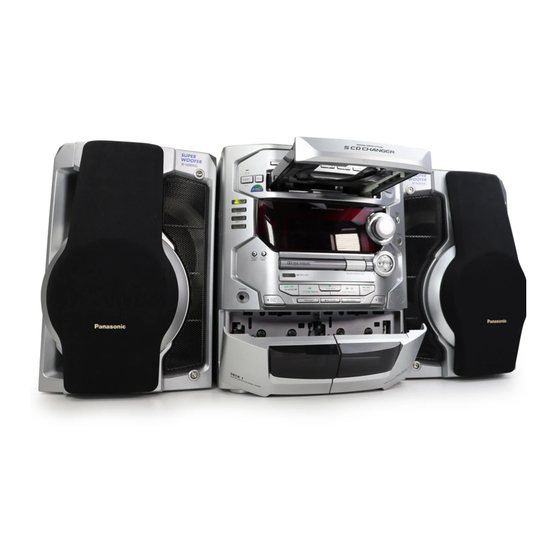
Page 7: Location Of Controls
6. Location of Controls... -
Page 8: Location Of Controls For Remote Control Transmitter
7. Location of Controls for Remote Control Transmitter... -
Page 9: Operation Checks And Component Replacement Procedures
8. Operation Checks and Component Replacement Procedures - This section describes procedures for checking the operation of the major printed circuit boards and replacing the main components. - For reassembly after operation checks or replacement, reverse the respective procedures. Special reassembly procedures are described only when required. - Page 10 8.1. Checking for the main P.C.B.
- Page 11 - Check the main P.C.B. as shown below. 8.2. Disassembly for the CD changer ass’y (The CD changer unit can be removed until the tray base / ornament would removed.) 8.2.1. Disassembly for the disc tray ornament - Follow the (Step 1) - (Step 3) of item 8.1.
- Page 14 8.2.2. Disassembly for the CD changer unit - Follow the (Step 1) - (Step 3) of item 8.1. - Follow the disassembly instruction for the disc tray / ornament of item 8.2.1.
- Page 15 8.3. Checking for the unit operational condition (Place the unit horizontally when loading the CD changer unit.) 8.3.1. Initial setting of CD unit - Follow the (Step 1) - (Step 3) of item 8.1. - Follow the disassembly instruction for the disc tray / ornament of item 8.2.1.
- Page 16 8.3.2. Checking for the CD servo P.C.B. - The initial setting of CD unit must be completed. / (Refer to the initial setting of CD unit in item 8.3.1.)
- Page 17 - Check the CD servo P.C.B. as shown below. 8.3.3. Checking for the dolby prologic P.C.B. FL P.C.B. and cassette mechanism control P.C.B. - The initial setting of CD unit must be completed. / (Refer to the initial setting of CD unit in item 8.3.1.)
- Page 18 - Check the dolby proloogic P.C.B. FL P.C.B. and / cassette mechanism control P.C.B. as shown below. 8.3.4. Checking for the power supply P.C.B. - The initial setting of CD unit must be completed. / (Refer to the initial setting of CD unit in item 8.3.1.)
- Page 19 - Check the power supply P.C.B. as shown below. 8.4. Replacement for the traverse deck ass’y - Follow the (Step 1) - (Step 3) of item 8.1.
- Page 20 - Follow the disassembly instruction for the disc tray / ornament of item 8.2.1. - Follow the disassembly instruction for the CD changer / unit of item 8.2.2.
- Page 24 8.5. Replacement for the disc tray - Follow the (Step 1) - (Step 3) of item 8.1. - Follow the disassembly instruction for the disc tray / ornament of item 8.2.1. - Follow the disassembly instruction for the CD changer / unit of...
- Page 25 item 8.2.2.
- Page 28 8.6. Disassembly and reassembly for mechanism base drive unit - Follow the (Step 1) - (Step 11) of item 8.1. - Follow the disassembly instruction for the disc tray / ornament of item 8.2.1. - Follow the disassembly instruction for the CD changer / unit of item 8.2.2.
- Page 38 8.7. Replacement for the motor ass’y - Follow the (Step 1) - (Step 3) of item 8.1. - Follow the disassembly instruction for the disc tray / ornament of item 8.2.1. - Follow the disassembly instruction for the CD changer / unit of item 8.2.2.
- Page 40 8.8. Replacement for the pinch roller ass’y and head block - Follow the (Step 1) - (Step 3) of item 8.1. - Follow the disassembly instruction for the disc tray / ornament of item 8.2.1. - Follow the disassembly instruction for the CD changer / unit of item 8.2.2.
- Page 42 8.9. Replacement for the CD motor ass’y, capstan belt A, capstan belt B and winding belt - Follow the (Step 1) - (Step 3) of item 8.1. - Follow the disassembly instruction for the disc tray / ornament of item 8.2.1. - Follow the disassembly instruction for the CD changer / unit of item 8.2.2.
- Page 46 8.10. Replacement for the components parts on the mechanism P.C.B. - Follow the (Step 1) - (Step 3) of item 8.1. - Follow the disassembly instruction for the disc tray / ornament of item 8.2.1. - Follow the disassembly instruction for the CD changer / unit of item 8.2.2.
- Page 47 8.12. Measure for tape trouble - Follow the (Step 1) - (Step 3) of item 8.1.
-
Page 48: Checking Procedure For Self-Operation Of Cassette Mechanism Ass'y
9. Checking Procedure for Self-operation of Cassette Mechanism Ass’y - This procedure describes simple methods independent of mechanism controller or governor circuit. 9.1. Operation Check Providing with Cassette Tape 1. Push up the EJECT lever with rubber band.(Refer to Fig. 2. - Page 49 power ON/OFF. (Power: +PL, -PL) (Refer to Fig. A. FWD PLAY : Supply power to the plunger momentary. (Duration : approx. 50msec.) B. FWD FF : At FWD PLAY mode, supply power to the plunger momentary. (Duration: approx. 50msec.) C. STOP : At FWD FF mode, supply power to the plunger momentary.
- Page 50 9.1.2. Detail View of EJECT Lever / (EJECT lever fixed by rubber band, Plunger rib operation) Fig. 2...
-
Page 51: Self-Diagnostic Display Function
9.2. Operation Check Not Provided with Cassette Tape 1. Push up the EJECT lever with rubber band. (Refer to Fig. 2. Apply DC 5V to the MOTOR. (MOTOR will be rotated) 3. Lift up the plunger rib of mechanism ass’y with the tip of minus screwdriver, and then operate it same as power supply duration. - Page 52 Cassette Mechanism Test / (For error code H01, H02, H03, F01, F02) 1. Press “TAPE, DECK 1/2” to select Deck 2. 2. Load a cassette tape with the erasure prevention tab removed from the left side only and close the cassette holder. 3.
-
Page 53: Description Of Error Code
8. Press “ REC/STOP” button. (Tape will not move) 9. Press “ TUNE MODE” button to indicate Error Code. (Error Code is displayed for DECK1 when DECK selector is switched to DECK1 and display for DECK2 when it is switched to DECK2) 10. - Page 54 Error Error Problem Condition Display 1 MODE SW detection error Faulty operation of cassette mechanism. / Faulty contact or short-circuit of mechanism mode switch (S951, S971) 2 REC INH SW detection Recording not possible. / Faulty contact or short-circuit error REC INH switch (S974, S975) 3 HALF SW detection error Playback can not perform.
-
Page 55: Cd Test Mode Function
12. CD Test Mode Function This CD test mode is provided to check CD unit without connecting to changer loading mechanism. This mode shall operate CD PLAY with CD unit being connected only and CD Automatic Alignment result is shown on FL display. How to set CD test mode CD Automatic Alignment result indication Under CD test mode, pressing the numeric key ’0’... -
Page 56: Measurement And Adjustments
13. Measurement and Adjustments 13.1. Tuner Section 13.1.1. Measuring Instruments and Special Tools - AM signal generator (AM-SG) - EVM-AC (AC Electronic voltmeter) - EVM-DC (DC Electronic voltmeter) - Osciloscope - Choke coil (100 - AM loop antenna Note: - Trimmer will be instability that once you tighten, please adjust with tighten slowly from loosened condition. - Page 57 13.1.3. AM RF Adjustment 1. Connect the instrument as shown in Fig.3. 2. Set the unit to AM mode. 3. Set AM-SG to 520kHz. 4. Receive 520kHz in the unit. 5. Adjust Z101 (OSC) so that the EVM-AC is maximized. 6.
- Page 58 13.2. Cassette Deck Section 13.2.1. Measuring Instruments and Special Tools - Digital frequency counter - EVM-AC (AC Electronic voltmeter) - Test tape / QZZCFM : Head azimuth adjustment / QZZCWAT : Tape speed adjustment / QZZCRA : Normal reference blank tape / QZZCRX : CrO2 tape 13.2.2.
- Page 59 channels does not exceed 0.5dB. 3. Perform the same adjustment in reverse playback mode. / Checking of the level difference forward and reverse directions 4. Playback the playback gain adjustment portion (315Hz, 0dB) of test tape (QZZCFM). Check if level difference between forward and reverse direction is within 1.5dB.
- Page 60 Fig.8 13.2.3. Tape Speed Adjustment (Deck 1/2) 1. Insert the test tape (QZZCWAT) to Deck 2 and playback (FWD side) the middle portion of it. 2. Adjust motor VR (Deck 2) for the output value shown below. / Adjustment target : 2940 - 3060Hz (NORMAL speed) 3.
- Page 61 13.2.4. Bias OSC Frequency Adjustment / (Deck 2) 1. Set the unit to “AUX” position. 2. Insert the Normal blank tape (QZZCRA) into DECK2 and set the unit to “REC” mode (use “ REC/STOP” key). 3. Adjust L1201 so that the output freguency is within the standard value.
- Page 62 1. Set the unit to “AUX” position. 2. Insert the Normal blank tape (QZZCRA) into DECK2 and set the unit to “REC” mode (use “ REC/STOP” key). 3. Measure and make sure that the output is within the standard value. 4.
- Page 63 : Tray position 1 detect switch in OFF position : Tray position 2 detect switch in OFF position : Tray open detect switch in OFF position : Clump switch in OFF position : Bottom switch on OFF position : CD management switch (CD MANAGER) S600 : Sound control jog switch (SOUND S600A...
- Page 64 : Sound EQ right switch ( ) S626 : Play timer/record timer switch ( PLAY/ S627 REC) : 3D AI EQ switch (3D AI EQ) S628 : Auxiliary input switch (AUX) S629 : Super woofer switch (S. WOOFER) S630 : Tape/deck select switch (TAPE/DECK 1/2) S631 : Display select/demonstration mode S632...
-
Page 65: Printed Circuit Board Diagram
When replacing any of components, be sure to use only manufacturers specified parts shown in the parts list. - Caution! / IC and LSI are sensitive to static electricity. / Secondary trouble can be prevented by taking care during repair. / Ground the soldering iron. - Page 66 Function Terminal Name CRT/ CRT timer SER4 TPS signal input 3 DECK1 Deck1 mechanism condition input 4 DECK2 Deck2 mechanism condition input KEY4- Operation switch signal input KEY1 SER1 Serial clock output for IC601 and IC602 10 CDRST Reset signal output for CD circuit 11 SER3 Serial data output for IC303 and...
- Page 67 Function Terminal Name 27 MDATA/ CD command data output and tuner PLL data output PLLDA 28 MCLK/ CD command data output and tuner PLL clock output PLLCLK 29 REST Rest switch (S701) signal input 30 BLKCK CD subcode block clock input Remote control signal input 32 DCDET DC ditect terminal...
- Page 68 Function Terminal Name FL segment signal output SEG3 / | / SEG1 95 REG IN Region select signal input 96 EEDATA Serial data output for IC801 and IC803 97 EECLK Not used, open Power supply (-30V) 99 AVSS 100 VREF Reference voltage input 20.2.
- Page 69 Function Terminal Name Tracking error signal input 23 TEOUT Tracking error signal output 24 FEOUT Focus error signal output Focus error signal input 26 VREF Reference voltage output 27 TBAL Tracking balance adj. input 28 FBAL Focus balance adj. input 20.3.
- Page 70 Function Terminal Name 19 SMCK System clock (f=4.2336 MHz) (Not used, open) 20 CSEL Frequency control terminal of crystal oscillator (Connected to Traverse servo control signal output (Not used, open) Traverse drive signal output Turntable motor drive signal output (L: ON) Turntable motor drive signal output (Forced mode)
- Page 71 Function Terminal Name RF signal input IREF Reference current input DSL bias terminal DSLF I/O DSL loop filter terminal PLLF I/O PLL loop filter terminal 49 VCOF VCO loop filter terminal (Not used, connected to GND) 50 AV Power supply terminal 51 AV GND terminal EFM signal (Not used, open)
- Page 72 Function Terminal Name 71 /TEST Test terminal (Not used, connected to power supply) 72 AV Power supply terminal 73 OUTL L ch audio signal output 74 AV GND terminal 75 OUTR R ch audio signal output 76 RSEL Polarity direction control terminal of RF signal (Not used, connected to power supply) 77 IOV...
-
Page 73: Replacement Parts List
Function Terminal Name Motor driver 4 output terminal (-) Motor driver 4 output terminal Not used 19 PGND2 Driver GND terminal 2 20 PV Driver power supply terminal 2 Power supply terminal 22 VREF Reference voltage input terminal Motor driver 4 input Motor driver 3 input 25 RSTIN Reset terminal... - Page 74 Ref. No. Part No. Part Name & Description Pcs. Remarks CABINET AND CHASSIS REEX0065 20P FFC 1 [M] REEX0081 19P FFC WIRE 1 [M] REEX0082 26P FFC 1 [M] RGP0784D-S FRONT PANEL 1 [M] RGU1847-S RANDOM BUTTON 1 [M] RGU1855-S DEMO BUTTON 1 [M] RGU1849-Q...
- Page 75 Ref. No. Part No. Part Name & Description Pcs. Remarks XTW3+15T SCREW 4 [M] XTB3+10JFZ SCREW 5 [M] XTBS3+8JFZ1 SCREW 26 [M] XTBS26+10J SCREW 20 [M] XTB3+20J SCREW 2 [M] XTW3+12T SCREW 4 [M] XTB3+10J SCREW 2 [M] RSC0027-2 TUNER PACK 1 [M] REEX0083 14P FFC WIRE...
- Page 76 Ref. No. Part No. Part Name & Description Pcs. Remarks XTW26+10S SUB-CHASSIS SCREW 6 [M] XYC2+JF17 PCB EARTH SCREW 2 [M] RFKJXED70-K CHASSIS ASS'Y 1 [M] TRAVERSE DECK RML0517 TIMING LEVER 1 [M] RML0516 PLUNGER LEVER 1 [M] RMB0551 UPPER SPINDLE SPRING 1 [M] RMQ0744 LOWER HOOK...
- Page 77 Ref. No. Part No. Part Name & Description Pcs. Remarks RME0263 CLICK SPRING 1 [M] RMQ0743 SPINDLE SHAFT 1 [M] RMB0552 CUSHION SPRING 1 [M] RDG0430 RELAY GEAR 'A' 1 [M] RDG0431 RELAY GEAR 'B' 1 [M] RME0262 DISK LEVER SP. 1 [M] RMA1105 SUPPORT PLATE...
- Page 78 Ref. No. Part No. Part Name & Description Pcs. Remarks 2SK544F-AC TRANSISTOR 1 [M] RVTDTC143EST TRANSISTOR 1 [M] 2SC2786MTA TRANSISTOR 1 [M] 2SC2787FL1TA TRANSISTOR 1 [M] 2SC2787FL1TA TRANSISTOR 1 [M] Q101 2SC2058SPTA TRANSISTOR 1 [M] Q106 KRA102MTA TRANSISTOR 1 [M] Q200 KTD1304TA TRANSISTOR...
- Page 79 Ref. No. Part No. Part Name & Description Pcs. Remarks Q1120 2SC2412KT96R TRANSISTOR 1 [M] Q1121 2SC2412KT96R TRANSISTOR 1 [M] Q1151 DTC144TKA146 TRANSISTOR 1 [M] Q1152 DTC144TKA146 TRANSISTOR 1 [M] Q1153 2SC2412KT96R TRANSISTOR 1 [M] Q1154 2SC2412KT96R TRANSISTOR 1 [M] Q1171 2SD1302STA TRANSISTOR...
- Page 80 Ref. No. Part No. Part Name & Description Pcs. Remarks D516 1D3E DIODE 1 [M] D517 RK306LFU1 DIODE 1 [M] D518 RVD1SS133TA DIODE 1 [M] D519 RK306LFU1 DIODE 1 [M] D520 1D3E DIODE 1 [M] D521 1D3E DIODE 1 [M] D522 MTZJ15CTA DIODE...
- Page 81 Ref. No. Part No. Part Name & Description Pcs. Remarks D985 1D3E DIODE 1 [M] D986 1D3E DIODE 1 [M] D1171 MA111TX DIODE 1 [M] D1172 MA8047MTX DIODE 1 [M] D1173 MA111TX DIODE 1 [M] D1174 MA8036HTX DIODE 1 [M] D1175 MA111TX DIODE...
- Page 82 S638 EVQ21405R SW POWER 1 [M]...
- Page 83 Ref. No. Part No. Part Name & Description Pcs. Remarks S701 RSH1A043-U SW REST 1 [M] S951 RSH1A018-3U SW LEAF 1 [M] S952 RSH1A019-2U SW LEAF 1 [M] S953 RSH1A019-2U SW LEAF 1 [M] S971 RSH1A018-3U SW LEAF 1 [M] S972 RSH1A019-2U SW LEAF...
- Page 84 Ref. No. Part No. Part Name & Description Pcs. Remarks RLQZP1R2KT-Y COIL 1 [M] RLQZPR47KT-Y COIL 1 [M] L102 RLQB1R0KTD-D INDUCTOR 1 [M] L602 RLQZP101KT-Y AXIAL COIL 1 [M] L603 RLQZP101KT-Y AXIAL COIL 1 [M] L604 RLQZP100KT-Y AXIAL COIL 1 [M] L605 RLQZP3R3KT-Y AXIAL COIL...
- Page 85 Ref. No. Part No. Part Name & Description Pcs. Remarks EYF52BC FUSE HOLDER 1 [M] EYF52BC FUSE HOLDER 1 [M] HOLDERS H501 RJS1A5513 13P WIRE HOLDER 1 [M] H600 RMR0317 8P CABLE HOLDER 1 [M] H601 RMR0317 8P CABLE HOLDER 1 [M] H602 RMR0317...
- Page 86 RSA0006-J FM ANTENNA 1 [M]...
- Page 87 Ref. No. Part No. Part Name & Description Pcs. Remarks RSA0029 AM LOOP ANTENNA 1 [M] RESISTORS ERDS2TJ102T 1K 1/4W 1 [M] ERDS2TJ104T 100K 1/4W 1 [M] ERDS2TJ104T 100K 1/4W 1 [M] ERDS2TJ221T 220 1/4W 1 [M] ERDS2TJ104T 100K 1/4W 1 [M] ERDS2TJ564T 560K 1/4W...
- Page 88 Ref. No. Part No. Part Name & Description Pcs. Remarks R145 ERJ6GEYJ104V 100K 1/10W 1 [M] R146 ERJ6GEYJ104V 100K 1/10W 1 [M] R151 ERJ6GEYJ820V 82 1/10W 1 [M] R152 ERJ6GEY0R00V 0 1/10W 1 [M] R201 ERJ6GEYJ103V 10K 1/10W 1 [M] R202 ERJ6GEYJ472V 4.7K 1/10W...
- Page 89 Ref. No. Part No. Part Name & Description Pcs. Remarks R327 ERJ6GEYJ154V 150K 1/10W 1 [M] R332 ERJ6GEYJ824V 820K 1/10W 1 [M] R334 ERJ6GEYJ274V 270K 1/10W 1 [M] R335 ERJ6GEYJ472V 4.7K 1/10W 1 [M] R336 ERJ6GEYJ153V 15K 1/10W 1 [M] R337 ERJ6GEYJ822V 8.2K 1/10W...
- Page 90 Ref. No. Part No. Part Name & Description Pcs. Remarks R440 ERJ6GEYJ473V 47K 1/10W 1 [M] R444 ERJ6GEYJ223V 22K 1/10W 1 [M] R448 ERJ6GEYJ390V 39 1/10W 1 [M] R449 ERJ6GEYJ390V 39 1/10W 1 [M] R452 ERJ6GEYJ103V 10K 1/10W 1 [M] R453 ERJ6GEYJ472V 4.7K 1/10W...
- Page 91 Ref. No. Part No. Part Name & Description Pcs. Remarks R574 ERDS1FVJ272T 2.7K 1/2W 1 [M] R575 ERDS1FVJ470T 47 1/2W 1 [M] R576 ERDS1FVJ470T 47 1/2W 1 [M] R577 ERDS1FVJ2R2T 2.2 1/2W 1 [M] R578 ERDS2TJ332T 3.3K 1/4W 1 [M] R583 ERDS1FVJ100T 10 1/2W...
- Page 92 Ref. No. Part No. Part Name & Description Pcs. Remarks R643 ERDS2TJ392T 3.9K 1/4W 1 [M] R648 ERDS2TJ272T 2.7K 1/4W 1 [M] R650 ERDS2TJ472T 4.7K 1/4W 1 [M] R651 ERDS2TJ222T 2.2K 1/4W 1 [M] R652 ERDS2TJ272T 2.7K 1/4W 1 [M] R653 ERDS2TJ222T 2.2K 1/4W...
- Page 93 Ref. No. Part No. Part Name & Description Pcs. Remarks R714 ERJ6GEY0R00A 0 1/10W 1 [M] R715 ERJ6GEYJ102A 1K 1/10W 1 [M] R717 ERJ6GEYJ102A 1K 1/10W 1 [M] R718 ERJ6GEYJ102A 1K 1/10W 1 [M] R721 ERJ6GEYJ101A 100 1/10W 1 [M] R723 ERJ6GEYJ682A 6.8K 1/10W 1 [M]...
- Page 94 Ref. No. Part No. Part Name & Description Pcs. Remarks R877 ERJ6GEYJ223V 22K 1/10W 1 [M] R878 ERJ6GEYJ102V 1K 1/10W 1 [M] R879 ERJ6GEYJ223V 22K 1/10W 1 [M] R880 ERJ6GEYJ102V 1K 1/10W 1 [M] R890 ERJ6GEYJ561V 560 1/10W 1 [M] R892 ERJ6GEYJ393V 39K 1/10W...
- Page 95 Ref. No. Part No. Part Name & Description Pcs. Remarks R963 ERDS2TJ103T 10K 1/4W 1 [M] R964 ERDS2TJ223T 22K 1/4W 1 [M] R965 ERDS2TJ103T 10K 1/4W 1 [M] R966 ERDS2TJ472T 4.7K 1/4W 1 [M] R967 ERDS2TJ223T 22K 1/4W 1 [M] R968 ERDS2TJ101T 100 1/4W...
- Page 96 Ref. No. Part No. Part Name & Description Pcs. Remarks R1126 ERJ6GEYJ102A 1K 1/10W 1 [M] R1131 ERJ6GEYJ683A 68K 1/10W 1 [M] R1132 ERJ6GEYJ335A 3.3M 1/10W 1 [M] R1133 ERJ6GEYJ332A 3.3K 1/10W 1 [M] R1134 ERJ6GEYJ474A 470K 1/10W 1 [M] R1139 ERJ6GEYJ103A 10K 1/10W 1 [M]...
- Page 97 Ref. No. Part No. Part Name & Description Pcs. Remarks R1227 ERJ6GEYJ102A 1K 1/10W 1 [M] R1230 ERJ6GEYJ472A 4.7K 1/10W 1 [M] R1232 ERJ6GEYJ102A 1K 1/10W 1 [M] R1233 ERJ6GEYJ222A 2.2K 1/10W 1 [M] R1234 ERJ6GEYJ472A 4.7K 1/10W 1 [M] R1235 ERJ6GEYJ472A 4.7K 1/10W 1 [M]...
- Page 98 Ref. No. Part No. Part Name & Description Pcs. Remarks C134 ECUV1H270JCN 27P 50V 1 [M] C136 ECUV1H102KBN 1000P 50V 1 [M] C137 ECUV1H332KBN 3300P 50V 1 [M] C138 ECUV1H103KBN 0.01 50V 1 [M] C139 ECEA1EKA4R7B 4.7 25V 1 [M] C141 ECEA1HKA010B 1 50V 1 [M]...
- Page 99 Ref. No. Part No. Part Name & Description Pcs. Remarks C308 ECUZ1E473ZFN 0.047 25V 1 [M] C312 ECUZ1E104ZFN 0.1 25V 1 [M] C313 ECUZ1E104ZFN 0.1 25V 1 [M] C314 ECUV1H151KCN 150P 50V 1 [M] C315 ECUV1H151KCN 150P 50V 1 [M] C316 ECUV1H151KCN 150P 50V 1 [M]...
- Page 100 Ref. No. Part No. Part Name & Description Pcs. Remarks C435 ECUZ1E183KBN 0.018 25V 1 [M] C436 ECUZ1H101JCN 100P 50V 1 [M] C437 ECUZ1H102KBN 1000P 50V 1 [M] C440 ECEA1HKA010B 1 50V 1 [M] C441 ECUZ1H101JCN 100P 50V 1 [M] C442 ECEA1HKA3R3B 3.3 50V 1 [M]...
- Page 101 C570 ECBT1H104ZF5 0.1 50V 1 [M] Ref. No. Part No. Part Name & Description Pcs. Remarks C571 RCE1VFW332BJ 3300 35V 1 [M] C572 RCE1VFW562BJ 5600 35V 1 [M] C573 RCE1VFW562BJ 5600 35V 1 [M] C574 RCE1VFW332BJ 3300 35V 1 [M] C575 ECEA1HKA101B 100 50V 1 [M]...
- Page 102 Ref. No. Part No. Part Name & Description Pcs. Remarks C654 ECBT1E103ZF5 0.01 25V 1 [M] C655 ECBT1H150JC5 15P 50V 1 [M] C656 ECBT1H101KB5 100P 50V 1 [M] C657 ECBT1H180JC5 18P 50V 1 [M] C658 ECBT1H101KB5 100P 50V 1 [M] C659 ECBT1H680J5 68P 50V...
- Page 103 Ref. No. Part No. Part Name & Description Pcs. Remarks C743 ECUZ1E104ZFN 0.1 25V 1 [M] C744 ECUZ1E822KBN 8200P 25V 1 [M] C745 ECUZ1H102KBN 1000P 50V 1 [M] C747 ECUZ1H181KCN 180P 50V 1 [M] C749 ECUZ1H222KBN 2200P 50V 1 [M] C750 ECUZ1E104MBN 0.1 25V 1 [M]...
- Page 104 Ref. No. Part No. Part Name & Description Pcs. Remarks C848 ECEA1HKAR15B 0.15 50V 1 [M] C851 ECEA1CM221B 220 16V 1 [M] C861 ECEA1HKA2R2B 2.2 50V 1 [M] C862 ECEA1HKA2R2B 2.2 50V 1 [M] C863 ECEA1HKA0R1B 0.1 50V 1 [M] C864 ECKR1H473ZF5 0.047 50V 1 [M]...
- Page 105 Ref. No. Part No. Part Name & Description Pcs. Remarks C1128 ECUZ1H103KBN 0.01 50V 1 [M] C1129 ECUZ1H821KBN 820P 50V 1 [M] C1130 ECUZ1H821KBN 820P 50V 1 [M] C1131 ECUZ1H821KBN 820P 50V 1 [M] C1132 ECUZ1H821KBN 820P 50V 1 [M] C1133 ECEA1HKA4R7B 4.7 50V 1 [M]...
-
Page 106: Cabinet Parts Location
Ref. No. Part No. Part Name & Description Pcs. Remarks RJ708 ERJ8GEY0R00A 0 1/8W 1 [M] RJ709 ERJ8GEY0R00A 0 1/8W 1 [M] RJ710 ERJ8GEY0R00A 0 1/8W 1 [M] RJ712 ERJ8GEY0R00A 0 1/8W 1 [M] RJ715 ERJ6GEY0R00A 0 1/10W 1 [M] RJ716 ERJ6GEY0R00A 0 1/10W 1 [M]... -
Page 108: Mechanism Parts Location
23. Mechanism Parts Location... -
Page 110: Cd Mechanism Parts Location
24. CD Mechanism Parts Location... - Page 111 25. Packaging...
- Page 112 Printed in Japan (M000500000MT)
-
Page 113: Electrical Parts Location
ELECTRICAL PARTS LOCATION Ref. No. Lo. No. Ref. No. Lo. No. Ref. No. Lo. No. Ref. No. Lo. No. Ref. No. Lo. No. Ref. No. Lo. No. Ref. No. Lo. No. Ref. No. Lo. No. MECHANISM P.C.B. (DECK 1) IC951 S951 CS951 S952... - Page 114 OPERATION ( 1 ) P.C.B. OPERATION ( 2 ) P.C.B. 1 2 3 4 5 6 7 8 H600/W600 S612 DECK 1 OPEN) ELECTRICAL PARTS LOCATION S600 (CD MANAGER) Ref. No. Lo. No. Ref. No. Lo. No. S621 OPERATION (2) P.C.B. FM MODE/BP) D605 R618...
- Page 115 POWER AMP P.C.B. D503 C534 H501/W501 D502 D507 D509 ELECTRICAL PARTS LOCATION R565 Ref. Ref. Ref. Q519 C550 Q516 D516 D518 B C E POWER AMP P.C.B. R551 Q501 IC500 R517 C503 R598 R569 RL501 R529 IC501 R520 C508 C546 B C E Q501 R521...
- Page 116 DPL P.C.B. R843 C832 C866 C816 C829 C818 C851 C820 C833 C837 C830 C889 C861 R857 R871 C831 C817 R836 R867 R890R866 C821 C899 R807 C823 C811 R822 R823 C810 C819 1 2 3 R880 R805 R868 X801 C883 R878 C828 C897 C874...
-
Page 117: Loading Motor P.c.b
POWER TRANSFORMER P.C.B. LOADING MOTOR P.C.B. Q977 CN502 E C B R984 C981 C980 R985 R983 R981 (LOADING MOTOR) Q978 D981 D978 CN501 D977 D986 W500 D513 E C B Q975 RL502 C540 T501(POWER TRANSFORMER) PLUNGER (REP2578A-N) ELECTRICAL PARTS LOCATION Ref. -
Page 118: Schematic Diagram
SCHEMATIC DIAGRAM-1 NOTE: The number which noted at the connectors on the schematic diagram as "SCHEMATIC DIAGRAM-1" or "SCHEMATIC DIAGRAM-2" indicates the schematic diagram serial number located on the left corner in the schematic diagram. CD SERVO CIRCUIT :POSITIVE VOLTAGE LINE :CD SIGNAL LINE 3.2V OPTICAL PICKUP... - Page 119 SCHEMATIC DIAGRAM-2 :POSITIVE VOLTAGE LINE :CD SIGNAL LINE 3.2V 3.2V TP18 TP20 TP23 R717 C727 50V1 PLAY C731 6.3V220 2.2V 1kHz, 0dB C730 TP21 R718 C728 50V1 3.2V 2.1V 62 63 64 65 66 67 68 69 70 71 72 73 74 75 76 77 78 79 80 F=16.9344MHz 3.2V BCLK...
- Page 120 SCHEMATIC DIAGRAM-3 :FM SIGNAL LINE :AM SIGNAL LINE MAIN(TUNER) CIRCUIT :POSITIVE VOLTAGE LINE :FM OSC SIGNAL LINE :AM OSC SIGNAL LINE FM FRONT END(Z120) CIRCUIT 2SC2786MTA FM MIXER 2SK544F-AC 0.47 2.2P RF AMP 5.6P JK101 FM ANT R103 100K 680K 680K 4.7P 3.3P...
- Page 121 SCHEMATIC DIAGRAM-4 :POSITIVE VOLTAGE LINE :FM SIGNAL LINE :AM SIGNAL LINE :AM OSC SIGNAL LINE R104 R107 R106 CF202 470K CF201 C104 10.3V Q106 1000P 0.7V KRA102MTA POWER SUPPLY Q101 (FM:ON) 2SC2058SPTA LINE FM IF AMP 14.5V 14.3V 14.5V 14.5V 14.5V 14.4V IC101...
- Page 122 SCHEMATIC DIAGRAM-5 :TAPE PLAYBACK SIGNAL LINE MECHANISM CONTROL CIRCUIT :POSITIVE VOLTAGE LINE :TAPE RECORDING SIGNAL LINE 14.5V R1103 C1193 C1101 1000P 1000P R1102 Q1101 ((0V)) 100K ((4.2V)) 2SJ498CDTA DECK1 HEAD SELECT ((0V)) (REC:ON) L ch CS1101 PLAYBACK HEAD Q1103 ((0V)) ((4.4V)) 2SJ498CDTA R ch...
- Page 123 SCHEMATIC DIAGRAM-6 :TAPE PLAYBACK SIGNAL LINE :POSITIVE VOLTAGE LINE :TAPE RECORDING SIGNAL LINE 14.5V C1133 50V4.7 Q1107 DTC144TKA146 P.B EQ/ REC EQ (CrO / H.SPEED) R1121 ((4.8V)):CrO ((0V)) ((0V)) C1129 C1131 C1135 C1146 820P 820P 1000P 16V10 R1115 R1146 390K C1115 R1109 C1127...
- Page 124 SCHEMATIC DIAGRAM-7 :TAPE PLAYBACK SIGNAL LINE MECHANISM CONTROL CIRCUIT :POSITIVE VOLTAGE LINE : TAPE RECORDING SIGNAL LINE 14.5V Q1151,1152 DTC144TKA146 R1151 C1165 SWITCHING(PLAY:ON) 16V10 ((8.8V)) ((2.6V)) 0.1V Q1153 ((0V)) ((3.8V)) Q1151 ((2.1V)) Q1153,1154 2SC2412KT96R MUTING 0.1V ((3.8V)) Q1152 ((2.1V)) ((2.6V)) Q1154 ((0V)) ((8.8V))
- Page 125 SCHEMATIC DIAGRAM-8 :TAPE PLAYBACK SIGNAL LINE :POSITIVE VOLTAGE LINE : TAPE RECORDING SIGNAL LINE 14.5V H1100 M.GND MO.GND MO+B MAIN D.GND (CONTROL) CIRCUIT R1144 +B(14V) (CN304) Rch IN on SCHEMATIC Lch IN DIAGRAM-15 R1143 A.GND Rch OUT Z1101 Lch OUT TP10 CN1201 SW5V...
- Page 126 SCHEMATIC DIAGRAM-9 :POSITIVE VOLTAGE LINE :CENTER SP. DRIVE SIGNAL LINE DPL CIRCUIT :NEGATIVE VOLTAGE LINE :CD SIGNAL LINE :SURROUND SP. DRIVE SIGNAL LINE C851 16V220 C829 16V220 C861 50V2.2 C830 16V10 IC802 C831 16V10 BA178M09T C832 16V10 REGULATOR C833 16V10 C834 OUT GND 9.1V...
- Page 127 SCHEMATIC DIAGRAM-10 OPERATION(1) CIRCUIT :POSITIVE VOLTAGE LINE :CD SIGNAL LINE D600-604 SLR325MCT31W R616 R615 R614 R613 R612 R611 R610 R609 R608 R607 R606 6.8K 4.7K 2.7K 2.2K 1.8K 1.2K H600 (CD DIRECT PLAY/ OPEN) OPERATION(2) CIRCUIT S600A (SOUND CONTROL JOG) R629 R626 R625...
- Page 128 SCHEMATIC DIAGRAM-11 :POSITIVE VOLTAGE LINE :CD SIGNAL LINE R694 4.7K R653 2.2K R635 R650 4.7K 3.3V H601 R633 ((3.3V)) 3.3V 3.3V Z600 RCDRPM6937H4 (0V) (REMOTE SENSOR) 0.1V 4.4V IC601 BU2090AF-E2 LED DRIVE C620 C621 D607 0.01 25V4.7 SLI325URCT31 R643 (AC IN) 3.9K 0.2V 4.7V...
- Page 129 SCHEMATIC DIAGRAM-12 FL CIRCUIT :POSITIVE VOLTAGE LINE :NEGATIVE VOLTAGE LINE -28.5V L605 3.3 H C629 330P R901 R949 C645 16V10 84 83 82 81 D636 R919 RVD1SS133TA -22.1V CRT/SER4 SEG14 5.2V -22V SEG15 3.7V -28.6V DECK1 SEG16 -24.2V DECK2 SEG17 R905 5.3V -19.9V...
- Page 130 SCHEMATIC DIAGRAM-13 :POSITIVE VOLTAGE LINE :NEGATIVE VOLTAGE LINE :CD SIGNAL LINE -28.5V FL600(RSL0296-F) D638 L606 MA4020LTA FL DISPLAY 6 7 8 9 10 11 12 13 14 15 16 17 18 19 20 21 22 23 24 25 26 27 28 29 30 31 32 33 34 35 36 37 38 39 40 41 42 43 44 45 46 47 48 49...
- Page 131 SCHEMATIC DIAGRAM-14 :POSITIVE VOLTAGE LINE LOADING MOTOR CIRCUIT TA7291P MOTOR DRIVE CLAMP SW 0.6V 9.7V 9.8V 9.8V 0.6V CIRCUIT 0.01 (CLAMP) PLUNGER (LOADING MOTOR) (TRAY POSITION2 DET.) (TRAY POSITION1 DET.) BOTTOM SW CIRCUIT (OPEN DET.) (BOTTOM) 7.7V 8.7V RVTDTC143EST A B C D MOTOR DRIVE GP1S94 (POSITION SENSOR)
-
Page 132: Main(Control) Circuit
SCHEMATIC DIAGRAM-15 :POSITIVE VOLTAGE LINE :CD SIGNAL LINE :FM SIGNAL LINE :CENTER SP. DRIVE SIGNAL LINE :TAPE PLAYBACK SIGNAL LINE :AM SIGNAL LINE :SURROUND SP. DRIVE SIGNAL LINE :TAPE RECORDING SIGNAL LINE :NEGATIVE VOLTAGE LINE FL CIRCUIT(CP603) on SCHEMATIC DIAGRAM-13 MAIN(CONTROL) CIRCUIT R401 JK305... - Page 133 SCHEMATIC DIAGRAM-16 :CD SIGNAL LINE :TAPE PLAYBACK SIGNAL LINE :POSITIVE VOLTAGE LINE :FM SIGNAL LINE :NEGATIVE VOLTAGE LINE :AM SIGNAL LINE :TAPE RECORDING SIGNAL LINE FL CIRCUIT(CP602) on SCHEMATIC DIAGRAM-13 IC302 C228 R225 R224 R248 R249 16V10 3.6K M5218AP 18 19 24 25 BUFFER AMP C229...
- Page 134 SCHEMATIC DIAGRAM-17 :CD SIGNAL LINE :POSITIVE VOLTAGE LINE :CENTER SP. DRIVE SIGNAL LINE MAIN(CONTROL) CIRCUIT :NEGATIVE VOLTAGE LINE :SURROUND SP. DRIVE SIGNAL LINE R434 C440 2.2K 50V1 IC301 M62456FPE1 C322 R336 R337 0.068 8.2K BTL BASS BOOST C435 R431 0.018 R444 C441 100P...
- Page 135 SCHEMATIC DIAGRAM-18 :NEGATIVE VOLTAGE LINE :CENTER SP. DRIVE SIGNAL LINE POWER AMP CIRCUIT :POSITIVE VOLTAGE LINE :CD SIGNAL LINE :SURROUND SP. DRIVE SIGNAL LINE IC500 RSN311W64A-P POWER AMP(HIGH,MID,LOW) -58V -28V -0.2V 0.2V -28V -58V R552 -28V R553 -58V R502 4.7K C500 470P R505...
- Page 136 SCHEMATIC DIAGRAM-19 :NEGATIVE VOLTAGE LINE :CENTER SP. DRIVE SIGNAL LINE :POSITIVE VOLTAGE LINE :CD SIGNAL LINE :SURROUND SP. DRIVE SIGNAL LINE IC501 STK470-040 REGULATOR JK502 9.8V 4.9V -27V -8.4V -7.5V 7.5V 14.7V 16V -29V -58V C544 C552 0.01 0.01 SPEAKERS (6 ) R590 R599...
- Page 137 SCHEMATIC DIAGRAM-20 POWER TORANSFORMER CIRCUIT Q978 KRC102MTA SWITCHING R976 -0.3V :POSITIVE VOLTAGE LINE :NEGATIVE VOLTAGE LINE D978 D981 D979 R980 R981 R985 1D3E 1D3E 1D3E AC IN CIRCUIT Q977 2SC3940AQSTA REGULATOR C978 0.01 W500 9.5V 6.6V T502 R984 CN502 SYNC FL CIRCUIT (H603) on R978...
- Page 138 MN662790RSC M5218AP BA7755A AN8839NSBE2 28PIN BU2090AF-E2 16PIN LA1833NMNTLM 24PIN ..... . LC72131MDTRM 20PIN No.1 M51167AFP-TB 36PIN ..
- Page 139 AC IN P.C.B. AC IN [DECK 2] [DECK 1] PLAYBACK R/P HEAD, HEAD ERASE HEAD T502 (POWER TRANSFORMER) 1 . . . 5 1 . . . 5 W500 CN502 1 . 3 1 . 5 1 . 5 CS1102 CS1101 H1100 CN501...
-
Page 140: Operation
SPEAKERS AM ANT FM ANT MAIN P.C.B. CP501 CN300 CN801 CP304 POWER AMP P.C.B. FM FRONT END(Z120) P.C.B. P.C.B. (SOLDER SIDE) CP500 CN301 CN802 CP305 CN309 13 ... 1 CN303 CN302 CN304 2 . - Page 143 CD CHANGER SECTION AN8839NSBE2 (RF) IC701 CD OPTICAL PICKUP TJ701 SERVO AMP SEMICONDUCTOR RFIN CSBRT LASER OFTR RFENV TENV DET. Q701 Vref. LASER OFTR POWER Vref. DRIVE DET. Vref. /RFDET /RFDET DET. FE IN A ch Vref. SUBTRACTER VCBA FE OUT LDON PHOTO DETECTOR Vref.
- Page 144 : CD SIGNAL LINE NOTE MCLK MCLK MDATA MDATA STAT STAT (To MAIN SECTION) SUBQ SUBQ MN662790RSC SQCK IC702 SQCK SERVO PROCESSOR / DIGITAL SIGNAL PROCESSOR BLKCK DIGITAL FILTER / D/A CONVERTER BLKCK RESTSW S701 (REST) 79 80 IOSEL OUTR BLKCK BLKCK R ch...
-
Page 145: Main Section
MAIN SECTION FM ANT AM ANT (FM FRONT END) Z101 Q1A,D1A CF201 RF AMP FM MIXER COIL COIL Q3,D3 BUFFER FM IF LOCAL Q101 LA1833NMNTLM CF202 IC101 +B(FM) FM / AM I F AMP, DET / AM OSC, MIX / FM MPX DECODER BUFF. -
Page 146: System Control
M51167AFP-TB TP9( TP10 Q1153(Q1154) IC1101 (1/2) P.B. EQ / TPS AMP BUFFER [ DECK 1 ] 36(1) PLAYBACK HEAD 33(4) 30(7) (L ch) 32(5) TP3( Q1103 (Q1104) [ DECK 2 ] 31(6) HEAD SELECT (PLAY:ON) HEAD Q1115 (L ch) (Q1116) Q1101(Q1102) MUTING HEAD SELECT... - Page 147 (67) (59) (68) (To CD CHANGER SECTION) (69) CD signal (71) (70) (57) (66) Q304 Microcomputer SWITCH- Graphic interface equalizer M62433AFP 9~20 (63) (62) (45~56) (44) (60) (58) IC303 (37) (38) (39) (41) (42) (43) DIGITAL SOUND CONTROLLER FILTER Q400 MUTING (Q200) Q306...
- Page 148 X801 BA178M09T (8MHz) IC802 REGULATOR 29,58 8,26 BA4558FE2 IC804 BUFFER S OP OUT Q802 LV1041M MUTING IC801 (21) L MIX OUT DOLBY PRO LOGIC Q804 (R MIX OUT) CONTROL BA4558FE2 MUTING IC804 CONT. BUFFER C OP OUT Q801 MUTING L IN (R IN) Q803 50,54...
-
Page 149: Led Drive
M5218AP IC302 BUFFER CR NETWORK 19 22 R ch M62456FPE1 IC301 BTL BASS BOOST +B10 +B10 +B10 SYS6V D605 D600~603, (DOLBY D600~604,606 +B11 (TAPE,CD, (REC/PLAY, D607 LOGIC) TUNER,S.WOOFER, CD1~5) (AC IN) AUX) 10~15 9~13 REC/PLAY, SW,AUX,TAPE, G1~5 TUNER,CD BU2090AF-E2 BU2090AF-E2 IC601 IC602 LED DRIVE... -
Page 150: Power Amp
HEADPHONES RSN311W64A-P R ch IC500 POWER AMP Q510 D519 POWER CONTROL CIRCUIT SWITCH- (22) (19) SPEAKERS (11) (6 ) HIGH L ch SURROUND SPEAKERS R ch (8 ) CENTER SPEAKER (8 ) POWER CONTROL/ PROTECTION CIRCUIT Q503,505 OVER LOAD DET. D517 +/-B1 +B4 Q307,311,352... - Page 151 STK470-040 IC501 REGULATOR D526 T501 D520 AC IN D521 D503 REGULATOR LED9V D501,502 Q515 RL501 Z501 D314 Q519 POWER RL502 SUPPLY D513 Q509 POWER SWITCH- Q516, SUPPLY D512,518 CONT. ACIN FL DISPLAY Q501, (FL600) D504,514,516 REGULATOR Q975 ECONO RELAY DRIVE Q978 SYNC SWITCH-...
-
Page 152: Electrical Parts Location
Notes: This printed circuit board diagram may be modified at any time with the development of new technology. L10~12 are printed coils formed on the P.C.B. and thus not found in the replacement parts list. CD SERVO P.C.B. (RF) TJ701 ELECTRICAL PARTS LOCATION TP20 X701... - Page 153 MECHANISM CONTROL P.C.B. ELECTRICAL PARTS LOCATION Ref. Ref. Ref. Q1171 Q1173 Q1174 D1172 D1175 Q1179 R1174 MECHANISM CONTROL P.C.B. R1177 C1174 C1182 L1201 IC1101 R1126 C1104 IC1102 R1131 C1105 Q1175 IC1105 R1132 C1106 Q1101 R1133 C1108 Q1176 C1175 1 2 3 4 5 C1180 R1188 Q1102...
- Page 154 MAIN P.C.B. AM ANT FM ANT (LOOP) (EXT) (GND) JK305 JK101 C107 R112 Z101 Z120 CN300 R232 R234 D401 Q106 Q101 R334 C441 R103 R104 E C B C326 R430 R431 C327 R444 R212 C102 C204 C383 C436 R208 C125 R342 R440 CP304...
- Page 155 FM FRONT END P.C.B. Ca A B C E Ca A Ca A B C E B C E (REP1998B) ELECTRICAL PARTS LOCATION Ref. No. Lo. No. Ref. No. Lo. No. Ref. No. Lo. No. Ref. No. Lo. No. Ref. No. Lo.
- Page 156 FL P.C.B. S632 ( DISPLAY/ FL600 DEMO) 202122232425 26272829 303132333435 36 37 3839 40 41424344 4546474849 1 2 3 5 6 7 8 9 101112 13 14 16171819 5152 VR600 Q604 (VOLUME) L606 Q608 C661 D628 R961 B C E 1 2 3 R939 C659...
- Page 157 ELECTRICAL PARTS LOCATION Ref. No. Lo. No. Ref. No. Lo. No. Ref. No. Lo. No. Ref. No. Lo. No. FL P.C.B. IC600 S636 R905 C603 R643 IC601 S638 R906 C604 IC602 CN600 R907 C605 IC603 CP601 R909 C606 H601/W601 Q602 CP602 R910 C607...