Table of Contents
Advertisement
Quick Links
Advertisement
Table of Contents

Related Manuals for Aiwa XR-M78EZ

Summary of Contents for Aiwa XR-M78EZ
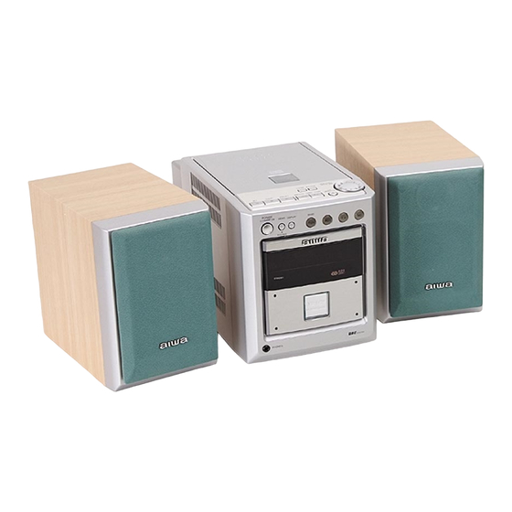
- Page 1 All manuals and user guides at all-guides.com XR-M78 XR-M77 SERVICE MANUAL COMPACT DISC STEREO BASIC CD MECHANISM : KSM-213CDM SYSTEM This Service Manual is the "Revision Publishing" and replaces "Simple Manual" (S/M Code No. 09-995-331-7T2). S/M Code No. 09-995-331-7R2...
-
Page 2: Table Of Contents
All manuals and user guides at all-guides.com TABLE OF CONTENTS SPECIFICATIONS ........................3 ACCESSORIES/PACKAGE LIST ....................3 PROTECTION OF EYES FROM LASER BEAM DURING SERVICING/ Precaution to replace Optical block .................... 4 ELECTRICAL MAIN PARTS LIST ..................5-8 TRANSISTOR ILLUSTRATION ....................9 FL GRID ASSIGNMENT/ANODE CONNECTION .............. -
Page 3: Specifications
All manuals and user guides at all-guides.com SPECIFICATIONS • Design and specifications are subject to change without notice. • Dolby noise reduction manufactured under license from Dolby Laboratories Licensing Corporation. “DOLBY” and the double-D symbol are trademarks of Dolby Laboratories Licensing Corporation. •... -
Page 4: Protection Of Eyes From Laser Beam During Servicing
All manuals and user guides at all-guides.com PROTECTION OF EYES FROM LASER BEAM DURING SERVICING This set employs laser. Therefore, be sure to follow carefully the CAUTION instructions below when servicing. Use of controls or adjustments or performance of procedures other than those specified herein may result in hazardous WARNING! radiation exposure. -
Page 5: Electrical Main Parts List
All manuals and user guides at all-guides.com ELECTRICAL MAIN PARTS LIST REF. NO PART NO. KANRI DESCRIPTION REF. NO PART NO. KANRI DESCRIPTION C552 87-010-213-080 C-CAP,S 0.015-50 B C553 87-015-688-080 CAP,E 4.7-35 7L 8Z-CL5-601-010 C-IC,LC876564 C554 87-015-688-080 CAP,E 4.7-35 7L 87-070-282-010 IC,BU2092 C555... - Page 6 All manuals and user guides at all-guides.com REF. NO PART NO. KANRI DESCRIPTION REF. NO PART NO. KANRI DESCRIPTION C213 87-012-145-080 CAP, CHIP S 270P CH C445 87-010-196-080 CHIP CAPACITOR,0.1-25 C214 87-010-178-080 CHIP CAP 1000P C446 87-010-196-080 CHIP CAPACITOR,0.1-25 C215 87-015-681-080 CAP,E 10-16 7L C447...
- Page 7 All manuals and user guides at all-guides.com REF. NO PART NO. KANRI DESCRIPTION REF. NO PART NO. KANRI DESCRIPTION CONTROL C.B C725 87-018-131-080 CAP, CER 1000P-50V C727 87-010-196-080 CHIP CAPACITOR,0.1-25 C219 87-010-197-080 CAP, CHIP 0.01 DM C728 87-010-248-080 CAP, ELECT 220-10V C220 87-010-197-080 CAP, CHIP 0.01 DM...
- Page 8 All manuals and user guides at all-guides.com REF. NO PART NO. KANRI DESCRIPTION C949 87-A10-039-080 C-CAP,U 470P-50 J CH C952 87-012-286-080 CAP, U 0.01-25 C958 87-010-197-080 CAP, CHIP 0.01 DM C959 87-010-831-080 C-CAP,U,0.1-16F C960 87-010-196-080 CHIP CAPACITOR,0.1-25 C962 87-010-401-080 CAP, ELECT 1-50V CF801 87-008-423-010 CERAMIC FILTER, SFE10.7...
-
Page 9: Transistor Illustration
All manuals and user guides at all-guides.com TRANSISTOR ILLUSTRATION FL (13-ST-36GNAK) GRID ASSIGNMENT/ANODE CONNECTION BC E 2SB1370 2SC1815 PE8050 DTC114EK 2SA933 2SA1162 PE8550 DTC114TK 2SC2712 DTC114YK DTA114YK DTA144EK... -
Page 10: Block Diagram-1
All manuals and user guides at all-guides.com BLOCK DIAGRAM-1 TUNER ADAPTOR RL881B... -
Page 11: Block Diagram-2
All manuals and user guides at all-guides.com BLOCK DIAGRAM-2... -
Page 12: Wiring-1 (Main: Inserted Parts)
All manuals and user guides at all-guides.com WIRING-1 (MAIN: INSERTED PARTS) TO/FROM TO/FROM CD C.B CN405 PT C.B WH501 MAIN C. B TUNER ADAPTOR C. B 13 14 16 16 14 EZ MODEL CN204 EZ MODEL TO/FROM FRONT C.B WH204 TO/FROM TUNER C.B CN701 TO/FROM... -
Page 13: Wiring-2 (Main: Chip Parts)
All manuals and user guides at all-guides.com WIRING-2 (MAIN: CHIP PARTS) MAIN C. B TUNER ADAPTOR C. B... -
Page 14: Schematic Diagram-1 (Main)
All manuals and user guides at all-guides.com SCHEMATIC DIAGRAM-1 (MAIN) MAIN C.B CN204 SIG/MS RD-DATA RD-CLK DGND C843 0.068 100p C844 100p PHONES 4.7/35... -
Page 15: Schematic Diagram-2 (Cd)
All manuals and user guides at all-guides.com SCHEMATIC DIAGRAM-2 (CD) CD C.B L403 100p BL01RN1 2SA933 SFR401 CURRENT LIMITER R4491 R4492 (LOADING) R4493 SWITCH SLED/ R4494 SPIN Q815-817 MOTOR (OPEN) –VF REG DRIVE Q809,810 2SC2712 (CLOSE) AC DETECT 2SC2712 2SA1162 +B SWITCH PROTECT 2SC2712... -
Page 16: Wiring-3 (Cd: Inserted Parts)
All manuals and user guides at all-guides.com WIRING-3 (CD: INSERTED PARTS) CD C. B TO/FROM MAIN C.B WH405 (OPEN) (CLOSE) (LOADING) CN404 TO/FROM FRONT C.B CN205 CONTROL C. B... -
Page 17: Wiring-4 (Cd: Chip Parts)
All manuals and user guides at all-guides.com WIRING-4 (CD: CHIP PARTS) CD C. B CONTROL C. B... -
Page 18: Wiring-5 (Front)
All manuals and user guides at all-guides.com WIRING-5 (FRONT) FRONT C.B FRONT C.B (CONDUCTOR SIDE) (COMPONENT SIDE) EZ MODEL TO/FROM CONTROL C.B WH203 TO/FROM CD C.B CN401 TO/FROM MAIN C.B CN201 WH204 TO/FROM MAIN C.B CN204 EZ MODEL... -
Page 19: Schematic Diagram-3 (Front)
All manuals and user guides at all-guides.com SCHEMATIC DIAGRAM-3 (FRONT) FRONT C.B D202,205 : IN4148 EZ MODEL LED DRIVER DRIVER SW DECODER EZ MODEL WH204 R2209 1k SIG/MS R2204 1k RD-DATA SYSTEM R2205 1k RD-CLK 2.2/50 BUFFER 0.47/ LED DRIVER RECIVER MODEL MODEL... -
Page 20: Wiring-6 (Tuner)
All manuals and user guides at all-guides.com WIRING-6 (TUNER) TO/FROM TUNER ADAPTOR C.B WH102... -
Page 21: Schematic Diagram-4 (Tuner)
All manuals and user guides at all-guides.com SCHEMATIC DIAGRAM-4 (TUNER) BALANCE BAND SW IF AMP AM IF – ANTENNA – CN701 FM/AM IF/STEREO TUNER SYSTEM TUNER ON/OFF AM TRACKING ADJ. TUNER C.B SIGNAL... -
Page 22: Wiring-7 (Pt: Inserted Parts)
All manuals and user guides at all-guides.com WIRING-7 (PT: INSERTED PARTS) PT C. B TO/FROM MAIN C. B J502 CN501 MD IN AUX IN LINE OUT TO/FROM MAIN C. B CN803 DIGITAL OUT C. B PT882 TO/FROM CD C. B CN404 LED902 DIGITAL... -
Page 23: Wiring-8 (Pt: Chip Parts)
All manuals and user guides at all-guides.com WIRING-8 (PT: CHIP PARTS) PT C. B DIGITAL OUT C. B 230V 50Hz... -
Page 24: Schematic Diagram-5 (Pt)
All manuals and user guides at all-guides.com SCHEMATIC DIAGRAM-5 (PT) PT C.B LINE MUTE DRIVE MUTE MUTE DRIVE MUTE L501 BL01RN1 MUTE DTA114YK POWER OFF DISCHARGE 3.3/50 63MA 250V 230V/50Hz... -
Page 25: Wiring-9 (Mecha)
All manuals and user guides at all-guides.com WIRING-9 (MECHA) MOTOR C.B... -
Page 26: Voltage Chart
All manuals and user guides at all-guides.com VOLTAGE CHART... - Page 27 All manuals and user guides at all-guides.com...
- Page 28 All manuals and user guides at all-guides.com...
-
Page 29: Electrical Adjustment
All manuals and user guides at all-guides.com ELECTRICAL ADJUSTMENT < CD SECTION >... - Page 30 All manuals and user guides at all-guides.com < TUNER SECTION > TUNER C.B FFE801 L772 TC942 L941 L771 L942 IC771 R785 L981 CN701 11 10...
-
Page 31: Practical Service Figure
All manuals and user guides at all-guides.com PRACTICAL SERVICE FIGURE < TUNER SECTION > 1. Clock Frequency Check Settings: • Test point: TP2 (CLK IC770 pin30) < FM SECTION > Method: Set to MW 1602kHz and check that the test IHF Sensitiviy: Less than 14dB point becomes 2052kHz±45Hz (EZ). -
Page 32: Ic Description
All manuals and user guides at all-guides.com IC DESCRIPTION IC, LC876564 Pin No. Pin Name Description _______________ I-STEREO/DRF Connected to stereo detection and tuner CD ASP LA9241ML pin-54 DRF. Connected to tuner PLL IC LC72131 pin-6 DO and connected to CD DSP I-TUDO/I-SQOUT LC78622ED pin-55 SQOUT. - Page 33 All manuals and user guides at all-guides.com Pin No. Pin Name Description P14/AM WIDE FL tube anode output, and INT.DIODE MATRIX input. P13/FM WIDE FL tube anode output, and INT.DIODE MATRIX input. P12/LW FL tube anode output, and INT.DIODE MATRIX input. P11/SW FL tube anode output, and INT.DIODE MATRIX input.
- Page 34 All manuals and user guides at all-guides.com IC, LA9241ML Pin No. Pin Name Description Pin to which external pickup photo diode is connected. RF signal is created by adding FIN2 with the FIN1 pin signal. FE signal is created by subtracting from the FIN1 pin signal. FIN1 Pin to which external pickup photo diode is connected.
- Page 35 All manuals and user guides at all-guides.com Pin No. Pin Name Description Pin from which TES signal is output to DSP. “High Frequency Level” is used to judge whether the main beam position is on top of bit or on top of mirror. SLOF Sled servo off control input pin.
- Page 36 All manuals and user guides at all-guides.com IC, LC78622ED Pin No. Pin Name Description DEFI Defect sense signal (DEF) input pin. (Connect to 0V when not used). Test signal input pin with built-in pull-down resistor. Be sure to connect to 0V. Phase comparator output pin to control external VCO.
- Page 37 All manuals and user guides at all-guides.com Pin No. Pin Name Description XVDD — Crystal oscillator power supply pin. XOUT Pin to which external 16.9344 MHz crystal oscillator is connected. XVSS — Crystal oscillator GND pin. Be sure to connect to 0V. SBSY Subcode block sync signal output pin.
-
Page 38: Ic Block Diagram
All manuals and user guides at all-guides.com IC BLOCK DIAGRAM IC, BU4094BCF IC, BA3880FS IC, BU2092... - Page 39 All manuals and user guides at all-guides.com IC, LA4663 OUTPUT AMP INPUT AMP POWER-GND SHORTING PROTECT CIRCUIT LOAD SHORTING PROTECT CIRCUIT THERMAL PROTECTION CIRCUIT – PROTECTION CIRCUITS – INPUT AMP OUTPUT AMP IC, M62495FP IC, BA5936 Rog CURRENT DETECTOR TERMINAL...
-
Page 40: Mechanical Parts List 1/1
45 87-A80-108-010 AC CORD ASSY,K BLK 3P<KS> 7 8Z-CL5-021-010 BTN,CRYSTAL AX 46 SZ-CL5-540-000 CD BRACKET COVER 8 8Z-CL5-022-010 BTN,CRYSTAL CD 47 8Z-CL5-037-010 BADGE,AIWA 9 8Z-CL5-023-010 BTN,CRYSTAL MD 48 8Z-CL5-215-010 PLATE,MTG TX 10 8Z-CL5-015-010 BTN,SET FUNC 49 SZ-CL5-63X-XX0 CD DOOR PLATE... -
Page 41: Mechanical Exploded View 1/1
All manuals and user guides at all-guides.com MECHANICAL EXPLODED VIEW 1/1 P.C.B FIBRE PLATE TUNER BRACKET HT,SINK JOG,SHEET HS-BKT MOTOR P.C.B P.C.B P.C.B P.C.B P.C.B CHAS,BOTTOM KSM213CDM SH,DFSR LED P.C.B... -
Page 42: Cd Mechanism Exploded View 1/1
All manuals and user guides at all-guides.com CD MECHANISM EXPLODED VIEW 1/1 SPEAKER DISASSEMBLY INSTRUCTIONS Type.1 Type.4 Insert a flat-bladed screwdriver into the position indicated by the TOOLS arrows and remove the panel. Remove the screws of each speaker 1 Plastic head hammer unit andthen remove the speaker units. -
Page 43: Speaker Parts List 1/1
All manuals and user guides at all-guides.com SPEAKER PARTS LIST 1/1 REF. NO PART NO. KANRI DESCRIPTION 1 8Z-CL5-543-010 CORD,SP 2 8Z-CL5-506-010 GRILLE,FRAME ASSY 3 8Z-CL5-503-010 PANEL,FR 4 8Z-CL5-505-010 PANEL,TW 5 8Z-CL5-542-010 SPKR,TW25 6 8Z-CL5-541-010 SPKR,W100... - Page 44 All manuals and user guides at all-guides.com 2–11, IKENOHATA 1–CHOME, TAITO-KU, TOKYO 110-8710, JAPAN TEL:03 (3827) 3111 Printed in Singapore 737004...