Table of Contents
Advertisement
SY
012055
MUSIC SYNTHESIZER
SERVICE MANUAL
■ CONTENTS (目次)
(総合仕様)
(テストプログラム)
CIRCUIT DIAGRAM
Copyright (c) Yamaha Corporation. All rights reserved. AM YBS ´12.11
...................................................................3/4
...........................................................5
.................................................8
................................................... 14
.............................................................18
..................................................29/37
............................46
........................................................47
(プログラムインストール手順)
....................56/57
(起動フローチャート)
HAMAMATSU, JAPAN
MX61
MX49
........6
.....48/52
.....58/59
Advertisement
Table of Contents

Related Manuals for Yamaha MX61


Summary of Contents for Yamaha MX61
-
Page 1: Table Of Contents
(ユーザーデータのバックアップ) FACTORY SET ............47 (ファクトリーセット) PROGRAM INSTALLATION PROCEDURE ..48/52 (プログラムインストール手順) SYSTEM BOOTING FLOWCHART ....56/57 (起動フローチャート) DM CIRCUIT BOARD CHECK METHOD ..58/59 (DM シートチェック方法) PARTS LIST CIRCUIT DIAGRAM 012055 HAMAMATSU, JAPAN Copyright (c) Yamaha Corporation. All rights reserved. AM YBS ´12.11... - Page 2 IMPORTANT NOTICE This manual has been provided for the use of authorized Yamaha Retailers and their service personnel. It has been assumed that basic service procedures inherent to the industry, and more specifically Yamaha Products, are already known and understood by the users, and have there- fore not been restated.
-
Page 3: Specifications
Power Consumption Dimensions, Weight MX49: 830 (W) x 298 (D) x 91 (H) mm, 3.8kg MX61: 984 (W) x 299 (D) x 112 (H) mm, 4.8kg Accessories AC adaptor (PA-150 or an equivalent recommended by Yamaha), Owner’s Manual, Online Manual CD-ROM x 1 (containing Reference Manual,... - Page 4 接続端子 OUTPUT[L/MONO]/[R] (標準フォーンジャック) 、 [PHONES] (ステレオ標準フォーンジャック) 、 [FOOT CONTROLLER] 、 [SUSTAIN] 、MIDI[IN]/[OUT] 、USB[TO HOST]/[TO DEVICE] 、 [AUX IN] 、DC IN 消費電力 9 W 寸法・質量 MX49:830(W)× 298(D)× 91(H)mm、3.8 kg MX61:984(W)× 299(D)× 112(H)mm、4.8 kg 付属品 電源アダプター(PA-150A またはヤマハ推奨の同等品) 、保証書、取扱説明書、 Online Manual CD-ROM × 1 枚(リファレンスマニュアル、 シンセサイザーパラメーターマニュアル、データリスト収録) 、 DVD-ROM × 1 枚(付属 DAW ソフトウェア)...
-
Page 5: Panel Layout (パネルレイアウト
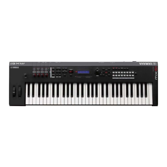
MX61/MX49 ■ PANEL LAYOUT (パネルレイアウト) The illustration is of the MX49; however, the controls and terminals of the MX61 are the same. (イラストは代表して MX49 のみを掲載しています) Rear view Front view ❺ ❽ ❾ ⓫ ⓬ ⓰ ⓲ ⓳ ❶ ❹ ❻... -
Page 6: Circuit Board Layout & Wiring (ユニットレイアウト&結線図
MX61/MX49 ■ CIRCUIT BOARD LAYOUT & WIRING (ユニットレイアウト&結線図) ● MX61 Upper case assembly (上ケース Ass'y) Wheel assembly (ホイール Ass'y) DC-IN Lower key bed assembly (下ケース鍵盤 Ass'y) Connector Unit Name Location Part No. Destinations Remarks Assembly ① UPPER CASE ASSEMBLY U230... - Page 7 MX61/MX49 ● MX49 Upper case assembly (上ケース Ass'y) Wheel assembly (ホイール Ass'y) DC-IN Lower key bed assembly (下ケース鍵盤 Ass'y) Connector Unit Name Location Part No. Destinations Remarks Assembly ① UPPER CASE ASSEMBLY U230 (ZC89480) DM-PNA DM – CN303 *1 *5 PNA – CN601 *1 *5 10P 170mm ②...
-
Page 8: Disassembly Procedures (分解手順
MX61/MX49 ■ DISASSEMBLY PROCEDURES (分解手順) Disassembly procedures of the MX61 and MX49 are almost MX61 と MX49 の分解手順はほぼ同じです。そのため、こ the same. こでは代表として MX61 の分解手順を説明します。 For that reason, we explain disassembly procedure of the MX61 as a representative here. Caution: Be sure to attach the removed filament tape just 注意:... - Page 9 MX61/MX49 JK Circuit Board 2. JK シート (Time required: About 3 minutes) (所要時間:約 3 分) Remove the upper case assembly. (See procedure 1.) 2-1 上ケース Ass'y を外します。 (1 項参照) Remove the six (6) screws marked [U220A]. The JK 2-2 [U220A]のネジ 6 本を外し、JK シートを外します。...
- Page 10 MX61/MX49 PNA Circuit Board 6. PNA シート (Time required: About 4 minutes) (所要時間:約 4 分) Remove the upper case assembly. (See procedure 1.) 6-1 上ケース Ass'y を外します。 (1 項参照) Remove the five (5) screws marked [U220E]. Then 6-2 [U220E]のネジ 5 本を外し、JK シート Ass'y を外...
- Page 11 MX61/MX49 LCD Assembly 8. LCD Ass'y (Time required: About 4 minutes) (所要時間:約 4 分) Remove the upper case assembly. (See procedure 1.) 8-1 上ケース Ass'y を外します。 (1 項参照) Remove the DM circuit board assembly and DC-IN 8-2 DM シート Ass'y と DC-IN シートを外します。...
- Page 12 MX61/MX49 White and black keys 10. 鍵盤 Ass'y の分解 (Time required: About 12 minutes) (所要時間:約 12 分) 10-1 Remove the upper case assembly. (See procedure 1.) 10-1 上ケース Ass'y を外します。 (1 項参照) 10-2 White Keys and Black Keys 10-2 白鍵、黒鍵...
- Page 13 MX61/MX49 10-3 Rubber Contact 10-3 接点ゴム 10-3-1 Remove the white and black keys corresponding to 10-3-1 外そうとしている接点ゴムに対応した白鍵・黒鍵を the rubber contacts to be removed. 外します。 (図 6、図 7、10-2 項参照) (See Fig. 6, Fig. 7 and Procedure 10-2.) 10-3-2 それぞれの接点ゴムを外します。 (図 7、写真 4) 10-3-2 Remove the rubber contacts. (Fig. 7, Photo 4) 10-4 ...
-
Page 14: Lsi Pin Description (Lsi 端子機能表
MX61/MX49 ■ LSI PIN DESCRIPTION (LSI 端子機能表) CONTENTS (目次) • AK4385ET (X6040A01) DAC (Digital to Analog Converter) ..............14 • R8A02042BG (YC479A00) SWX08 ......................15 • TAS1020BPFBR (YA413A00) USB CONTROLLER ................14 • TMP89FM42AUG (YC778D00) MICROCONTROLLER ................. 17 • μPD780031AYGK-N09-9ET-A (XZ916300) LED/SWITCH DRIVER ............17 •... - Page 15 MX61/MX49 • R8A02042BG (YC479A00) SWX08 DM: IC101...
- Page 16 MX61/MX49...
- Page 17 MX61/MX49 • TMP89FM42AUG (YC778D00) MICROCONTROLLER DM: IC402 NAME FUNCTION NAME FUNCTION – Ground I/O Port 42 High frequency departure pendulum connection terminal I/O Port 43 XOUT O High frequency departure pendulum connection terminal I/O Port 44 MODE Terminal for shipment examination / Please fix at “L” level I/O Port 45 –...
-
Page 18: Circuit Boards (シート基板図
MX61/MX49 ■ CIRCUIT BOARDS (シート基板図) CONTENTS (目次) CN Circuit Board (YE092B0) ..................19 DC-IN Circuit Board (YE093C0) ..................19 DM Circuit Board (YE094C0) ..................20 FLT Circuit Board (YE093C0) ..................19 JK Circuit Board (YE093C0) ..................25 PNA Circuit Board (YE091C0) ..................22 PNB Circuit Board (YE092B0) ..................24... - Page 19 MX61/MX49 • CN Circuit Board • DC-IN Circuit Board to DM-CN202 DC-IN Component side (部品側) Component side (部品側) 2NA-ZA59360 2NA-ZA88970 • FLT Circuit Board to DM-CN501 Component side (部品側) 2NA-ZA88970 • TOME Circuit Board • TOME2 Circuit Board Component side (部品側)...
- Page 20 MX61/MX49 • DM Circuit Board to CN-CN804 to PNA-CN601 to 61H-CN2 to 49L-CN5 to 61H-CN1 to 61L-CN5 A’ USB TO HOST USB TO DEVICE to JK-CN603 to FLT-CN901 Component side (部品側) A’ (Standby/on) MIDI 2NA-ZA67560...
- Page 21 MX61/MX49 • DM Circuit Board B’ Pattern side (パターン側) B’ 2NA-ZA67560...
- Page 22 MX61/MX49 • PNA Circuit Board MASTER VOLUME C’ KNOB TRANSPOSE FILE UTILITY FUNCTION OCTAVE EDIT PART 1-2 LINK DAW REMOTE STOP PLAY STORE SELECT C’ Component side (部品側) 2NA-ZA58780...
- Page 23 MX61/MX49 • PNA Circuit Board to PNB-CN802 to DM-CN303 to PNB-CN801 D’ to JK-CN604 to JK-CN602 to Wheel D’ Pattern side (パターン側) 2NA-ZA58780...
- Page 24 MX61/MX49 • PNB Circuit Board to PNA-CN605 INC/YES DEC/NO DATA SP L LAYER PIANO KEYBO ENTER SHIFT EXIT LEAD to PNA-CN604 E’ RHYTHM SPLIT EXT.SONG TEMPO PATTERN SAX/ BRASS KEYBOARD ORGAN STRINGS BASS GUITAR WOODWIND PART SELECT DRUM/ SOUND ETHNIC...
- Page 25 MX61/MX49 • JK Circuit Board PHONES L/MONO OUTPUT to PNA-CN606 AUX IN to DM-CN305 FOOT CONTROLLER to PNA-CN602 SUSTAIN Component side (部品側) 2NA-ZA88970...
- Page 26 MX61/MX49 • 49L Circuit Board (MX49 only) F’ to DM-CN402 to 61H-CN3 F’ Component side (部品側) 2NA-ZA13490...
- Page 27 MX61/MX49 • 49L Circuit Board (MX49 only) G’ G’ Pattern side (パターン側) 2NA-ZA13490...
- Page 28 MX61/MX49 • 61H Circuit Board to DM-CN401 to 61L-CN4 to DM-CN403 H’ Component side (部品側) H’ 2NA-V869540 • 61L Circuit Board (MX61 only) I’ to DM-CN402 to 61H-CN3 I’ Component side (部品側) 2NA-V869520...
-
Page 29: Test Program
MX61/MX49 ■ TEST PROGRAM If you execute the test no.38, Factory Set, the user's data may be lost. Therefore, back up the user's data in advance. 1. Measurement conditions 1-1 Power Supply Use PA-150A or PA-150 (AC adaptor). 1-2 Measuring instruments •... - Page 30 MX61/MX49 2. How to enter the Test Program While holding the [C2#], [F2] and [G2#] keys (C2# chord), turn the power on. While holding the number [1] and number [3] buttons on the panel, turn the power on. <MX61> [C2#]...
- Page 31 MX61/MX49 3. Test program list Test LCD display Test description, judging conditions, etc. 001: Version Displays the ROM Version. Check the version of ROM (x.xx). (OK: “B: x.xx” , “M: x.xx” , “W: x.xx” / NG: Otherwise) 002: ROM Chk1 Checks the ROM.
- Page 32 MX61/MX49 Test LCD display Test description, judging conditions, etc. 009: Output L Chk Checks the output level L. While sound is output, “ON” is displayed on the LCD. • Output Level and Cross Talk Level (PHONES) Connect the level meter to the [PHONES] terminal (L and R).
- Page 33 MX61/MX49 Test LCD display Test description, judging conditions, etc. 011: SW, LED Chk Every time each switch is pressed, confirm the following test items. • The corresponding pitch sound is output normally. • “On” is displayed on the LCD. •...
- Page 34 MX61/MX49 Test LCD display Test description, judging conditions, etc. 022: Foot Control Chk Checks the foot controller. Before executing the test, connect a foot controller (FC7) to the [FOOT CONTROLLER] terminal. Press the pedal down up to maximum, and the C3 note is output.
- Page 35 MX61/MX49 Test LCD display Test description, judging conditions, etc. 029: ROM Chk2 Checks the ROM. (Full check) Check the ROM that is connected to the CPU. (Read operation. Full Address Check SUM comparison.) After executing the test, confirm that “OK” is displayed on the LCD.
- Page 36 MX61/MX49 4. Other Inspections Turn on the [ ] (STANDBY/ON) switch to start up on the normal mode. Pop-Noise (PHONES) Connect the oscilloscope to the [PHONES] terminal (L and R). Turn on and off the [ ] (STANDBY/ON) switch sequentially.
- Page 37 MX61/MX49 ■ テストプログラム ※ テストナンバー 38 の Factory Set を実行すると、ユーザーデータが失われます。 事前にユーザーデータのバックアップを行ってください。 1. 測定条件 1-1 電源 AC アダプターは PA-150A を使用します。 1-2 測定器 ・ レベル計(JIS-C フィルタ使用) ・ 周波数カウンター(小数点以下 3 桁以上測定可能なこと) ・ オシロスコープ 注) 測定器の入力インピーダンスは 1MΩ 以上であること。 OUTPUT[L/MONO] 、 [R]端子: 10kΩ 負荷...
- Page 38 MX61/MX49 2. テストプログラムの起動 鍵盤の[C2#] 、 [F2] 、 [G2#] (C2# コード)を押しながら、 [ ] (スタンバイ/オン)スイッチを入れます。 または、 パネルのナンバー[1]と[3]のボタンを押しながら、 [ ] (スタンバイ/オン)スイッチを入れます。 <MX61> [C2#] [F2] [G2#] <MX49> [C2#] [F2] [G2#] 2-1 テストの進め方 1) テストプログラムが起動されると、LCD 上に TEST が表示されます。 TEST が表示されている状態で[ENTER]ボタンを押し、項目選択モードに入ります。 2) [ INC]/[DEC]ボタン、または[DATA]ダイアルでテスト項目を選択します。...
- Page 39 MX61/MX49 3. テスト一覧 テスト LCD 表示 テスト内容及び判定条件 001:Version バージョン表示 ROM のバージョン(x.xx)を確認します。 (OK: B:x.xx 、 M:x.xx 、 W:x.xx / NG:それ以外) 002:ROM Chk1 ROM 簡易チェック CPU に接続される ROM を検査します。 (全アドレス線、全データバス線のリード動作) テスト実行後、LCD 上に OK が表示されることを確認します。 (OK: OK / NG: NG ) 注: テスト No.6(全メモリ簡易チェック)をすれば、このテストは省略出来ます。...
- Page 40 MX61/MX49 テスト LCD 表示 テスト内容及び判定条件 009:Output L Chk OUTPUT L 端子チェック。発音中は LCD に ON が表示されます。 • 出力レベルとクロストーク量(PHONES) [PHONES]端子の L、R にレベル計を接続します。 出力レベルが下記の通りであることを確認します。 PHONES L 側:-4.6dBu ± 2dB PHONE SR 側:-62.0dBu 以下 • 出力レベルとクロストーク量(OUTPUT) OUTPUT 端子[L/MONO] 、 [R]にレベル計を接続します。 ジャックは[L/MONO] 、 [R]両方同時に挿入します。 出力レベルが下記の通りであることを確認します。 OUTPUT L 側:+1.4dBu ± 2dB OUTPUT R 側:-62.0dBu 以下...
- Page 41 MX61/MX49 テスト LCD 表示 テスト内容及び判定条件 013:Red LED On 赤色 LED 全点灯チェック 全ての赤色 LED が同時に点灯します。 点灯 LED が全て赤色であることを確認します。 014:Green LED On 緑色 LED 全点灯チェック 全ての緑色 LED が同時に点灯します。 点灯 LED が全て緑色であることを確認します。 015:All LCD On Chk LCD 全点灯チェック LCD の全ドットが点灯します。 LCD 画面全体が白くなることを確認します。 016:All LCD Off Chk LCD 全消灯チェック LCD の全ドットが消灯します。 LCD 画面全体が青くなることを確認します。 017:LCD Contrast Chk LCD コントラストチェック...
- Page 42 MX61/MX49 テスト LCD 表示 テスト内容及び判定条件 023:Sustain Chk サスティンペダルチェック [SUSTAIN]端子には、何も接続せずに検査を開始します。 検査を開始すると、 No pedal が表示されます。 フットペダル(FC3)を接続します。 フットペダルを押すと、C3 が発音されます。 次に、放すと、G3 が発音されます。 テスト実行後、LCD 上に OK が表示されることを確認します。 ( FS Down:yy 、 FS Up:yy )/ yy:現在値 (OK: OK ) 024:MIDI Chk MIDI 端子チェック テストに先立ち、MIDI[IN] 、 [OUT]端子をケーブルで接続しておきます。 テストを実行すると、C4 が発音されます。 テスト実行後、LCD 上に OK が表示されることを確認します。...
- Page 43 MX61/MX49 テスト LCD 表示 テスト内容及び判定条件 031:Wave ROM Chk2 Wave ROM フルチェック。このテストは約 2 分間かかります。 音源に接続される Wave ROM を検査します。 (リード動作。フルアドレスのチェックサム比較) テスト実行後、LCD 上に OK が表示されることを確認します。 このテスト中は LCD に Now Executing 表示が点滅します。 (OK: OK / NG: NG ) 032:Effect RAM Chk2 Effect RAM フルチェック。このテストは約 30 秒間かかります。 音源に接続される Eff ect RAM を検査します。 (全領域でのリード/ライト動作) テスト実行後、LCD 上に OK が表示されることを確認します。...
- Page 44 MX61/MX49 4. その他の検査 [ ] (スタンバイ/オン)スイッチを押して通常モードで起動します。 ポップノイズ(PHONES) オシロスコープを[PHONES]端子の L、R に接続します。 [ ] (スタンバイ/オン)スイッチを続けて ON/OFF します。 ポップノイズレベルが下記の通りであることを確認します。 PHONES L 側: 500mVp-p 以下 PHONES R 側: 500mVp-p 以下 ポップノイズ(OUTPUT) オシロスコープを[OUTPUT]端子の[L/MONO] 、 [R]に接続します。 ジャックは[L/MONO] 、 [R]両方同時に挿入します。 [ ] (スタンバイ/オン)スイッチを続けて ON/OFF します。 ポップノイズレベルが下記の通りであることを確認します。 OUTPUT L 側: 500mVp-p 以下...
- Page 45 MX61/MX49 Table1 (表 1) Switch Test Item List (SW テスト一覧表) Switch Name Display SW Code (HEX) LED to be lit Note Code Note (HEX) (順序) (SW 名) (表示) (SW コード(16 進) ) (点灯させる LED) (ノートコード) (ノート(16 進) ) KNOB FUNCTION...
-
Page 46: User Data Backup (ユーザーデータのバックアップ
MX61/MX49 ■ USER DATA BACKUP (ユーザーデータのバックアップ) You can save all data of the User memory—containing Performances, パフォーマンスやユーザーボイス、ユーティリティー設定な created User Voices, and Utility settings—to USB fl ash memory as どのユーザーメモリー上のすべてのデータを「All(オール) 」 an “All” fi le (extension: .X5A). ファイル(拡張子:.X5A)として USB フラッシュメモリー 上に保存します。... -
Page 47: Factory Set (ファクトリーセット
MX61/MX49 ■ FACTORY SET (ファクトリーセット) The original factory settings of this synthesizer’s User Memory MX49/MX61 には、ユーザーメモリーを初期化して工場出荷 can be restored as described here. The Performances, User Voices, 時の状態に戻すファクトリーセットという機能があります。 and Utility settings of the User Memory will be reset to the initial これにより、ユーザーメモリー上にあるパフォーマンスや... -
Page 48: Program Installation Procedure
MX61/MX49 ■ PROGRAM INSTALLATION PROCEDURE [Caution !] • Check to ensure that the USB memory is connected in the correct direction. (Incorrect connection will cause damage to the USB [TO DEVICE] terminal.) • Don’t turn off the power during installation. - Page 49 MX61/MX49 4. The installer is activated. Press [ ] (Play/Pause) button, and the version of the program to be installed is displayed. “X.XX” represents the version, likewise hereafter. 5. Press [ ] (Play/Pause) button, and installation will start. During installation, the progress of installation is displayed on the screen.
- Page 50 MX61/MX49 Troubleshooting Case Correction The power is shut off or Re-installation is required. the USB memory was removed during operation. (Perform the installation procedure all over again.) An error message appears on the screen Check each of the following items.
- Page 51 MX61/MX49 Messages after starting installation Message Meaning This message is displayed when: [PLAY]: Install Installation starts with the [ ] (Play/Pause) button. The installer is activated. (to the screen to confirm the program version) [PLAY]: Install ver.X.XX Installation is executed Execution of installation is confirmed.
- Page 52 MX61/MX49 ■ プログラムインストール手順 【注意!】 • USB メモリーの接続向きを確認してください。 (正しく接続しないと USB [TO DEVICE]端子を破損する原因となります。 ) • 作業中に電源を切らないでください。 • 作業中に USB メモリーを抜かないでください。 1. 書き換え用データ(MX4961SETUP.PRG)が入った USB メモリーを、USB [TO DEVICE] 端子に接続します。 <後側> USB メモリー 2. [ ] (プレイ/ポーズ)ボタンを押しながら、 [ ] (スタンバイ/オン)スイッチをオン にします。 <後側> [ ] (スタンバイ/オン)スイッチ <前側> [ ] (プレイ/ポーズ)ボタン 以下の表示が出るまで押し続けてください。...
- Page 53 MX61/MX49 4. インストーラが起動します。 [ ] (プレイ/ポーズ)ボタンを押すと、インストールするプログラムのバージョンが表示されます。 ※ X.XX の部分にバージョンが入ります。 以降、同様に表記します。 5. [ ] (プレイ/ポーズ)ボタンを押して、インストールを開始します。 インストール中は、画面に作業の進行状況が表示されます。 インストールが完了すると、以下の画面が表示されます。 6. [ ] (スタンバイ/オン)スイッチをオフにし、USB メモリーを取り外します。 7. バージョンを確認します。 7-1. テストプログラムを起動します。 (38 ページ参照) 7-2. [ENTER]ボタンを 1 回押し、 001:Version を表示させます。 7-3. 再度[ENTER]ボタンを押してバージョンを表示させ、バージョンアップされたことを確認します。 7-4. Factory Set を実行する場合は、 [ENTER]ボタンで項目選択画面に戻り、 038 : Factory Set を選択して実行します。...
- Page 54 MX61/MX49 トラブルシューティング 現象 解決方法 作業中に電源が切れた、または USB メモリを抜いて 再インストールが必要 しまった (インストール手順の最初から再実行してください) 画面上にエラーメッセージが出て、インストールが実行 以下を確認します できない ・ USB メモリが正しく挿入されているか ・ USB メモリの端子にゴミなどが付着していないか ・ 書き換え用データが、USB メモリのルートにあるか ・ USB メモリ内のデータ、もしくは USB メモリ自体が壊れていないか (別の USB メモリにて再度インストールしてみてください) ・ 書き換え用データとモデルが一致しているか インストーラ起動までのメッセージ 表示メッセージ 意 味...
- Page 55 MX61/MX49 インストール開始後のメッセージ 表示メッセージ 意味 状況・状態 [PLAY] : Install [ ] (プレイ/ポーズ)ボタンで インストーラ起動後 インストールを開始 (プログラムバージョン確認画面へ) [PLAY] : Install ver.X.XX [ ] (プレイ/ポーズ)ボタンで インストール実行確認 インストールを実行 (X.XX:プログラムバージョン) Completed. インストールが完了 インストール完了時 Program is ver.X.XX. (X.XX:プログラムバージョン) Data read error! データ読み込みエラー! 読み込みエラー (データが不正で読み込めない) Data checksum error! データチェックサムエラー! 読み込みエラー (データのチェックサムが不正) Data address error! データアドレスエラー! 読み込みエラー (データのアドレスが不正)...
-
Page 56: System Booting Flowchart
“YAMAHA MX” “MUSIC SYNTHESIZER” Stops communication with EBUS. EICN=L (IC101, C12) “YAMAHA MX” “(c) Yamaha Corp.” If opening screen display Starts USB-Func does not start, IC105 and (StreamContrl) 106 may be defective. /USBC-RES cancel Starts IC (IC304) operation... - Page 57 MX61/MX49 ■ 起動フローチャート Power On ポート初期設定 DAC-IC=L ( IC310、 5) IC107 へのアクセスが始まる /MIDI-E=L ( IC101、 D13) IC107 へのアクセスが始まら CPU 各種レジスタ設定 ない場合は、 IC101 が不良の コントラストを変更 可能性あり コントラスト設定 IC105、 106 へのアクセスが LCDCONT̲A-C= 011 始まる LCD̲CONT=3 ( IC205、 9、 10、 11) BOOT 用 SDRAM 初期化...
-
Page 58: Dm Circuit Board Check Method
MX61/MX49 ■ DM CIRCUIT BOARD CHECK METHOD The DM Circuit Board is provided with test points for service check purposes. Check the test points on the DM Circuit Board if the following symptoms appear. Symptoms and check items -- >... -
Page 59: Dm シートチェック方法
MX61/MX49 ■ DM シートチェック方法 DM シートにはサービスチェック用のテストポイントを設けてあります。 下記の症状により DM シートのテストポイントを確認してください。 症状により以下の箇所を確認します。 1. 電源を入れても LCD が点灯しない ⇒ ① 〜 ④ 及び ⑦ を順番に確認する。 2. 音が出ない、音が歪む ⇒ ⑤、⑥、⑧ 及び ⑨ を順番に確認する。 テストポイントチェック 不良が疑われる テストポイント 機能名 回路 判定基準 測定 GND 測定器具 部品 デジタル回路用 DGND ① TL505 5.0V ± 0.5V テスター IC502 5V 電源... -
Page 60: Parts List
MX61/MX49 MUSIC SYNTHESIZER PARTS LIST ■ CONTENTS (目次) MX61 OVERALL ASSEMBLY ..........2 (MX61 総組立) MX49 OVERALL ASSEMBLY ..........4 (MX49 総組立) DM CIRCUIT BOARD ASSEMBLY ........6 (DM シート Ass'y) JK CIRCUIT BOARD ASSEMBLY ........7 (JK シート Ass'y)... -
Page 61: Mx61 Overall Assembly (Mx61 総組立
MX61/MX49 ■ MX61 OVERALL ASSEMBLY (MX61 総組立) U190 Upper case assembly U210 (上ケース Ass'y) U110 Wheel assembly: See page 8 U220 U120 U220 (ホイール Ass'y: 8 ページ参照) U200 U170 U220 U220 JK circuit board assembly: U180 See page 7 (JK シート Ass'y:... - Page 62 DVD-ROM 12CM D V D − R O M (X8844I0) Y E 6 12 A 0 0 OPTICAL DISK CD-ROM MX49/MX61 MANUAL C D − R O M ⚠ W R 5 2 6 8 01 AC ADAPTOR PA-150A J A...
-
Page 63: Mx49 Overall Assembly (Mx49 総組立
MX61/MX49 ■ MX49 OVERALL ASSEMBLY (MX49 総組立) U210 Upper case assembly (上ケース Ass'y) U220 U110 U210 U120 U220 U200 U170 U190 U220 U180 U220 Wheel assembly: See page 8 U260 (ホイール Ass'y: U220 U250 U160 U220 8 ページ参照) U220 U230 U220... - Page 64 DVD-ROM 12CM D V D − R O M (X8844I0) Y E 6 12 A 0 0 OPTICAL DISK CD-ROM MX49/MX61 MANUAL C D − R O M ⚠ W R 5 2 6 8 01 AC ADAPTOR PA-150A J A...
-
Page 65: Dm Circuit Board Assembly (Dm シート Ass'y
(接続) LOCK AFTER WIRE TREATMENT (束線処理の後、 ロックする) INSERT (挿入) MATCHING SURFACE (合わせ面) MX61 only * THE SCREW HERE HAS TO BE TIGHTENED FIRSTLY D110 MX61 only (1 番最初にネジ締めのこと) STICK D100 MX61 only (貼る) MOUNTING INSTRUCTION (取付詳細) INSERT (挿入) TURN 90 DEGREE (90 度回転)... -
Page 66: Jk Circuit Board Assembly (Jk シート Ass'y
MX61/MX49 ■ JK CIRCUIT BOARD ASSEMBLY (JK シート Ass'y) MATCHING SURFACE (合わせ面) MX61 only STICK (貼る) INSERT (挿入) MX61 only J60 MX61 only PART NO. DESCRIPTION 部 品 名 REMARKS REF NO. QTY RANK JK CIRCUIT BOARD ASSEMBLY MX61 (ZD71830) J... -
Page 67: Wheel Assembly (ホイール Ass'y
MX61/MX49 ■ WHEEL ASSEMBLY (ホイール Ass'y) Accessories for VR (VR 付属品) Modulation Wheel (モジュレーションホイール) Accessories for VR (VR 付属品) Pitch Bend Wheel (ピッチベンドホイール) PART NO. DESCRIPTION 部 品 名 REMARKS REF NO. QTY RANK WV7040 0 0 WHEEL ASSEMBLY MX61,MX49 ホ... -
Page 68: Mx61 Keyboard Assembly (Mx61 16N-C61-2M 鍵盤
MX61/MX49 ■ MX61 KEYBOARD ASSEMBLY (MX61 16N-C61-2M 鍵盤) PART NO. DESCRIPTION 部 品 名 REMARKS REF NO. QTY RANK KEYBOARD UNIT 16N C61 P2M MX61 (ZF28650) 1 6 N − C 6 1 − 2 M 鍵 盤 V 3 4 1 2 6 0 0 WHITE KEY CEGB 白... -
Page 69: Mx49 Keyboard Assembly (Mx49 16N-C49 鍵盤
MX61/MX49 ■ MX49 KEYBOARD ASSEMBLY (MX49 16N-C49 鍵盤) 200 200 190 180 PART NO. DESCRIPTION 部 品 名 REMARKS REF NO. QTY RANK KEYBOARD UNIT 16N C49 D2M I MX49 (ZA13470) 1 6 N − C 4 9 鍵 盤 V 3 4 1 2 6 0 0 WHITE KEY CEGB 白... -
Page 70: Electrical Parts (電気部品
MX61/MX49 ■ ELECTRICAL PARTS (電気部品) PART NO. DESCRIPTION 部 品 名 REMARKS REF NO. QTY RANK ELECTRICAL PARTS 電 気 部 品 MX61/MX49 Z A 6 7 5 6 0 0 CIRCUIT BOARD D M シ ー ト (YE094C0) Z A 8 2 8 8 0 0 CIRCUIT BOARD DC-IN D... - Page 71 MX61/MX49 PART NO. DESCRIPTION 部 品 名 REMARKS REF NO. QTY RANK C319 U S 6 2 5 10 0 CERAMIC CAPACITOR (CHIP) 0.1uF 10V K チ ッ プ セ ラ ( B J ) C322 U S 6 6 1 6 8 0 CERAMIC CAPACITOR (CHIP)
- Page 72 MX61/MX49 PART NO. DESCRIPTION 部 品 名 REMARKS REF NO. QTY RANK C523 U S 6 6 2 2 2 0 CERAMIC CAPACITOR-B (CHIP) 220pF 50V K チ ッ プ セ ラ ( B ) C525 V 8 0 8 5 4 0 0 CERAMIC CAPACITOR-B (CHIP) 0.1uF 25V K...
- Page 73 MX61/MX49 PART NO. DESCRIPTION 部 品 名 REMARKS REF NO. QTY RANK IC204 X 3 8 2 4 A 0 0 IC SN74AHCT08PWR I C AND GATE IC204 X 3 5 8 6 B 0 0 IC TC74VHCT08AFT EL,K I...
- Page 74 MX61/MX49 PART NO. DESCRIPTION 部 品 名 REMARKS REF NO. QTY RANK R148 R D 4 5 7 10 0 CARBON RESISTOR (CHIP) 10K 1/16W J チ ッ プ 抵 抗 -156 R D 4 5 7 10 0 CARBON RESISTOR (CHIP) 10K 1/16W J チ...
- Page 75 MX61/MX49 PART NO. DESCRIPTION 部 品 名 REMARKS REF NO. QTY RANK R361 R D 4 5 7 10 0 CARBON RESISTOR (CHIP) 10K 1/16W J チ ッ プ 抵 抗 -363 R D 4 5 7 10 0 CARBON RESISTOR (CHIP) 10K 1/16W J チ...
- Page 76 MX61/MX49 PART NO. DESCRIPTION 部 品 名 REMARKS REF NO. QTY RANK R531 R D 4 5 74 7 R CARBON RESISTOR (CHIP) 47K 1/16W J チ ッ プ 抵 抗 R532 R D 15 6 15 R CARBON RESISTOR (CHIP) 1.5K 1/4W J...
- Page 77 MX61/MX49 DM, DC-IN, FLT and JK PART NO. DESCRIPTION 部 品 名 REMARKS REF NO. QTY RANK RA301 WH21060 0 RESISTOR ARRAY 3.3K x4 抵 抗 ア レ イ RA401 WH21260 0 RESISTOR ARRAY 22Kx4 抵 抗 ア レ イ...
- Page 78 MX61/MX49 DC-IN, FLT and JK PART NO. DESCRIPTION 部 品 名 REMARKS REF NO. QTY RANK C643 U R 8 3 74 7 0 ELECTROLYTIC CAP. 47uF ケ ミ コ ン C644 WW67490 0 MONOLITHIC CERAMIC CAPACITOR 0.1uF 50V K 積...
- Page 79 MX61/MX49 DC-IN, FLT, JK and PNA PART NO. DESCRIPTION 部 品 名 REMARKS REF NO. QTY RANK R609 VC 7 2 8 8 0 0 METAL OXIDE FILM RESISTOR 1W J 酸 化 金 属 被 膜 抵 抗 R610 H F 4 5 7 12 R CARBON RESISTOR 12K 1/4W J カ...
- Page 80 MX61/MX49 PART NO. DESCRIPTION 部 品 名 REMARKS REF NO. QTY RANK C618 WG88830 0 MONOLITHIC CERAMIC CAP.(CHIP) 10uF 6.3V K チ ッ プ 積 層 セ ラ コ ン C619 U S 0 3 5 10 0 CERAMIC CAPACITOR-B (CHIP) 0.1uF 16V K...
- Page 81 MX61/MX49 PNA, CN, PNB, TOME and TOME2 PART NO. DESCRIPTION 部 品 名 REMARKS REF NO. QTY RANK R663 R D 3 5 6 10 0 CARBON RESISTOR (CHIP) 1.0K 1/16W J チ ッ プ 抵 抗 -670 R D 3 5 6 10 0 CARBON RESISTOR (CHIP) 1.0K 1/16W J...
- Page 82 MX61/MX49 CN, PNB, TOME, TOME2, 61H, 61L and 49L PART NO. DESCRIPTION 部 品 名 REMARKS REF NO. QTY RANK SW806 WG31840R TACT SWITCH SKRGAMD010 タ ク ト ス イ ッ チ TEMPO SW807 WG31840R TACT SWITCH SKRGAMD010 タ ク...
- Page 83 MX61/MX49 MUSIC SYNTHESIZER CIRCUIT DIAGRAM ■ CONTENTS (目次) BLOCK DIAGRAM ............ 3 (ブロックダイアグラム) OVERALL CIRCUIT DIAGRAM (総回路図) DM 1/5 ....................... P .1 2/5 ....................... P .2 3/5 ....................... P .3 4/5 ....................... P .4 5/5 ....................... P .5 JK, DC-IN, FLT ................... P .6 PNA ......................
- Page 84 809–824 S4,S5 (C2–B3) KEYBOARD CN801 (8P) CN802 (10P) (MX49 only) CN604 (8P) CN605 (10P) CN603 (5P) CN5 (7P) (MX49/MX61: C4–C6) Charactor LCD (20 x 2) (C1–B3) 7seg x 3LED LD717 16N61,49,25KEY SW701–715 LD701–709, IC601 (MX61 only) 711, 712, 715 (In the case 49KEY Note12 Block 10 TR601–608,610–617...
- Page 85 <P.1> MX61/MX49 OVERALL CIRCUIT DIAGRAM 1/9 (総回路図 1/9) (DM 1/5) REGULATOR SDRAM 16M FLASH ROM 16M SDRAM 16M RESET : Not installed (未実装) Note: See parts list for details of circuit board component parts. 注: シートの部品詳細はパーツリストをご参照ください。 WARNING Components having special characteristics are marked and must be replacedwith parts having specifications equel to those originally installed.
- Page 86 <P.2> MX61/MX49 OVERALL CIRCUIT DIAGRAM 2/9 (総回路図 2/9) (DM 2/5) to CN_CN804 <P. 8: I4> WAVE ROM 64M ANALOG MULTIPLEXER DSP SDRAM : Ceramic Capacitor (セラミックコンデンサー) : Not installed (未実装) Note: See parts list for details of circuit board component parts.
- Page 87 <P.3> MX61/MX49 OVERALL CIRCUIT DIAGRAM 3/9 (総回路図 3/9) (DM 3/5) USB AUDIO USB TO HOST REGULATOR to JK_CN603 <P. 6: I10> EEPROM PHOTO MIDI COUPLER TO DEVICE HIGH SIDE SWITCH to PNA_CN601 : Electolytic Capacitor (ケミカルコンデンサー) <P. 7: P8> : Ceramic Capacitor (セラミックコンデンサー)...
- Page 88 <P.4> MX61/MX49 OVERALL CIRCUIT DIAGRAM 4/9 (総回路図 4/9) (DM 4/5) to 49L_CN5 <P. 9: G5> to 61L_CN5 <P. 9: G4> to 61H_CN2 <P. 9: G2> E-GKS to 61H_CN1 <P. 9: G1> : Ceramic Capacitor (セラミックコンデンサー) : Not installed (未実装) Note: See parts list for details of circuit board component parts.
- Page 89 <P.5> MX61/MX49 OVERALL CIRCUIT DIAGRAM 5/9 (総回路図 5/9) (DM 5/5) (Standby/on) REGULATOR to FLT_CN901 <P. 6: E12> DC/DC DC/DC : Electolytic Capacitor (ケミカルコンデンサー) : Ceramic Capacitor (セラミックコンデンサー) : Metal Film Resistor (金属皮膜抵抗) WARNING Components having special characteristics are marked and must be replacedwith parts having : Not installed (未実装)...
- Page 90 <P.6> MX61/MX49 OVERALL CIRCUIT DIAGRAM 6/9 (総回路図 6/9) (JK, DC-IN, FLT) OUTPUT SUSTAIN FOOT CONTROLLER AUX IN L/MONO PHONES to PNA_CN602 <P. 7: K11> to PNA_CN606 : Electolytic Capacitor (ケミカルコンデンサー) <P. 7: P3> : Ceramic Capacitor (セラミックコンデンサー) : Semiconductive Ceramic Capacitor ...
- Page 91 <P.7> MX61/MX49 OVERALL CIRCUIT DIAGRAM 7/9 (総回路図 7/9) (PNA) MASTER VOLUME : Ceramic Capacitor (セラミックコンデンサー) : Not installed (未実装) Note: See parts list for details of circuit board component parts. 注: シートの部品詳細はパーツリストをご参照ください。 to JK_CN602 <P. 6: F9> to PNB_CN801 <P. 8: P3>...
- Page 92 <P.8> MX61/MX49 OVERALL CIRCUIT DIAGRAM 8/9 (総回路図 8/9) (PNB, CN) DATA to PNA_CN604 <P. 7: B4> to DM_CN202 <P. 2: B4> to PNA_CN605 <P. 7: B5> 28CC1-2001099981 SHIFT EXIT INC/YES LAYER SPLIT RHYTHM PATTERN EXT.SONG TEMPO PART SELECT DEC/NO PIANO KEYBOARD...
- Page 93 OVERALL CIRCUIT DIAGRAM 9/9 (総回路図 9/9) (49L, 61H, 61L) (MX49/MX61: C4–C6) to DM_CN401 <P. 4: L6> to DM_CN403 <P. 4: A4> 28CC1-8822437 In the case of MX49 In the case of MX61 (C1–B3) (MX61 only) to DM_CN402 <P. 4: A3> 28CC1-8822436 (C2–B3) (MX49 only) : Not installed (未実装)...