Table of Contents
Advertisement
Quick Links
Advertisement
Table of Contents

Related Manuals for Texas Instruments LMK04808B


Summary of Contents for Texas Instruments LMK04808B
- Page 1 LMK048xx Evaluation Board User's Guide August 2011 SNAU076B Revised August 2014...
- Page 2 Low-Noise Clock Jitter Cleaner with Dual Loop PLLs Evaluation Board Operating Instructions SNAU076B LMK04800 Family Revised - August 2014 Copyright © 2014, Texas Instruments Incorporated www.ti.com...
-
Page 3: Table Of Contents
............................5 VAILABLE AMILY EVICES QUICK START ..................................6 ........................7 EFAULT OADER ODES FOR VALUATION OARDS EXAMPLE: USING CODELOADER TO PROGRAM THE LMK04808B ....................8 1. S ............................... 8 TART OADER PPLICATION 2. S .................................... 8 ELECT EVICE 3. P ................................8... - Page 4 (CLK ) ................................41 LOCK UTPUTS LMK04808B CLKout Phase Noise ............................41 LMK04808B OSCout Phase Noise ............................43 LMK04806B CLKout Phase Noise ............................44 LMK04806B OSCout Phase Noise ............................46 LMK04803B CLKout Phase Noise ............................47 LMK04803B OSCout Phase Noise ............................49 APPENDIX C: SCHEMATICS ..............................
-
Page 5: General Description
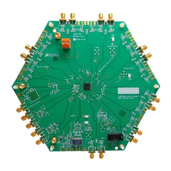
General Description The LMK048xx Evaluation Board simplifies evaluation of the LMK048xxB Low-Noise Clock Jitter Cleaner with Dual Loop PLLs. Texas Instruments Incorporated’s CodeLoader software can be used to program the internal registers of the LMK048xxB device through the USB2ANY-uWire interface. The CodeLoader software will run on a Windows 7 or Windows XP PC and can be downloaded from http://www.ti.com/tool/codeloader/. -
Page 6: Quick Start
CodeLoader can be downloaded from http://www.ti.com/tool/codeloader. 5. Measurements may be made on an active output clock port via its SMA connector. Figure 1: Quick Start Diagram SNAU076B LMK04800 Family Revised - August 2014 Copyright © 2014, Texas Instruments Incorporated www.ti.com... -
Page 7: Default Codeloader Modes For Evaluation Boards
Table 3 may be restored by clicking “Mode” and selecting the appropriate device configuration, as shown in Figure 2 in the case of the LMK04808B device. Similar default modes are available for each LMK048xxB device in CodeLoader. Choose a mode with CLKin0 for differential clock signal or CLKin1 for a single ended signal. -
Page 8: Example: Using Codeloader To Program The Lmk04808B
The purpose of this section is to walk the user through using CodeLoader 4 to make some measurements with the LMK04808B device as an example. For more information on CodeLoader refer to Appendix A: CodeLoader Usage or the CodeLoader 4 instructions located at http://www.ti.com/tool/codeloader. -
Page 9: Restoring A Default Mode
Information contains information on troubleshooting communications. 4. Restoring a Default Mode Click “Mode” “LMK04808B, 122.88 MHz VCXO, 122.88 MHz CLKin1”; then press Ctrl+L. Figure 5: Setting the Default mode for LMK04808 For the purpose of this walkthrough, a default mode will be loaded to ensure a common starting point. -
Page 10: Visual Confirmation Of Frequency Lock
A balun may also be used. Ensure CLKoutX and CLKoutX* states are Figure 7: Setting LVCMOS modes SNAU076B LMK04800 Family Revised - August 2014 Copyright © 2014, Texas Instruments Incorporated www.ti.com... - Page 11 5. The phase noise may be measured with a spectrum analyzer or signal source analyzer. See Appendix B: Typical Phase Noise Performance Plots for phase noise plots of the clock outputs. Texas Instruments Incorporated’s Clock Design Tool can be used to calculate divider values to achieve desired clock output frequencies. See: http://www.ti.com/tool/clockdesigntool.
-
Page 12: Pll Loop Filters And Loop Parameters
The following tables contain the parameters for PLL1 and PLL2 for each oscillator option. Texas Instruments Incorporated’s Clock Design Tool can be used to optimize PLL phase noise/jitter for given specifications. See: http://www.ti.com/tool/clockdesigntool/. -
Page 13: Pll2 Loop Filter
Bandwidth Note: PLL Loop Bandwidth is a function of Kφ, Kvco, N as well as loop components. Changing Kφ and N will change the loop bandwidth. Revised - August 2014 LMK04800 Family SNAU076B Copyright © 2014, Texas Instruments Incorporated www.ti.com... -
Page 14: Evaluation Board Inputs And Outputs
All LVPECL clock outputs are source-terminated using 240-ohm resistors. If an output pair is programmed to LVCMOS, each output can be independently configured (normal, inverted, or off/tri-state). SNAU076B LMK04800 Family Revised - August 2014 Copyright © 2014, Texas Instruments Incorporated www.ti.com... - Page 15 On-board LDO regulators and 0 Ω resistor options provide flexibility to supply and route power to various devices. See schematics for more details. Revised - August 2014 LMK04800 Family SNAU076B Copyright © 2014, Texas Instruments Incorporated www.ti.com...
- Page 16 Populated: Power, VccVCXO/Aux input can power these circuits directly VccVCXO/Aux Input or supply the on-board LDO regulators. 0 Ω resistor options provide flexibility to route power. SNAU076B LMK04800 Family Revised - August 2014 Copyright © 2014, Texas Instruments Incorporated www.ti.com...
- Page 17 CodeLoader: • MODE = (3) Dual PLL, Ext VCO (Fin), (5) Dual PLL, Ext VCO, 0-Delay, (11) PLL2, Ext VCO (Fin) Revised - August 2014 LMK04800 Family SNAU076B Copyright © 2014, Texas Instruments Incorporated www.ti.com...
- Page 18 The programmable logic I/O signals accessible through CLKuWIRE_TP this header include: SYNC, Status_Holdover, LEuWIRE_TP Status_LD, Status_CLKin0, and Status_CLKin1. These logic I/O signals also have dedicated SMAs and test points. SNAU076B LMK04800 Family Revised - August 2014 Copyright © 2014, Texas Instruments Incorporated www.ti.com...
- Page 19 Note: Before a high-frequency internal signal (e.g. PLL divider output signal) is selected by HOLDOVER_MUX, it is suggested to first remove the 270 ohm resistor to prevent the LED from loading the output. Revised - August 2014 LMK04800 Family SNAU076B Copyright © 2014, Texas Instruments Incorporated www.ti.com...
- Page 20 Status_CLKinX pin can be programmed on the Bits/Pins tab via the Status_CLKinX_MUX control. Refer to the LMK04800 Family Datasheet section “Status Pins” for more information. SNAU076B LMK04800 Family Revised - August 2014 Copyright © 2014, Texas Instruments Incorporated www.ti.com...
- Page 21 When SYNC_MUX is 3 to 6 (pin enabled as output), a status signal for the SYNC pin can be selected on the Bits/Pins tab via the SYNC_MUX control. Revised - August 2014 LMK04800 Family SNAU076B Copyright © 2014, Texas Instruments Incorporated www.ti.com...
-
Page 22: Recommended Test Equipment
50-ohm cables to minimize external sources of skew or other errors/distortion that may be introduced if using oscilloscope probes. SNAU076B LMK04800 Family Revised - August 2014 Copyright © 2014, Texas Instruments Incorporated www.ti.com... -
Page 23: Programming 0-Delay Mode In Codeloader
PLL1 VCO and PLL2 reference frequency are mismatched and the one or more of the PLLs are out of lock. While there still could be an error in the Revised - August 2014 LMK04800 Family SNAU076B Copyright © 2014, Texas Instruments Incorporated www.ti.com... - Page 24 CLKout8 Divide Actual CLKout8 245.76 MHz 122.88 MHz 245.76 MHz 61.44 MHz Output Frequency Reported CLKotu8 245.76 MHz 122.88 MHz 245.76 MHz 61.44 MHz Output Frequency SNAU076B LMK04800 Family Revised - August 2014 Copyright © 2014, Texas Instruments Incorporated www.ti.com...
-
Page 25: Single Loop 0-Delay Mode Examples
1 to 2 to reduce the PLL2 phase detector frequency from 122.88 MHz to 61.44 MHz. Now the adjusted VCO frequency can be programmed to allow PLL2 to lock. Revised - August 2014 LMK04800 Family SNAU076B Copyright © 2014, Texas Instruments Incorporated www.ti.com... - Page 26 Bypassed Bypassed CLKout8 Divide Actual CLKout8 245.76 1474.56 MHz 245.76 MHz 61.44 MHz Output Frequency Reported CLKout8 245.76 1474.56 MHz 40.96 MHz 2.56 MHz Output Frequency SNAU076B LMK04800 Family Revised - August 2014 Copyright © 2014, Texas Instruments Incorporated www.ti.com...
-
Page 27: Appendix A: Codeloader Usage
The Pin Configuration field is hardware dependent and normally does not need to be changed by the user. Figure 8 shows the default settings. Revised - August 2014 LMK04800 Family SNAU076B Copyright © 2014, Texas Instruments Incorporated www.ti.com... -
Page 28: Clock Outputs Tab
This tab also allows the user to select the VCO Divider value (2 to 8). Note that the total PLL2 N divider value is the product of the VCO Divider value and the PLL N Prescaler and N Counter SNAU076B LMK04800 Family Revised - August 2014 Copyright © 2014, Texas Instruments Incorporated www.ti.com... - Page 29 PLL(s) may be out of lock, as highlighted by the red box in Figure 10. Figure 10: Warning message indicating mismatch between PLL1 VCO frequency (30.72MHz) and PLL2 reference frequency (122.88 MHz) Revised - August 2014 LMK04800 Family SNAU076B Copyright © 2014, Texas Instruments Incorporated www.ti.com...
-
Page 30: Pll1 Tab
(MHz) This value is calculated as: PLL1 PDF = CLKin Frequency / (PLL1_R * CLKinX_PreR_DIV), where CLKinX_PreR_DIV is the predivider value of the selected input clock. SNAU076B LMK04800 Family Revised - August 2014 Copyright © 2014, Texas Instruments Incorporated www.ti.com... -
Page 31: Setting The Pll1 Vco Frequency And Pll2 Reference Frequency
PLL2 tab should be 122.88 MHz (VCXO frequency). Because of the mismatched frequencies, a warning message will indicate this condition on the Clock Outputs tab but may be disregarded in a case like this. Revised - August 2014 LMK04800 Family SNAU076B Copyright © 2014, Texas Instruments Incorporated www.ti.com... -
Page 32: Pll2 Tab
PLL2 R Counter value (1 to 4095). N Counter PLL2_N PLL2 N Counter value (1 to 262143). PLLN Prescaler PLL2_P PLL2 N Prescaler value (2 to 8). SNAU076B LMK04800 Family Revised - August 2014 Copyright © 2014, Texas Instruments Incorporated www.ti.com... -
Page 33: Bits /Pins Tab
TIP: Right-clicking any register name in the Bits/Pins tab will display a Help prompt with the register address, data bit location/length, and a brief register description. Revised - August 2014 LMK04800 Family SNAU076B Copyright © 2014, Texas Instruments Incorporated www.ti.com... - Page 34 Sets the selected signal on the Status_LD pin. LD_TYPE Sets I/O pin type on the Status_LD pin. HOLDOVER_MUX Sets the selected signal on the Status_HOLDOVER pin. SNAU076B LMK04800 Family Revised - August 2014 Copyright © 2014, Texas Instruments Incorporated www.ti.com...
- Page 35 EN_VTUNE_RAIL_DET Allows rail-to-rail operation of VCXO with default of 0. Allows use of DAC_LOW_TRIP, DAC_HIGH_TRIP. Must be used with EN_MAC_DAC = 1. CLKin_SELECT_MODE must be 4 or 6 (auto mode) to use. Revised - August 2014 LMK04800 Family SNAU076B Copyright © 2014, Texas Instruments Incorporated www.ti.com...
- Page 36 Unique divides on individual CLKinX signals allows switchover from one clock input to another clock input without needing to reprogram the PLL1_R divider to keep the device in lock. SNAU076B LMK04800 Family Revised - August 2014 Copyright © 2014, Texas Instruments Incorporated www.ti.com...
- Page 37 Enable this bit when using a PLL2 phase detector frequency > 100 MHz. SYNC Sets these pins on the uWire header to logic high Program Pins Status_CLKin0 (checked) or logic low (unchecked). Status_CLKin1 Revised - August 2014 LMK04800 Family SNAU076B Copyright © 2014, Texas Instruments Incorporated www.ti.com...
-
Page 38: Registers Tab
By clicking in the “bit field” it is possible to manually change the value of registers by typing ‘1’ and ‘0.’ SNAU076B LMK04800 Family Revised - August 2014 Copyright © 2014, Texas Instruments Incorporated www.ti.com... -
Page 39: Appendix B: Typical Phase Noise Performance Plots
PLL1 while retaining the frequency accuracy of the reference clock input. This VCXO sets the reference noise to PLL2. Figure 15 shows the open loop typical phase noise performance of the CVHD-950-122.88 Crystek VCXO. Revised - August 2014 LMK04800 Family SNAU076B Copyright © 2014, Texas Instruments Incorporated www.ti.com... -
Page 40: Clock Output Measurement Technique
Both OSCout0 and OSCout1 frequencies are 122.88 MHz since the OSCout Divider is bypassed. OSCout0 is programmed to LVCMOS mode and OSCout1 is fixed as LVPECL. SNAU076B LMK04800 Family Revised - August 2014 Copyright © 2014, Texas Instruments Incorporated www.ti.com... -
Page 41: Clock Outputs (Clkout)
245.76 MHz LVPECL16 122.88 MHz LVDS 122.88 MHz LVCMOS 122.88 MHz LVPECL16 Frequency Offset (Hz) Figure 16: LMK04808B CLKout Phase Noise Table 14: LMK04808B Phase Noise (dBc/Hz) Phase Noise and RMS Jitter (fs) 1474.56 MHz 1474.56 MHz 491.52 MHz 491.52 MHz Offset... - Page 42 For the LMK04808B, the internal VCO frequency is 2949.12 MHz. The divide-by-12 CLKout frequency is 245.76 MHz, and the divide-by-24 CLKout frequency is 122.88 MHz. Table 15: LMK04808B Phase Noise and RMS Jitter for Different CLKout Output Formats and Frequencies 245.76 245.76...
-
Page 43: Lmk04808B Oscout Phase Noise
122.88 MHz LVCMOS OSCin through CLKout 122.88 MHz OSCout0 LVPECL16 122.88 MHz OSCout1 LVPECL16 Title Figure 17: LMK04808B OSCout Phase Noise Table 16: LMK04808B OSCout Phase Noise and RMS Jitter (fs) OSCout0 OSCout1 OSCin thru Offset LVPECL LVPECL CLKout -110.2 -111.1... -
Page 44: Lmk04806B Clkout Phase Noise
100 Hz to 20 MHz For the LMK04806B, the internal VCO frequency is 2457.60 MHz. The divide-by-10 CLKout frequency is 245.76 MHz, and the divide-by-20 CLKout frequency is 122.88 MHz. SNAU076B LMK04800 Family Revised - August 2014 Copyright © 2014, Texas Instruments Incorporated www.ti.com... - Page 45 RMS Jitter (fs) 106.9 101.5 96.4 134.2 109.7 108.2 10 kHz to 20 MHz RMS Jitter (fs) 116.8 112.4 106.4 143.2 118.9 117.9 100 Hz to 20 MHz Revised - August 2014 LMK04800 Family SNAU076B Copyright © 2014, Texas Instruments Incorporated www.ti.com...
-
Page 46: Lmk04806B Oscout Phase Noise
20 MHz -157.6 -159.9 -156.9 RMS Jitter (fs) 138.4 89.7 120.0 10 kHz to 20 MHz RMS Jitter (fs) 143.7 97.3 126.2 100 Hz to 20 MHz SNAU076B LMK04800 Family Revised - August 2014 Copyright © 2014, Texas Instruments Incorporated www.ti.com... -
Page 47: Lmk04803B Clkout Phase Noise
100 Hz to 20 MHz For the LMK04803B, the internal VCO frequency is 1966.08 MHz. The divide-by-8 CLKout frequency is 245.76 MHz, and the divide-by-16 CLKout frequency is 122.88 MHz. Revised - August 2014 LMK04800 Family SNAU076B Copyright © 2014, Texas Instruments Incorporated www.ti.com... - Page 48 RMS Jitter (fs) 115.1 113.1 107.9 137.5 126.1 120.5 10 kHz to 20 MHz RMS Jitter (fs) 126.4 124.2 116.7 147.5 136.4 128.9 100 Hz to 20 MHz SNAU076B LMK04800 Family Revised - August 2014 Copyright © 2014, Texas Instruments Incorporated www.ti.com...
-
Page 49: Lmk04803B Oscout Phase Noise
20 MHz -158.1 -159.4 -157.0 RMS Jitter (fs) 107.1 92.4 119.1 10 kHz to 20 MHz RMS Jitter (fs) 111.6 98.1 123.3 100 Hz to 20 MHz Revised - August 2014 LMK04800 Family SNAU076B Copyright © 2014, Texas Instruments Incorporated www.ti.com... -
Page 50: Appendix C: Schematics
Appendix C: Schematics Power Supplies SNAU076B LMK04800 Family Revised - August 2014 Copyright © 2014, Texas Instruments Incorporated www.ti.com... -
Page 51: Lmk048Xxb Device With Loop Filter And Crystal Circuits
You should completely validate and test File: LMK048xx_PLL.SchDoc http://www.national.com your design implementation to confirm the system functionality for your application. Contact: http://www.national.com/support © Copyright, National Semiconductor, 2009 Revised - August 2014 LMK04800 Family SNAU076B Copyright © 2014, Texas Instruments Incorporated www.ti.com... -
Page 52: Reference Inputs (Clk In 0 & Clk In 1), External Vcxo (Osc In ) & Vco Circuits , And Osc Out 1 Output
Reference Inputs (CLKin0 & CLKin1), External VCXO (OSCin) & VCO Circuits, and OSCout1 Output SNAU076B LMK04800 Family Revised - August 2014 Copyright © 2014, Texas Instruments Incorporated www.ti.com... -
Page 53: Clock Outputs (Osc Out 0, Clk Out To Clk Out 3)
You should completely validate and test File: OutClks0.SchDoc http://www.national.com your design implementation to confirm the system functionality for your application. Contact: http://www.national.com/support © Copyright, National Semiconductor, 2009 Revised - August 2014 LMK04800 Family SNAU076B Copyright © 2014, Texas Instruments Incorporated www.ti.com... -
Page 54: Clock Outputs (Clkout4 To Clkout7)
You should completely validate and test File: OutClks1.SchDoc http://www.national.com your design implementation to confirm the system functionality for your application. Contact: http://www.national.com/support © Copyright, National Semiconductor, 2009 SNAU076B LMK04800 Family Revised - August 2014 Copyright © 2014, Texas Instruments Incorporated www.ti.com... -
Page 55: Clock Outputs (Clkout8 To Clkout11)
You should completely validate and test File: OutClks2.SchDoc http://www.national.com your design implementation to confirm the system functionality for your application. Contact: http://www.national.com/support © Copyright, National Semiconductor, 2009 Revised - August 2014 LMK04800 Family SNAU076B Copyright © 2014, Texas Instruments Incorporated www.ti.com... -
Page 56: Uwire Header, Logic I/O Ports And Status Leds
Header, Logic I/O Ports and Status LEDs SNAU076B LMK04800 Family Revised - August 2014 Copyright © 2014, Texas Instruments Incorporated www.ti.com... -
Page 57: Usb Interface
USB Interface Revised - August 2014 LMK04800 Family SNAU076B Copyright © 2014, Texas Instruments Incorporated www.ti.com... -
Page 58: Appendix D: Bill Of Materials
R74, R82, R84, R229, R304, R327, R329, R331, R333, R337, R340, R341, R346, R347, R349, R353, R354, R358, R361, R364, R365, R368, R371, R373, R374, R375, R400, R402 SNAU076B LMK04800 Family Revised - August 2014 Copyright © 2014, Texas Instruments Incorporated www.ti.com... - Page 59 CAP, CERM, 82pF, 50V, +/-10%, C0G/NP0, 0603 Kemet C0603C820K5GACTU C10, C29, C32, CAP, CERM, 2200pF, 50V, +/-10%, X7R, 0603 Kemet C0603C222K5RACTU C341 CAP, CERM, 10µF, 10V, +/-20%, X5R, 0805 Kemet C0805C106M8PACTU Revised - August 2014 LMK04800 Family SNAU076B Copyright © 2014, Texas Instruments Incorporated www.ti.com...
- Page 60 CAP, CERM, 1uF, 16V, +/-10%, X5R, 0603 Kemet C0603C105K4PACTU C413, C415 CAP, CERM, 0.01uF, 50V, +/-5%, X7R, 0603 Kemet C0603C103J5RACTU Cb1_B1 CAP, CERM, 0.33uF, 16V, +/-10%, X7R, 0603 Kemet C0603C334K4RACTU SNAU076B LMK04800 Family Revised - August 2014 Copyright © 2014, Texas Instruments Incorporated www.ti.com...
- Page 61 RES, 100 ohm, 5%, 0.1W, 0603 Vishay-Dale CRCW0603100RJNEA R18, R336, R342, FB, 1000 ohm, 600 mA, 0603, Ferrite Murata BLM18HE102SN1D R343 RES, 18 ohm, 5%, 0.1W, 0603 Vishay-Dale CRCW060318R0JNEA Revised - August 2014 LMK04800 Family SNAU076B Copyright © 2014, Texas Instruments Incorporated www.ti.com...
- Page 62 RES, 47k ohm, 5%, 0.1W, 0603 Vishay-Dale CRCW060347K0JNEA Rb2_B1 RES, 3.9k ohm, 5%, 0.1W, 0603 Vishay-Dale CRCW06033K90JNEA S1, S2, S3, S4, S5, 0.875" Standoff VOLTREX SPCS-14 LMK04800 Texas Instruments LMK048xxBISQ SNAU076B LMK04800 Family Revised - August 2014 Copyright © 2014, Texas Instruments Incorporated www.ti.com...
- Page 63 C39, C40, C333, Technology, Dielectric, xxV, xx% DNP_CAP Cb1_VCO, Cb2_B1, Cb2_VCO, Cb2pVCO C316, C320, C327, CAP, CERM, 0.1uF, 16V, +/-5%, X7R, 0603 Kemet C0603C104J4RACTU C328, C332, C334, C336 Revised - August 2014 LMK04800 Family SNAU076B Copyright © 2014, Texas Instruments Incorporated www.ti.com...
- Page 64 Diode, Zener, 3.3V, 150mW, SOD-523F Comchip Technology CZRU52C3V3 GND_TP, Vcc_TP DNP_TP HWB, RESET APEM Components, ADTSM31NV J400 CONN RCPT MINI USB2.0 5POS SMD Hirose Electric Co. Ltd. UX60SA-MB-5ST SNAU076B LMK04800 Family Revised - August 2014 Copyright © 2014, Texas Instruments Incorporated www.ti.com...
- Page 65 R179, R187, R204, R209, R225, R376 R6, R7, R15, R17, RES, 270 ohm, 5%, 0.1W, 0603 Vishay-Dale CRCW0603270RJNEA R31, R32, R39, R40, R49, R50, R79, R314 Revised - August 2014 LMK04800 Family SNAU076B Copyright © 2014, Texas Instruments Incorporated www.ti.com...
- Page 66 CRCW060382R0JNEA R95, R98, R101, R116, R118, R120, R123, R137, R140, R144, R146, R160, R162, R166, R168, R181, R184, R186, R189, R203, R205, R208, R211, R224, R227 SNAU076B LMK04800 Family Revised - August 2014 Copyright © 2014, Texas Instruments Incorporated www.ti.com...
- Page 67 R403, R406, R408, RES, 33 ohm, 5%, 0.1W, 0603 Vishay-Dale CRCW060333R0JNEA R409, R410 CRO2949A-LF U301 3-Terminal Adjustable Regulator Texas Instruments LM317AEMP U400, Y400 Y300, Y301 DNP_XTAL Revised - August 2014 LMK04800 Family SNAU076B Copyright © 2014, Texas Instruments Incorporated www.ti.com...
-
Page 68: Appendix E: Pcb Layers Stackup
• Bottom Layer copper clad for thermal relief (2 oz.) 12.6 mil Ground plane [LMK048xxENG.GP1] 8 mil Power plane #2 [LMK048xxENG.G3] 12 mil Bottom Layer [LMK048xxENG.GBL] SNAU076B LMK04800 Family Revised - August 2014 Copyright © 2014, Texas Instruments Incorporated www.ti.com... -
Page 69: Appendix F: Pcb Layout
Appendix F: PCB Layout Layer #1 – Top Revised - August 2014 LMK04800 Family SNAU076B Copyright © 2014, Texas Instruments Incorporated www.ti.com... -
Page 70: Layer #2 - Rf Ground Plane (Inverted)
Layer #2 – RF Ground Plane (Inverted) SNAU076B LMK04800 Family Revised - August 2014 Copyright © 2014, Texas Instruments Incorporated www.ti.com... -
Page 71: Layer #3 - Vcc Planes
Layer #3 – Vcc Planes Revised - August 2014 LMK04800 Family SNAU076B Copyright © 2014, Texas Instruments Incorporated www.ti.com... -
Page 72: Layer #4 - Ground Plane (Inverted)
Layer #4 – Ground Plane (Inverted) SNAU076B LMK04800 Family Revised - August 2014 Copyright © 2014, Texas Instruments Incorporated www.ti.com... -
Page 73: Layer # 5 - Vcc Planes 2
Layer # 5 – Vcc Planes 2 Revised - August 2014 LMK04800 Family SNAU076B Copyright © 2014, Texas Instruments Incorporated www.ti.com... -
Page 74: Layer #6 - Bottom
Layer #6 – Bottom SNAU076B LMK04800 Family Revised - August 2014 Copyright © 2014, Texas Instruments Incorporated www.ti.com... -
Page 75: Layers #1 And 6 - Top And Bottom (Composite)
Layers #1 and 6 – Top and Bottom (Composite) Revised - August 2014 LMK04800 Family SNAU076B Copyright © 2014, Texas Instruments Incorporated www.ti.com... -
Page 76: Appendix G: Evm Software And Communication: Interfacing Uwire
There are two options in communicating with the uWire interface from the computer. OPTION 1 Open Codeloader.exe Click “Select Device” Click “Port Setup” tab Click “LPT” (in Communication Mode) OPTION 2 SNAU076B LMK04800 Family Revised - August 2014 Copyright © 2014, Texas Instruments Incorporated www.ti.com... - Page 77 Open Codeloader.exe Click “Select Device” Click “Port Setup” Tab Click “USB” (in Communication Mode) *Remember to also make modifications in “Pin Configuration” Section according to Table above. Revised - August 2014 LMK04800 Family SNAU076B Copyright © 2014, Texas Instruments Incorporated www.ti.com...
-
Page 78: Appendix H: Troubleshooting Information
Redesign PLL1 loop filter with higher phase detector frequency Redesign PLL1 loop filter with higher charge pump current iii. Isolate VCXO tuning input from PLL1 charge pump with an op amp. SNAU076B LMK04800 Family Revised - August 2014 Copyright © 2014, Texas Instruments Incorporated www.ti.com... -
Page 79: 3) Confirm Pll2 Operation/Locking
5) Program LD_MUX = “PLL2 DLD” 6) Confirm the LD pin output is high. 7) Program LD_MUX = “PLL1 & PLL2 DLD” 8) Confirm the LD pin output is high. Revised - August 2014 LMK04800 Family SNAU076B Copyright © 2014, Texas Instruments Incorporated www.ti.com... - Page 80 STANDARD TERMS AND CONDITIONS FOR EVALUATION MODULES Delivery: TI delivers TI evaluation boards, kits, or modules, including any accompanying demonstration software, components, or documentation (collectively, an “EVM” or “EVMs”) to the User (“User”) in accordance with the terms and conditions set forth herein. Acceptance of the EVM is expressly subject to the following terms and conditions.
- Page 81 FCC Interference Statement for Class B EVM devices NOTE: This equipment has been tested and found to comply with the limits for a Class B digital device, pursuant to part 15 of the FCC Rules. These limits are designed to provide reasonable protection against harmful interference in a residential installation.
- Page 82 【無線電波を送信する製品の開発キットをお使いになる際の注意事項】 開発キットの中には技術基準適合証明を受けて いないものがあります。 技術適合証明を受けていないもののご使用に際しては、電波法遵守のため、以下のいずれかの 措置を取っていただく必要がありますのでご注意ください。 1. 電波法施行規則第6条第1項第1号に基づく平成18年3月28日総務省告示第173号で定められた電波暗室等の試験設備でご使用 いただく。 2. 実験局の免許を取得後ご使用いただく。 3. 技術基準適合証明を取得後ご使用いただく。 なお、本製品は、上記の「ご使用にあたっての注意」を譲渡先、移転先に通知しない限り、譲渡、移転できないものとします。 上記を遵守頂けない場合は、電波法の罰則が適用される可能性があることをご留意ください。 日本テキサス・イ ンスツルメンツ株式会社 東京都新宿区西新宿6丁目24番1号 西新宿三井ビル 3.3.3 Notice for EVMs for Power Line Communication: Please see http://www.tij.co.jp/lsds/ti_ja/general/eStore/notice_02.page 電力線搬送波通信についての開発キットをお使いになる際の注意事項については、次のところをご覧くださ い。http://www.tij.co.jp/lsds/ti_ja/general/eStore/notice_02.page SPACER EVM Use Restrictions and Warnings: 4.1 EVMS ARE NOT FOR USE IN FUNCTIONAL SAFETY AND/OR SAFETY CRITICAL EVALUATIONS, INCLUDING BUT NOT LIMITED TO EVALUATIONS OF LIFE SUPPORT APPLICATIONS.
- Page 83 Notwithstanding the foregoing, any judgment may be enforced in any United States or foreign court, and TI may seek injunctive relief in any United States or foreign court. Mailing Address: Texas Instruments, Post Office Box 655303, Dallas, Texas 75265 Copyright © 2015, Texas Instruments Incorporated...
- Page 84 IMPORTANT NOTICE Texas Instruments Incorporated and its subsidiaries (TI) reserve the right to make corrections, enhancements, improvements and other changes to its semiconductor products and services per JESD46, latest issue, and to discontinue any product or service per JESD48, latest issue.