Table of Contents
Advertisement
Quick Links
Advertisement
Table of Contents
Troubleshooting

Related Manuals for LG U8138


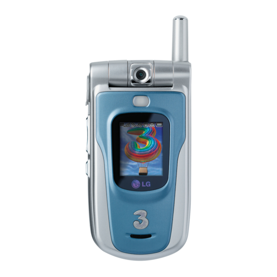
Summary of Contents for LG U8138
- Page 1 Service Manual U8138 P/N : MMBD0042101 Date: November, 2004 / Issue 1.0...
-
Page 2: Table Of Contents
Table Of Contents 1. INTRODUCTION ......6 3.2.3 Camera & Camera FPC Interface... 40 3.2.4 Camera Position Detection ..... 42 1.1 Purpose........... 6 3.2.5 Camera Regulator ......42 1.2 Regulatory Information......6 3.2.6 Display & LCD FPC Interface ..43 1.3 Abbreviations .......... - Page 3 Table Of Contents 3.8.2 Transmitter........85 4.20.1 Checking ........152 3.8.3 Frequency Generation ....89 4.20.2 Checking Ant. SW module ..152 4.20.3 Checking Control Signal ..... 152 4. TROUBLE SHOOTING ....91 4.20.4 Checking RF TX Level ....155 4.20.5 Checking PAM Block ....
- Page 4 Table Of Contents 8.3.4 DCS 1800 Calibration Items ..214 8.3.5 WCDMA Calibration Items .... 217 8.3.6 Baseband Calibration Item ... 225 8.4 Program Operation ......226 8.4.1 XCALMON Program Overview ..226 8.4.2 XCALMON Icon Description ..227 8.4.3 Calibration Procedure ....230 8.4.4 Calibration Result Message ..
-
Page 5: Introduction
1. INTRODUCTION 1. INTRODUCTION 1.1 Purpose This manual provides the information necessary to repair, calibration, description and download the features of this model. 1.2 Regulatory Information A. Security Toll fraud, the unauthorized use of telecommunications system by an unauthorized part (for example, persons other than your company’s employees, agents, subcontractors, or person working on your company’s behalf) can result in substantial additional charges for your telecommunications services. - Page 6 1. INTRODUCTION E. Notice of Radiated Emissions This model complies with rules regarding radiation and radio frequency emission as defined by local regulatory agencies. In accordance with these agencies, you may be required to provide information such as the following to the end user. F.
-
Page 7: Abbreviations
1. INTRODUCTION 1.3 Abbreviations For the purposes of this manual, following abbreviations apply: Automatic Power Control Baseband Bit Error Ratio CC-CV Constant Current – Constant Voltage Cigar Lighter Adapter Digital to Analog Converter Digital Communication System dB relative to 1 milliwatt Digital Signal Processing DeskTop Charger EEPROM... - Page 8 1. INTRODUCTION PSTN Public Switched Telephone Network Radio Frequency Receiving Loudness Rating Root Mean Square Real Time Clock Surface Acoustic Wave Subscriber Identity Module Sending Loudness Rating SRAM Static Random Access Memory UMTS Universal Mobile Telephony System - 9 -...
-
Page 9: Performance
2. PERFORMANCE 2. PERFORMANCE 2.1 System Overview Item Specification Shape GSM900/1 800 & WCDMA Folder- Dual Mode Handset Size 49.5 x 95.7 x 22.5 mm Weight 120g (with Battery) Power 1400mA Li-Polymer Over 180 Min (WCDMA, Tx=12 dBm, Voice) Talk Time Over 220 Min (GSM, Tx=Max, Voice) Over 165 hrs (WCDMA, DRX=1.28) Standby Time... -
Page 10: Usable Environment
2. PERFORMANCE 2.2 Usable environment 1) Environment Item Spec. Unit Voltage 4.0 (Typ), 3.4 (Min), (Shut Down: 3.2) Size -20 ~ + 60 °C Storage -30 ~ + 85 °C Humidity max. 85 2) Environment(Accessory) Item Spec. Typ. Unit Power Available power * CLA: 12~24V(DC) 2.3 Radio Performance... - Page 11 2. PERFORMANCE Item 30M ~ 1GHz -36dBm 30M ~ 1GHz -36dBm MS allocated 1G ~ 1710MHz -30dBm Channel 1710M ~ 1785MHz -36dBm 1G ~ 4GHz -30dBm Radiated 1785M ~ 4GHz -30dBm Spurious 30M ~ 880MHz -57dBm 30M ~ 880MHz -57dBm Emission 880M ~ 915MHz -59dBm...
- Page 12 2. PERFORMANCE Item Frequency offset 800kHz Intermodulation product should Intermodulation attenuation – be Less than 55dB below the level of Wanted signal Power control Power Tolerance Power control Power Tolerance Level (dBm) (dB) Level (dBm) (dB) ±3 ±3 ±3 ±3 ±3 ±3 ±3...
- Page 13 2. PERFORMANCE 2) Transmitter-WCDMA Mode Item Specification Class3: +24dBm(+1/-3dB) Maximum Output Power Class4: +21dBm(±2dB) Frequency Error ±0.1ppm Open Loop Power control in uplink ±9dB@normal, ±12dB@extreme Adjust output(TPC command) +0.5/1.5 +1/3 +1.5/4.5 Inner Loop Power control in uplink -0.5/+0.5 -0.5/+0.5 -0.5/+0.5 -0.5/-1.5 -1/-3 -1.5/-4.5...
- Page 14 2. PERFORMANCE Item Specification 33dB@5MHz, ACP>-50dBm Adjacent Channel Leakage Ratio(ACLR) 43dB@10MHz, ACP>-50dBm -36dBm@f=9~150KHz, 1k BW -36dBm@f=150KHz~30MHz, 10k -36dBm@f=30~1000MHz, 100k Spurious Emissions -30dBm@f=1~12.75GHz, 1M *: additional requirement -41dBm*@1893.5~1919.6MHz, 300k -67dBm*@925~935MHz, 100k -79dBm*@935~960MHz, 100k -71dBm*@1805~1880MHz, 100k -31dBc@5MHz, Interferer -40dBc Transmit Intermodulation -41dBc@10MHz, Interferer -40dBc 17.5% (>-20dBm) Error Vector Magnitude(EVM) (@12.2k, 1DPDCH+1DPCCH)
- Page 15 2. PERFORMANCE 4) Receiver - WCDMA Mode Item Specification Reference Sensivitivity Level -106.7dBm(3.84M) -25dBm(3.84MHz) Maximum Input Level -44dBm/3.84MHz(DPCH_Ec) UE@+20dBm output power(class3) 33dB Adjacent Channel Selectivity(ACS) UE@+20dBm output power(class3) -56dBm/3.84MHz@10MHz In-band Blocking UE@+20dBm output power(class3) -44dBm/3.84MHz@15MHz UE@+20dBm output power(class3) -44dBm/3.84MHz@f=2050~2095 & 2185~2230MHz, band a) UE@+20dBm output power(class3) -30dBm/3.84MHz@f=2025~2050 &...
-
Page 16: Current Consumption
2. PERFORMANCE 2.4 Current Consumption (VT test : Speaker off, LCD backlight On) Stand by Voice Call WCDMA 165Hours=8.48mA 180Min=467mA 130Min=646mA (DRX=1.28) (Tx=12dBm) (Tx=12dBm) 223Hours=6.28mA 220Min=380mA (paging=9period) (Tx=Max) 2.5 RSSI WCDMA(TBD) → 3 BAR 4 -91 ±2dBm BAR 3 → 2 -96 ±2dBm BAR 2 →... -
Page 17: Sound Pressure Level
2. PERFORMANCE 2.7 Sound Pressure Level Test Item Specification Sending Loudness Rating (SLR) 8±3dB -1±3dB Receiving Loudness Rating (RLR) -13±1dB Side Tone Masking Rating (STMR) 17dB over Echo Loss (EL) 40dB over Sending Distortion (SD) refer to TABLE 30.3 Receiving Distortion (RD) refer to TABLE 30.4 Idle Noise-Sending (INS) -64dBm0p under... -
Page 18: Charging
2. PERFORMANCE 2.8 Charging • Normal mode: Complete Voltage: 4.2V Charging Current: 800mA • Await mode: In case of During a Call, should be kept 3.9V (GSM: It should be kept 3.9V in all power level WCDMA: It will not be kept 3.9V in some power level) Extend await mode: At Charging prohibited temperature(-20C under or 60C over) (GSM: It should be kept 3.7V in all power level WCDMA: It will not be kept 3.7V in some power level) -
Page 19: Technical Brief
3. TECHNICAL BRIEF 3. Technical Brief 3.1 Digital Baseband(DBB) & Multimedia Processor 3.1.1 General Description A. Features • CPU ARM946 running at 104 MHz - 32 kB Instruction Cache, 16 kB Data Cache, 128 kB Instruction TCM and 128 kB Data TCM - 8 channel DMAC •... -
Page 20: Hardware Architecture
3. TECHNICAL BRIEF 3.1.2 Hardware Architecture The hardware structure is delivered as five separate hardware macros to the top-level design, also depicted in Figure. Figure. Simplified Block Diagram - 21 -... - Page 21 3. TECHNICAL BRIEF A. Block Diagram Figure. Simplified Block Diagram B. CPU Hardware Subsystem The CPU subsystem incorporates: • CPU Sub chip • Backplane • JTAG • DMA Controller • System Buffer RAM • Boot ROM • External Memory Interface (EMIF) for connection to external SRAM and Flash memories. The bus architecture is built on the ARM AMBA standard with multi-layer AHB (Advanced High-speed Bus) and APB (Advanced Peripheral Bus) for the peripheral buses.
- Page 22 3. TECHNICAL BRIEF C. Peripheral Hardware Subsystem There are 29 peripherals within the peripheral hardware subsystem. With the exception of the USB, all hardware peripheral blocks are APB slave peripherals. From an architecture-hierarchy perspective, the SYSCON block is an APB slave on the slow APB bridge, but resides at the top level of the ASIC. The APB provides a simple interface to support low-performance peripherals.
- Page 23 3. TECHNICAL BRIEF G. System Control Subsystem The system controller subsystem (SYSCON) is primarily responsible for generating clock signals and distributing the clock and reset signals within the ASIC and certain external devices. The GSM core, GAM and DSP subsystems include their own system controllers that are sourced from SYSCON. SYSCON consists of analog and digital PLL clocks and a clock squarer.
-
Page 24: External Memory Interface
3. TECHNICAL BRIEF 3.1.3 External memory interface There are four independent chip selects (CS0, CS1, CS2, CS3) provided for external memories and each has an address range of 256 Mb. RF calibration data, Audio parameters and battery calibration data etc are stored in flash memory area. -
Page 25: Rf Interface
3. TECHNICAL BRIEF 3.1.4 RF Interface A. MARITA Interface Marita controls GSM RF part using these signals through GSM RF chip-Ingela. • RFCLK, RFDAT, RFSTR : Control signals for Ingela • TXON, RXON : Control signals for TX and RX part of Ingela •... - Page 26 3. TECHNICAL BRIEF Figure. Schematic of WANDA RF Interface • RADIO_CLK, RADIO_DAT, RADIO_STR : Control signals for Wivi & Wopy • RXIA, RXIB, RXQA, RXQB : WCDMA RX Data • TXIA, TXIB, TXQA, TXQB : WCDMA TX Data • HSSLRX_D, HSSLRX_CLK : Marita &...
-
Page 27: Sim Interface
3. TECHNICAL BRIEF 3.1.5 SIM Interface SIMDAT0, SIMCLK0, SIMRST0 ports are used to communicate DBB(MARITA) with ABB(VINCENNE) and filter. SIM (Interface between DBB and ABB) SIMDAT0 SIM card bidirectional data line SIMCLK0 SIM card reference clock SIMRST0 SIM card async/sync reset Table. -
Page 28: Gpio (General Purpose Input/Output) Map
3. TECHNICAL BRIEF 3.1.7 GPIO (General Purpose Input/Output) map In total 40 allowable resources. This model is using 25 resources. GPIO Map, describing application, I/O state, and enable level are shown in below table. IO # Application Resource Inactive State Active State GPIO00 Not used... - Page 29 3. TECHNICAL BRIEF IO # Application Resource Inactive State Active State GPIO32 KEY_LED_ONOFF GPIO High GPIO33 Not used – – – – GPIO34 Not used – – – – GPIO35 LCDVSYNCI (Not used) GPIO High GPIO36 SPKMUTE GPIO LOW (Ear piece) HIGH (Speaker) GPIO37 Not used –...
-
Page 30: Usb
3. TECHNICAL BRIEF 3.1.8 USB The USB block supports the implementation of a "full-speed" device fully compliant to USB 2.0 standard. It provides an interface between the CPU (embedded local host) and the USB wire, and handles USB transactions with minimal CPU intervention. The USB specification allows up to 15 pairs of endpoints. - Page 31 3. TECHNICAL BRIEF USB regulator input voltage is 5V and uses external USB device power through IO Connector. Output voltage is 3.3V and supply to MARITA USB block. USB is detected by MARITA GPIO40(USBSENES). • VUSB / (10K + 51K) = VUSBSENSE / 51K Figure.
-
Page 32: Irda Interface
3. TECHNICAL BRIEF 3.1.9 IrDA Interface MARITA supports FIR, MIR and SIR mode. In this model, the IrDA block supports SIR (Standard IrDA) mode. SIR supports data rates up to 115,200 bps, including 9,600/19,200/38,400/57,600 bps. In this mode, IrDA uses eight data bits per character and one stop bit. IrDA supports a protocol defined by the IrDA Association. -
Page 33: Folder On/Off Operation
3. TECHNICAL BRIEF 3.1.10 Folder ON/OFF Operation There is a magnet to detect the folder status, opened or closed. If a magnet is close to the hall-effect switch (U1 on keypad), the voltage at pin2 of U1 goes to 0V. Otherwise, 2.8V. -
Page 34: Power On Sequence
3. TECHNICAL BRIEF 3.1.11 Power On Sequence 1 User press END key and ONSWAn signal is changed to Low. 2 VINCENNE initiate the internal oscillator and power up the regulators. 3 VINCENNE generate a power for MARITA. 4 VINCENNE release the power reset signal(PWRRSTn) and generate an interrupt(IRQ0n) to MARITA. -
Page 35: Key Pad
3. TECHNICAL BRIEF 3.1.12 Key Pad There are 26 buttons and 3 side keys in Figure 3-xx.Shows the Keypad circuit.‘END’ Key is connected ONSWAn from Vincenne. KEYIN0 KEYIN1 KEYIN2 KEYIN3 KEYIN4 KEYOUT0 SIDE1 SIDE2 SIDE3 KEYOUT1 KEYOUT2 DOWN KEYOUT3 RIGHT KEYOUT4 SEND CLEARER... -
Page 36: Gam Hardware Subsystem
3. TECHNICAL BRIEF 3.2 GAM Hardware Subsystem Figure. GAM Subsystem Functional Block Diagram 3.2.1 General Description The Graphics Accelerator Module (GAM) subsystem provides hardware support in the creation of visual imagery and the transfer of this data to the display. GAM also provides support for the camera module. -
Page 37: Block Description
3. TECHNICAL BRIEF 3.2.2 Block Description GAM Controller(GAMCON) The GAM Controller (GAMCON) is responsible for clock gating and distribution within the GAM module. GAMCON receives the HCLK from SYSCON and distributes to GRAPHCON, GRAM, PDI and CDI. GAMCON also distributes the GAM reset signal to GRAPHCON, GRAM, PDI and CDI. The reset signals CIRES_N and PDIRES_N are distributed from GAMCON to the camera and display module respectively, see Figure. - Page 38 3. TECHNICAL BRIEF Camera Data Interface (CDI) Block The camera data interface (CDI) block is designed to support a range of still image camera modules. An 8-bit parallel bus supports data transfer from the camera module to the CDI. The pixel clock is an output clock from the camera module to the CDI and qualifies the data on the parallel bus.
-
Page 39: Camera & Camera Fpc Interface
3. TECHNICAL BRIEF 3.2.3 Camera & Camera FPC Interface Figure. Camera Interface (in Marita) Figure. Camera Board to Board Connector - 40 -... - Page 40 3. TECHNICAL BRIEF The Camera module is connected to main board with 20pin Board to Board connector (AXK7L80225). Its interface is dedicated camera interface port in Marita. The camera port supply 24MHz master clock to camera module and receive 12MHz pixel clock (30fps), vertical sync signal, horizontal sync signal, reset signal and 8bits YUV data from camera module.
-
Page 41: Camera Position Detection
3. TECHNICAL BRIEF 3.2.4 Camera Position Detection GPIO_04 detects the Camera Position (front or back) Figure. Camera Position Detection 3.2.5 Camera Regulator GPIO_20 enables Camera Regulator Operation Figure. Camera Regulator - 42 -... -
Page 42: Display & Lcd Fpc Interface
3. TECHNICAL BRIEF 3.2.6 Display & LCD FPC Interface LCD module include device in table 3-2 Device Type Main LCD 176xRGBx220 65K Color TFT LCD Sub LCD 128xRGBx160 65K Color TFT LCD Main LCD Backlight White LED Sub LCD Backlight White LED Table. - Page 43 3. TECHNICAL BRIEF Pin No. Pin Name Description – Ground F_ON Camera Flash LED. (Turn on at high level) MOTOR- Vibrator Pair Signal (-) EAR+ EarpeicePair Signal (+) EAR- EarpeicePair Signal (-) INDICATOR Blue LED Indicator Signal. (Turn on at high level ) –...
- Page 44 3. TECHNICAL BRIEF Pin No. Pin Name Description Bi-Direction Data Bus Bi-Direction Data Bus Bi-Direction Data Bus LED_SEL LED Select of B/L. (low : Main LED, high : Sub LED) VOUT Power Supply. (for Camera Flash LED, Indicator LED) – –...
-
Page 45: Main Lcd Backlight Illumination
3. TECHNICAL BRIEF 3.2.7 Main LCD Backlight Illumination There are 4 white LEDs in Main LCD Backlight circuit with are driven by 4.5V regulated output Charge Pump(LT3465A) There are 4 white LEDs in Main LCD Backlight circuit which are driven by 4.5V Regulated Output Charge Pump(SC604). -
Page 46: Sub Lcd Backlight Illumination
3. TECHNICAL BRIEF 3.2.8 Sub LCD Backlight Illumination There are 2 white LEDs in Main LCD Backlight circuit with are driven by 4.5V regulated output Charge Pump(LT3465A) GPIO_02(7C_LED_VDD_EN) in Marita enables 7 color LED. 7 color LED consists of Red LED, Green LED and Blue LED. GPIO_44(EN_LED_R), GPIO_45(EN_LED_G) and GPIO_46(EN_LED_B) in Marita does ON or OFF its own LEDs. -
Page 47: Keypad Illumination
3. TECHNICAL BRIEF 3.2.9 Keypad Illumination There are 19 blue LEDs in key board backlight circuit, which aredriven by GPIO_32 (KEY_LED_ONOFF) line form Marita. Figure. Keypad Backlight Blue LED Interface VBATI_4.2V HSMR-C191 0.1u KEY_LED- Figure. Keypad Backlight Circuit - 48 -... -
Page 48: Camera Flash Illumination
3. TECHNICAL BRIEF 3.2.10 Camera Flash Illumination Camera Flash illumination circuit makes 3 modes using white LED(AOT-3228-HPW-0303B). Mode 1. is continuous ON mode using GPIO_21(CAMFLASH_ON), Mode 2. is Flash Shot using GPIO_23(CAM_FLASH_SHOT) and Mode 3. combines Mode 1. and Mode 2. Figure. -
Page 49: Lcd Module
3. TECHNICAL BRIEF 3.3 LCD Module Figure. LCD Module Block Diagram Figure. Main & Sub LCD Driver - 50 -... -
Page 50: Analog Baseband (Abb) Processor
3. TECHNICAL BRIEF 3.4 Analog Baseband (ABB) Processor 3.4.1 Overview of Audio path Figure. Audio Path Block Diagram - 51 -... -
Page 51: Audio Signal Processing & Interface
3. TECHNICAL BRIEF 3.4.2 Audio Signal Processing & Interface Audio signal processing is divided Uplink path and downlink path. The uplink path amplifies the audio signal from MIC and converts this analog signal to digital signal and then transmit it to DBB Chip (Marita). This transmitted signal is reformed to fit in GSM &... - Page 52 3. TECHNICAL BRIEF Figure. Audio Section scheme - 53 -...
-
Page 53: Audio Mode
3. TECHNICAL BRIEF 3.4.3 Audio Mode Audio Mode includes three states. (Voice call, Midi.MP3). Each states is sorted by the total 7 Modes according to external Devices (Receiver, Loud Speaker, Headset). Video Telephony Mode Operate on state of the WCDMA CALL. VINCENNE In/Out Port Mode Receiver Mode... -
Page 54: Voice Call
3. TECHNICAL BRIEF 3.4.4 Voice Call 3.4.4.1 Voice call Downlink Mode(Receiver, Speaker, Headset) This section provides a detailed description of the Voice Call RX functions. Figure. Voice call Downlink Scheme - 55 -... - Page 55 3. TECHNICAL BRIEF The voice decoder accepts a serial input stream of linear PCM coded speech. The receive band-pass filter is the next step in the CODEC receive path. Following the filter is the DAC, followed by a PGA enabling to adjust or trim the circuit in the product for different sensitivity of the earphone and spread in the RX path.
- Page 56 3. TECHNICAL BRIEF 3.4.4.2 Voice Call Uplink Mode (Receiver, Speaker, Headset) This section provides a detailed description of the Voice Call TX functions. Figure. Voice call Uplink Scheme The Uplink supports two microphones and two auxiliary inputs to the speech encoder blocks. Both microphone inputs are compatible with an electric microphone.
- Page 57 3. TECHNICAL BRIEF Each Voice Uplink Mode paths shown below. Receiver Mode : C-MIC(OBG-15S44) → TJATTE2 IN (MICP/N) → TJATTE2 OUT (MICP_INT/MICN_INT) → VICENNE Input(MIC1N/1P) Loud Speaker Mode : C-MIC(OBG-15S44) → TJATTE2 IN (MICP/N) → TJATTE2 OUT(MICP_INT/MICN_INT) → VICENNE Input(MIC1N/1P) Video Telephony Mode : C-MIC(OBG-15S44) →...
-
Page 58: Midi (Ring Tone Play)
3. TECHNICAL BRIEF 3.4.5 MIDI (Ring Tone Play) This section provides a detailed description of the MIDI and WAV-file functions. Figure. MIDI Scheme External MIDI path is the same as Voice Loudspeaker downlink Mode, except source in MARITA (DSP and Audio Mixer). •... -
Page 59: Mp3 (Audio Player)
3. TECHNICAL BRIEF 3.4.6 MP3 (Audio Player) This section provides a detailed description of the MP3 file functions. Figure. MP3 Scheme MP3 function supports PCM 44/48KHz sampling rate.The PCM44/48 RX-path is intended to be used as a stereo music headphones. It is also possible to connect a differential load or to use the RX-path with only one channel running (mono). -
Page 60: Video Telephony
3. TECHNICAL BRIEF 3.4.7 Video Telephony This section provides a description of the Video Telephony functions. Figure. Video Telephony Scheme Video Telephony Mode has same paths with Loud Speaker Mode. STATE(SPK ONLY) SPKMUTE AMPCTRL Video Telephony ON High Video Telephony OFF High Tabel Video Telephony GPIO Control STATE * SPKMUTE;... -
Page 61: Audio Main Component
3. TECHNICAL BRIEF 3.4.8 Audio Main Component There are 6 components in U8100 schematic Diagram. Part Number marked on U8100 Schematic Diagram. ITEM Part Name Part Number Dual Speaker EMD1940A C-MIC OBG-15S44 X2603 Audio AMP LM4894IBP N2601 TJATTE2 IP4025CS20 N2602 Ear-JACK HSJ1730 X2602... - Page 62 3. TECHNICAL BRIEF Figure. TJATTE2 Block Diagram - 63 -...
-
Page 63: Gpadc(General Purpose Adc) And Autoadc2
3. TECHNICAL BRIEF 3.4.9 GPADC(General Purpose ADC) and AUTOADC2 The GPADC consists of a 14 input MUX and an 8-bit ADC. The analog input signal is selected with the MUX and converted in the ADC. The GPADC has a built in controller, AUTOADC2, which is able to operate in the background without software intervention. -
Page 64: Charger Control
3. TECHNICAL BRIEF 3.4.10 Charger control A programmable charger in AB2000 is used for battery charging. It is possible to set limits for the output voltage at CHSENSE- and the output current from DCIO via the sense resistor to CHSENSE-. The voltage at CHSENSE- and the current feed to CHSENSE- cannot be measured directly by the GPADC. -
Page 65: Fuel Gauge
3. TECHNICAL BRIEF 3.4.11 Fuel Gauge AB2000 supports the measurement of the current consumption/charging current in the U8100 with a fuel gauge block. By constantly integrating the current flowing into and out of the battery, the fuel gauge block is used to determine the remaining battery capacity. The function of the fuel gauge block is schematically described in Figure. -
Page 66: Measurement
3. TECHNICAL BRIEF 3.4.12 Battery Temperature Measurement The BDATA node, the constant current source, feed the battery data output while monitoring the voltage at the battery data node with GPADC. This battery data is converted to the battery temperature. Figure shows the schematic of battery temperature measurement part. Figure. -
Page 67: Charging Part
3. TECHNICAL BRIEF 3.4.13 Charging Part The charging block in AB2000 processes the charging operation by using VBAT voltage. It is enabled or disabled by the assertion/negation of the external signal DCIO. Part of the charging block are activated and deactivated depending on the level of VBAT. Figure shows the schematic of charging part. - Page 68 3. TECHNICAL BRIEF Trickle charging When the VBAT is below a certain value, 3.2V, a current generator take care of internal trickle charge signal is active. The charging current is set to 50mA. Parameter Unit Trickle current Table BDATA channel spec Normal charging When the VBAT voltage is within limits or the internal regulators are turned on, the current source for trickle charging is turned off and all parts of the charging block are active.
- Page 69 3. TECHNICAL BRIEF • Charging Method : CCCV (Constant Current Constant Voltage) • Maximum Charging Voltage : 4.2V • Maximum Charging Current : 600mA • Nominal Battery Capacity : 1200 mAh • Charger Voltage : 4.6V • Charging time : Max 3.5h •...
-
Page 70: Voltage Regulation
3. TECHNICAL BRIEF 3.5 Voltage Regulation 3.5.1 Internal Regulation There are LDO (Low Drop Output) regulators and BUCK converter in AB2000 (Vincenne) chip. LDO regulators and BUCK converter generate the following voltages : 1.5V, 1.8V and 2.75V. The output of these LDOs supply VDD-A, VDD-B and VDIG with 2.75V. - Page 71 3. TECHNICAL BRIEF Figure. Power Supply Scheme Name Type Output voltage Description VDD_A Power Supply 2.75V Supply output VDD_B Power Supply 2.75V Supply output VDD_D Power Supply 2.75V Supply output VDD_E Power Supply 1.8V Supply output VDDLP Power Supply 1.5V Low Power supply output VDDBUCK Power Supply...
-
Page 72: General Description
3. TECHNICAL BRIEF 3.6 General Description The RF part includes a dual-band GSM/DCS part (900 and 1800MHz) and W-CDMA part for IMT-2000 (UL 1900MHz, DL 2100MHz). It also contains Antenna Switch, WCDMA duplexer, WCDMA Power Amplifier and GSM Power Amplifier. The whole structure of Radio part is shown in Figure 3-1. - Page 73 3. TECHNICAL BRIEF The control flow for the Radio is shown in Figure 3-2. Figure 3-2. RF control signal flow diagram The Marita(the main processor) controls the overall radio system. In the GSM/GPRS air interface mode, this control is handled via direct interfaces to individual RF components. The Marita(the main processor) also handles the antenna switch mechanism for selection of mode.
-
Page 74: Gsm Mode
3. TECHNICAL BRIEF 3.7 GSM Mode 3.7.1 Receiver The received RF signal on the antenna connector arrives via antenna switch at external band pass filters for band selectivity. One filter is required per supported GSM band. The corresponding LNA amplifies the signal for optimum noise suppression. The LNA output signal is mixed with the on-channel LO generated by the proper VCO and transformed into a Q and an I signal. - Page 75 3. TECHNICAL BRIEF B. Receiver Block. The circuit contains one frequency down-conversion section for each receive band and a common base band amplifier and filter section. The GSM900 RF part consists of a low noise amplifier followed by high dynamic range mixers. The DCS 1800 RF part also has low noise amplifier connected to the other mixers.
- Page 76 3. TECHNICAL BRIEF C. LO Block The LO signals from the receive VCO section drive the dividers for GSM 900 and DCS 1800 respectively to provide quadrature LO signals to the receive mixers. The LO signal is also supplied to the prescaler and transmit output buffer.
- Page 77 3. TECHNICAL BRIEF D. VCO Block The VCOs are fully integrated balanced LC oscillators with on-chip resonators. The receive VCOs run on double frequency. Different frequency ranges can be selected in the VCOs for GSM/DCS band operation. The VCOs are supplied from a separated external voltage regulator to avoid frequency pushing and up conversion of low frequency noise.
- Page 78 3. TECHNICAL BRIEF E. PLL Block The PLL consists of a programmable prescaler with multiple division ratios and a phase and frequency detector with a charge pump with programmable output current. Channel frequency selection and transmitter modulation is controlled via the prescaler modulus inputs MODA ~ MODD and the prescaler offset value N offset.
-
Page 79: Transmitter
3. TECHNICAL BRIEF 3.7.2 Transmitter A 4-bit sigma-delta bit stream comes from the Marita ASIC including both channel information and the GMSK phase information. Via the 3-wire control bus also driven from Marita, the selection of transmitter band is made. The 4bits from the bit stream provides the fine-tuning of the division ratio before going to the divider of the used VCO (low band, 900MHz or high band, 1800MHz). - Page 80 3. TECHNICAL BRIEF A. Power Amplifier The Power Amplifier (N1300) is intended for use in EGSM and DCS/PCS mobile equipment. It is a module with two parallel amplifier chains, with one chain for the EGSM transmitter section and one for the DCS/PCS transmitter section.
-
Page 81: Wcdma Mode
3. TECHNICAL BRIEF 3.8 WCDMA Mode 3.8.1 Receiver The received RF signal on the antenna connector arrives via the antenna switch to the duplexer. The duplexer directs the signal to the LNA, which resides in Wopy (W-CDMA Receive ASIC) as every other active part of the radio receiver. - Page 82 3. TECHNICAL BRIEF B. RFLO Section The VCO is a fully integrated balanced LC oscillator with on-chip resonator. An on-chip varactor is used to control the frequency over the desired tuning range. A separate external voltage regulator supplies the VCO with power to avoid frequency pushing and up conversion of low frequency noise.
- Page 83 3. TECHNICAL BRIEF C. Reference Section The reference block consists of a balanced oscillator and a buffer amplifier. The crystal unit and the feedback capacitors are external. The current consumption when only the reference oscillator and the output buffer are activated must be kept to an absolute minimum. Figure 3-11.
-
Page 84: Transmitter
3. TECHNICAL BRIEF 3.8.2 Transmitter Analogue differential signals (currents), representing I and Q, are sent to the radio ASCI Wivi (W- CDMA Transmitter ASIC) from the D/A converter in Wanda (W-CDMA digital base-band coprocessor ASIC). The signals are filtered in a reconstruction filter and then modulated up to 380MHz (using the IFLO signal). - Page 85 3. TECHNICAL BRIEF D. IF Band Bass Filter (IFBP) The IF filter suppresses spurious signals and eliminates unwanted frequency components generated in the IQ modulator and subsequently amplified in the VGA. The filter is tuned using an external RLC load as shown in Figure 3-12. Figure 3-12.
- Page 86 (RF). The mixer can be switched between three different gain levels: high gain (HG), medium gain (MG), and low gain (LG). The LO buffer provides the buffering for either an internal LO signal generated within the internal RFPLL, or an external LO signal applied to the RFLO/RFLOBAR pins.
- Page 87 3. TECHNICAL BRIEF F. Power Amplifier The N1630(RF9266) is a high-power, high-efficiency linear amplifier module targeting W-CDMA transmitter ASIC. The module is fully matched to 50( for easy system integration and utilizes advanced GaAs HBT process technology. The PA features an integrated RF power output detection network and is compatible with DC-DC converter operation in DC power management applications.
-
Page 88: Frequency Generation
3. TECHNICAL BRIEF 3.8.3 Frequency Generation The Wopy (W-CDMA Receive ASIC) contains the active elements for a 13MHz VCXO, which is designed to be the reference frequency of the UE. There are two synthesizers in the W-CDMA part of the radio, an intermediate frequency (IF) synthesizer and a radio frequency (RF) synthesizer. - Page 89 3. TECHNICAL BRIEF A. IF PLL The IF LO frequency synthesis comprises the four following parts: - Input buffer: A 13MHz input buffer with DC-biasing provided at source. - VCO: Operating on 1.52GHz which is 4times the TX-IF frequency (380MHz) and 8 times the RX-IF (190MHz), this is a fully integrated balanced LC oscillator with on-chip resonator.
-
Page 90: Trouble Shooting
4. TROUBLE SHOOTING 4. TROUBLE SHOOTING 4.1 Power ON Trouble - 91 -... - Page 91 4. TROUBLE SHOOTING < Main Board - Top side > < Main Board - Bottom side > - 92 -...
-
Page 92: Usb Trouble
4. TROUBLE SHOOTING 4.2 USB Trouble - 93 -... -
Page 93: Sim Detect Trouble
4. TROUBLE SHOOTING 4.3 SIM Detect Trouble • SIM control path - MARITA generates SIM interface signals(2.75V level) to VINCENNE. - Vincenne converts SIM interface signals to 1.8V/3V. - 94 -... -
Page 94: Keypad Trouble
4. TROUBLE SHOOTING 4.4 Keypad Trouble • Keypad signals go to MARITA and VINCENNE through board-to-board connector. - 95 -... -
Page 95: Camera Trouble
4. TROUBLE SHOOTING 4.5 Camera Trouble Camera control signals are generated by Marita - 96 -... - Page 96 4. TROUBLE SHOOTING Camera control signals are generated by Marita - 97 -...
-
Page 97: Main Lcd Trouble
4. TROUBLE SHOOTING 4.6 Main LCD Trouble LCD control signals are generated by Marita. - 98 -... -
Page 98: Sub Lcd Trouble
4. TROUBLE SHOOTING 4.7 Sub LCD Trouble - 99 -... -
Page 99: Keypad Backlight Trouble
4. TROUBLE SHOOTING 4.8 Keypad Backlight Trouble - 100 -... - Page 100 4. TROUBLE SHOOTING VBATI_4.2V HSMR-C191 0.1u KEY_LED- - 101 -...
-
Page 101: Folder On/Off Trouble
4. TROUBLE SHOOTING 4.9 Folder ON/OFF Trouble - 102 -... - Page 102 4. TROUBLE SHOOTING Be sure that magnet is here - 103 -...
-
Page 103: Camera Detection Trouble
4. TROUBLE SHOOTING 4.10 Camera Detection Trouble - 104 -... - Page 104 4. TROUBLE SHOOTING - 105 -...
-
Page 105: Camera Flash Trouble
4. TROUBLE SHOOTING 4.11 Camera Flash Trouble - 106 -... - Page 106 4. TROUBLE SHOOTING - 107 -...
-
Page 107: Audio Trouble Shooting
4. TROUBLE SHOOTING 4.12 Audio Trouble Shooting A. Receiver • Signals to the receiver – Receiver signals are generated at Vincenne • BEARP, BEARM – Receiver path : • 1. Vincenne (BEARP, BEARM) -> • 2. X3200 on main board -> •... - Page 108 4. TROUBLE SHOOTING - 109 -...
- Page 109 4. TROUBLE SHOOTING - 110 -...
- Page 110 4. TROUBLE SHOOTING Measured 1khz Sine Wave Signal Measured 1khz Sine Wave Signal - 111 -...
- Page 111 4. TROUBLE SHOOTING B. Speaker (Voice Loud Speaker, Midi, MP3, Key Tone) • Signals to the speaker – Speaker signals are generated at Vincenne • BEARP – Speaker path : • 1. Vincenne (BEARP) -> • 2. C2604 on main board -> •...
- Page 112 4. TROUBLE SHOOTING - 113 -...
- Page 113 4. TROUBLE SHOOTING - 114 -...
- Page 114 4. TROUBLE SHOOTING Measured 1khz Sine Wave Signal - 115 -...
- Page 115 4. TROUBLE SHOOTING C. Microphone (Voice call, Voice Recorder, Video Recorder) • Microphone Signal Flow – MIC is enable by MIC Bias – MICBAS, MICIP, MICIN signals to ABB ( Vincenne ) • Check Points – Microphone bias – Audio signal level of the microphone –...
- Page 116 4. TROUBLE SHOOTING - 117 -...
- Page 117 4. TROUBLE SHOOTING - 118 -...
- Page 118 4. TROUBLE SHOOTING Measured Some Noise Signal - 119 -...
- Page 119 4. TROUBLE SHOOTING D. Headset Receiver (Voice call, Video Telephony, MP3) - 120 -...
- Page 120 4. TROUBLE SHOOTING E. Headset MIC(Voice call, Video Telephony) - 121 -...
- Page 121 4. TROUBLE SHOOTING - 122 -...
-
Page 122: Charger Trouble Shooting
4. TROUBLE SHOOTING 4.13 Charger Trouble Shooting Figure. 13. Main Battery Charging Path • Charging Procedure - Connecting TA and Charger Detection - Control the charging current by AB2000(Vincenne) - Charging current flows into the battery • Check Point - Connection of TA - Charging current path - Battery •... - Page 123 4. TROUBLE SHOOTING Figure. 14. Trouble Shooting - Charging - 124 -...
- Page 124 4. TROUBLE SHOOTING Figure. 15. Main Board - I/O connector and FET - 125 -...
-
Page 125: Rf Component
4. TROUBLE SHOOTING 4.14 RF Component Figure 4-1. RF component (Top) Reference Description Reference Description B1501 Temperature Sensor N1700 WCDMA TX IC B1770 Crystal Z1100 DCS RX SAW N1101 GSM ADC Z1110 GSM RX SAW N1330 GSM TX Balun Z1400 WCDMA RX RF SAW N1331 DCS TX Balun... - Page 126 4. TROUBLE SHOOTING Figure 4-2. RF component (Bottom) Reference Description Reference Description N1000 Ant. SW Module N1650 Isolator N1002 Duplexer N1850 Regulator N1300 GSM PAM V1001 Transistor N1630 WCDMA PAM W1001 Test Connector - 127 -...
-
Page 127: Procedure To Check
4. TROUBLE SHOOTING 4.15 Procedure to check - 128 -... -
Page 128: Checking Common Power Source Block
4. TROUBLE SHOOTING 4.16 Checking Common Power Source Block Figure 4-3. Common Source Block(Bottom) - 129 -... -
Page 129: Step 1
4. TROUBLE SHOOTING 4.16.1 Step 1 Figure 4-4. Regulator Block Step 1 Figure 4-5. Power Source Block 5 5 Check Point (C3215) in Power Source Block 5 To Check Power source to Check if main power source input or not Check Point (R2215) in Power Source Block 5 To Check Power source... -
Page 130: Step 2
4. TROUBLE SHOOTING 4.16.2 Step 2 Step 2 Check VBATI (R1850) in Regulator Block 1 to Check if main power source input or not Check (R2215 & R1805) in Block 1, 5 to check inner line connection From R1850 to R2215 - 131 -... -
Page 131: Step 3
4. TROUBLE SHOOTING 4.16.3 Step 3 Figure 4-6. GSM PAM Block 2 2 Step 3 Check VBATI (R1326) in GSM PAM Block 2 to Check if main power source input or not Check L1300 to check if power source input or not Check L1300 &... -
Page 132: Step 4
4. TROUBLE SHOOTING 4.16.4 Step 4 Figure 4-7. WCDMA PAM Block 3 3 Figure 4-7-1. PAM-Power Source - 133 -... - Page 133 4. TROUBLE SHOOTING Step 4 Check R1631 in WCDMA PAM block - 134 -...
- Page 134 4. TROUBLE SHOOTING Figure 4-8. Power for Radio ASIC - 135 -...
-
Page 135: Checking Regular Part
4. TROUBLE SHOOTING 4.16.5 Checking Regular Part Figure 4-9. Regulator Block Figure 4-10. Regular Circuit Diagram - 136 -... -
Page 136: Checking Vcxo Block
4. TROUBLE SHOOTING 4.17 Checking VCXO Block The reference frequency (13MHz) from B1770 (Crystal) is used WCDMA TX part, GSM part and BB part. Therefore you have to check below 4 point. Figure 4-12. Top Place Figure 4-13. Connection for Checking VCXO Block - 137 -... - Page 137 4. TROUBLE SHOOTING Check 1. Crystal part If you already check this crystal part, you can skip check 1. Figure 4-14. Test Point (Crystal Part) Figure 4-15. Schematic of the Crystal Part Figure 4-16. 13MHz at B1770.3 - 138 -...
- Page 138 4. TROUBLE SHOOTING Check 2,3 13MHz at WCDMA TX part and GSM part Figure 4-17. Test point (13MHz at TX Part) Figure 4-18. 13MHz at N1770.B1 and N1100.K9 - 139 -...
- Page 139 4. TROUBLE SHOOTING Check 4. 13MHz at BB part Figure 4-19. Test Point (13MHz at BB Part) Figure 4-20. Schematic (13MHz at BB Part) Figure 4-21. 13MHz at N1400.C1 - 140 -...
- Page 140 4. TROUBLE SHOOTING - 141 -...
-
Page 141: Checking Ant. Sw Module Block
4. TROUBLE SHOOTING 4.18 Checking Ant. SW Module Block Figure 4-20. Antenna Switch Block(Bottom) - 142 -... -
Page 142: Checking Antenna Switch Block Input Logic
4. TROUBLE SHOOTING 4.19 Checking Antenna Switch Block input logic 4.19.1 Mode Logic by TP Command - 143 -... - Page 143 4. TROUBLE SHOOTING Band ANTSW0 ANTSW1 ANTSW2 ANTSW3 EGSM Tx EGSM Rx DCS Tx DCS Rx WCDMA Table 4-1. Antenna Switch Module Logic - 144 -...
-
Page 144: Checking Switch Block Power Source
4. TROUBLE SHOOTING 4.19.2 Checking Switch Block power source ❈ Before Checking this part, must check common power source (through Vincenne) part - 145 -... - Page 145 4. TROUBLE SHOOTING A. EGSM Rx Mode Figure 4-21. EGSM Rx Mode - 146 -...
- Page 146 4. TROUBLE SHOOTING B. EGSM Tx Mode Figure 4-22. EGSM Tx Mode - 147 -...
- Page 147 4. TROUBLE SHOOTING C. DCS Rx Mode Figure 4-23. DCS Rx Mode - 148 -...
- Page 148 4. TROUBLE SHOOTING D. DCS Tx Mode Figure 4-24. DCS Tx Mode - 149 -...
- Page 149 4. TROUBLE SHOOTING E. WCDMA Mode Figure 4-25. WCDMA Mode - 150 -...
-
Page 150: Checking Wcdma Block
4. TROUBLE SHOOTING 4.20 Checking WCDMA Block - 151 -... -
Page 151: Checking
4. TROUBLE SHOOTING 4.20.1 Checking Refer to 4.4 4.20.2 Checking Ant. SW module Refer to 4.5 4.20.3 Checking Control Signal First of all, you have to check control signal. (data, clk, strobe) Figure 4-28. Test Point (Control Signal) Figure 4-29. Schematic (Control Signal) - 152 -... - Page 152 4. TROUBLE SHOOTING Figure 4-30. Connection for Checking Control Signal - 153 -...
- Page 153 4. TROUBLE SHOOTING Figure 4-30. Control signal - 154 -...
-
Page 154: Checking Rf Tx Level
4. TROUBLE SHOOTING 4.20.4 Checking RF TX Level Figure 4-31. Test Point (RF TX Level) - 155 -... - Page 155 4. TROUBLE SHOOTING Figure 4-32. Connection for Checking RF TX Level - 156 -...
- Page 156 4. TROUBLE SHOOTING To verify that the phone fulfils requirements on maximum output power. - 157 -...
-
Page 157: Checking Pam Block
4. TROUBLE SHOOTING 4.20.5 Checking PAM Block Step1: Check PAM(N1630) control signal from N2000 Step2: Check PAM(N1630) control signal from N1620 ❈ Before Checking this part , must check 4.2 Common power source(Battery Direct) part - 158 -... - Page 158 4. TROUBLE SHOOTING TP Command -mode =4 -Wtxc=9750,0,1,0 -Syct=10700 -Txgn=1,43 -TFTI=10700 Step1: Check PAM control signal from N2000 - 159 -...
- Page 159 4. TROUBLE SHOOTING TP Command -mode =4 -Wtxc=9750,0,1,0 -Syct=10700 -Txgn=1,43 -TFTI=10700 Step2: Check PAM control signal from DC/DC converter(N1620) - 160 -...
- Page 160 4. TROUBLE SHOOTING Check Duplex output (C1012) To Check PAM output Check R1605 To Check PAM Input level Check R1617 To Check PAM control signal from Vincenne(N2000) (WPAREF) Check R1603 To Check PAM VCC BIAS from DC/DC convertor(N1620) (VCCWPA) - 161 -...
-
Page 161: Checking Rx I,Q
4. TROUBLE SHOOTING 4.20.6 Checking RX I,Q To verify the RX path you have to check the pk-pk level and the shape of the RX I,Q. Figure 4-33. WCDMA RF RX IC (Top) Figure 4-34. RX I,Q signal (CW:2142MHz) Figure 4-35. RX I,Q signal (CW:2141MHz) - 162 -... - Page 162 4. TROUBLE SHOOTING Figure 4-36. RX I, Q signal - 163 -...
-
Page 163: Checking Rx Level
4. TROUBLE SHOOTING 4.20.7 Checking RX Level Figure 4-37. Peak level at N1400.B1 Figure 4-38. Connection for Checking RX Level - 164 -... - Page 164 4. TROUBLE SHOOTING - 165 -...
-
Page 165: Checking Gsm Block
4. TROUBLE SHOOTING 4.21 Checking GSM Block - 166 -... -
Page 166: Checking Regulator Circuit
4. TROUBLE SHOOTING 4.21.1 Checking Regulator Circuit Refer to chapter 4.3 Checking Common Power Source Block. IF you already check this point while Checking Common Power Source Block, You can skip this test. 4.21.2 Checking VCXO Block Refer to chapter 4.4 Checking VCXO Block. IF you already check this point while Checking VCXO Block, You can skip this test. -
Page 167: Checking Control Signal
4. TROUBLE SHOOTING 4.21.4 Checking Control Signal Test Program Script MODE=0 SWTX=1,64,7,1024,1 Figure 4-39. GSM RF Control signal - 168 -... - Page 168 4. TROUBLE SHOOTING - 169 -...
-
Page 169: Checking Rf Tx Path
4. TROUBLE SHOOTING 4.21.5 Checking RF Tx Path A. GSM Tx path Level Figure 4-40. GSM/DCS Tx Path Level - 170 -... - Page 170 4. TROUBLE SHOOTING Figure 4-41. Test Point of GSM/DCS Tx path - 171 -...
- Page 171 4. TROUBLE SHOOTING B. GSM Tx Output Level Check Figure 4-42. GSM Tx Level at 1 1 Test Program Script 1. GSM Tx 2. DCS Tx MODE=0 MODE=2 SWTX=1,64,5,1024,1 SWTX=1,699,0,1024,1 - 172 -...
- Page 172 4. TROUBLE SHOOTING C. GSM RF Transceiver IN/OUT Signal Check Figure 4-43. GSM Tx MODE signal - 173 -...
- Page 173 4. TROUBLE SHOOTING D. GSM PAM Check Figure 4-44. GSM/DCS Tx control signal - 174 -...
-
Page 174: Checking Rf Rx Path
4. TROUBLE SHOOTING 4.21.6 Checking RF Rx Path A. GSM Rx path Level Figure 4-45. GSM/DCS Rx Path Level - 175 -... - Page 175 4. TROUBLE SHOOTING Test Program Script 1. GSM Rx 2. DCS Rx MODE=0 MODE=2 SWRX=64,1024,2 SWRX=699,1024,2 v Agilent 8960 Setting CW Mode GSM : -50dBm@Ch65(948MHz) DCS : -50dBm@Ch700(1842.8MHz) v Oscilloscope Setting - 176 -...
- Page 176 4. TROUBLE SHOOTING B. GSM I/Q Signal Check Figure 4-46. Herta IQ data and DCLK Figure 4-47. Ingela IQ signal - 177 -...
- Page 177 4. TROUBLE SHOOTING Figure 4-48. Ingela IQ signal Check GSM/DCS Rx IQ data at 1. Check if there is any Major difference. Refer to Figure 4-46. Check GSM/DCS Rx IQ signal 2. Refer to Figure 4-47. Check GSM/DCS Rx IQ signal level at 2.
- Page 178 4. TROUBLE SHOOTING C. GSM RF Level Check Figure 4-49. GSM/DCS Rx Path - 179 -...
-
Page 179: Block Diagram
5. BLOCK DIAGRAM 5. BLOCK DIAGRAM 5.1 GSM & WCDMA RF Block Figure 5-1. RF Block Diagram - 180 -... - Page 180 5. BLOCK DIAGRAM Block Ref. Name Part Name Function Comment N1000 LMSP-0064 Switch Band select W1001 KMS-507 Test Connector Calibration, etc Common B1770 TSX-8A Crystal Reference –13M N1002 DFYK61G95LBNCB Duplexer LZT-108- N1400 Receiver 5323(WOPY) Z1400 LK20A RX RF Filter Z1420 TMX-M453 RX IF Filter WCDMA...
-
Page 181: Interface Diagram
5. BLOCK DIAGRAM 5.2 Interface Diagram Figure 5-2. Interface Diagram 1 - 182 -... - Page 182 5. BLOCK DIAGRAM Schematic_Signal Function Block Name Function Name 13M_MCLK MCLK Main clock to BB 13M_R XOOA/XOOB Ref for PLL RFLO RFLO/RFLOBAR RF LO Generation IFLO IFLO/IFLOBAR IF LO Generation RTCCLK Real Time W-RF RX WCDMA_RX RX RF signal W-RF TX WCDMA_TX TX RF signal G/D-RF RX...
-
Page 183: Detailed Interface Signal
5. BLOCK DIAGRAM 5.3 Detailed Interface Signal Figure 5-3. Interface Diagram 2 - 184 -... - Page 184 5. BLOCK DIAGRAM Figure 5-4. Power Diagram - 185 -...
-
Page 185: Disassembly Instruction
6. DISASSEMBLY INSTRUCTION 6. DISASSEMBLY INSTRUCTION - 186 -... - Page 186 6. DISASSEMBLY INSTRUCTION - 187 -...
- Page 187 6. DISASSEMBLY INSTRUCTION - 188 -...
- Page 188 6. DISASSEMBLY INSTRUCTION - 189 -...
- Page 189 6. DISASSEMBLY INSTRUCTION - 190 -...
- Page 190 6. DISASSEMBLY INSTRUCTION - 191 -...
- Page 191 6. DISASSEMBLY INSTRUCTION - 192 -...
- Page 192 6. DISASSEMBLY INSTRUCTION - 193 -...
-
Page 193: Download
7. DOWNLOAD 7. DOWNLOAD The Purpose of Downloading Software • To make a phone operate at the first manufacturing – A phone = Hardware + Software – A phone cannot operate with hardware alone. – The hardware with the suitable software can operate properly. •... - Page 194 7. DOWNLOAD U81X0 Download (1) – FlashRW configuaration 1. Execute FLASHRW.exe. 2. Press the “Global Settings” on the top menu to configure FlashRW environment - 195 -...
- Page 195 7. DOWNLOAD U8130 Download (2) – FlashRW configuaration 3. Select Loader File for Product. You can use browse button to select Loader File. You must select only U8130_CXC1325712_R2H(R5E_Signed by cust_brown).pldr for U8130. You may select any loader of 3 loaders in loader folder for U8130. Loader File is provided with FlashRW.
- Page 196 7. DOWNLOAD U81X0 Download (3) – Phone Model Selection 1. Press Button for Model. 2. Select Model to download images - 197 -...
- Page 197 7. DOWNLOAD U81X0 Download (4) – Download file selection 1. Press “Add” button to select LGE SSW files to download. 2. Press “Add1” button to select LGE GDFS file to download. Click to select file <Before Select> U81X0 download file is selected <After Select>...
- Page 198 7. DOWNLOAD U81X0 Download (5) – Connect & Download 1. Click on connector icon ( ) to connect to the phone Check the Dialog Box that say “Please,switch on the target”. 2. Connect the phone to PC via Cable for Downloading. Phone should be turned off.
- Page 199 7. DOWNLOAD U81X0 Download (6) – USB Driver Install 1. If you use FlashRW Tool firstly, Error will happen because of USB Driver uninstalled. You have to do FlashRW USB Driver Installation only at the first time of installation - 200 -...
- Page 200 7. DOWNLOAD U81X0 Download (7) – USB Driver Install 2. Push “the Next Button” in Found New Hardware Wizard 3. Select “Search for a suitable driver for my device” in Found New Hardware Wizard - 201 -...
- Page 201 7. DOWNLOAD U81X0 Download (8) – USB Driver Install 4. Select “Specify a location” in Found New Hardware Wizard 5. Push “the Browse Button” , and then select “USB driver Information file” This File is provided with FlashRW. - 202 -...
- Page 202 7. DOWNLOAD U81X0 Download (9) – USB Driver Install 6. Push “the Next Button” in Found New Hardware Wizard 7. Push “the Finish Button” in Found New Hardware Wizard - 203 -...
- Page 203 7. DOWNLOAD U81X0 Download (10) – USB Driver Install 8. Close FlashRW.exe 9. Remove & Insert Main battery to reset the phone % This action for USB Driver Install is done only at the first time of installation If you want to download Software, just do as same as U81X0 Download (5) – Connect & Download says - 204 -...
- Page 204 7. DOWNLOAD U81X0 Download (11) – Connect & Download < While Downloading > < After Downloading finished > - 205 -...
- Page 205 7. DOWNLOAD U81X0 Download (12) - Trouble shooting • Check these questions when trouble happens. 1. Check if UART & USB Port configuration is right. 2. Do not change RS-232 baud rate(115200BPS). It is fixed and never changed. 3. Check if UART & USB Cable is connected. - 206 -...
-
Page 206: Calibration
8.1 General Description This document describes the construction and the usage of the software used for the calibration of LG’s GSM/GPRS/WCDMA Multimedia Mobile Phone (U8130). The calibration menu and their results are displayed in PC terminal by Mobile phone. This calibration software includes GSM, DCS, WCDMA Band RF partscalibration and Battery calibration. -
Page 207: Calibration Explanation
8. CALIBRATION 8.3 Calibration Explanation 8.3.1 Overview In this section,it is explained each calibration item in the XCALMON.Also the explanation includes technical information such as basic formula of calibration and settings for key parameters in each calibration procedure. At first,when any of calibration is done,the results are displayed in the XCALMON result window and the result of calibration will be stored in GDFS(Global Data Flash Storage). -
Page 208: Egsm 900 Calibration Items
8. CALIBRATION 8.3.3 EGSM 900 Calibration Items A. MOD-A(MD bit) Delay Calibration - Purpose The procedure is designed to calibrate the timing alignment between the MODA-D signals and the reference signal (13 MHz).It also ensures that the MOD signals have stable values when they are clocked into the divider of the Phase-Locked Loop (PLL). - Page 209 8. CALIBRATION B. RXVCO Varactor Operating Point Calibration - Purpose To adjust the varactor diode to a pre-determined operating point,so that the loop voltage of the RXVCO (measured with an ADC in AB 2000) is within the valid range. This is necessary to secure that all RX channels can be reached.
- Page 210 8. CALIBRATION - Procedure Proposal 1. Put the ME in switched TX mode on mid channel in frequency interval 11 for EGSM (with random modulation). 2. Measure the RMS phase error at the RF connector. 3. Tune the phase detector current (IPHD)until the phase error is minimized.If two IPHD settings gave the same RMS,choose the lowest value.Measure 10 bursts for each value.
- Page 211 8. CALIBRATION Acquire the following VCXO (13 MHz)frequencies: fmin =13 MHz VCXO-frequency @DAC3=1 fmid =13 MHz VCXO-frequency @DAC3=1024 fmax =13 MHz VCXO-frequency @DAC3=2047 Note that it is necessary to translate the measured RF-frequency (EGSM,DCS,or W- CDMA)to the 13 MHz VCXO-frequency. 3.
- Page 212 8. CALIBRATION Parameter Target Full Power (dBm) Tolerances (dB) PL 5 33.0 +0.5 – 1.0 PL 6 31.0 ±0.3 PL 7 29.0 ±0.5 PL 8 27.0 ±0.5 PL 9 25.0 ±0.5 PL 10 23.0 ±0.5 PL 11 21.0 ±0.5 PL 12 19.0 ±0.5 PL 13...
-
Page 213: Dcs 1800 Calibration Items
8. CALIBRATION 4. Switch off the LNA, using the command FREC=3,0,1, and measure the RSSI value. 5. Calculate the difference between on and off (converting the result to‚ real dB attenuation) and store the result in GD_MPH_RX_AGC_Parameters_Band. 8.3.4 DCS 1800 Calibration Items A. - Page 214 8. CALIBRATION - Procedure Proposal 1. Put the ME in switched TX mode on mid channel in frequency interval 11 for DCS (with random modulation). 2. Measure the RMS phase error at the RF connector. 3. Tune the phase detector current (IPHD) until the phase error is minimized. If two IPHD settings gave the same RMS, choose the lowest value.
- Page 215 8. CALIBRATION 3. To avoid yield problems with the power template and switchingtransients spectrum a margin to the compression point of the PA should be observed. However, the output power must be kept within the tolerances specified in Table 8-5. 4.
-
Page 216: Wcdma Calibration Items
8. CALIBRATION E. RSSI Calibration - Purpose This procedure calibrates an absolute power level on the antennaagainst a corresponding RSSI value. This value together with a pre-defined slope figure is then used to calculate the RSSI value of an arbitrary received antenna power. The formula y=kx+m is used. (Where k is the slope value, x the RSSI value, y the actual level, and m is an offset value). - Page 217 8. CALIBRATION 2. Measure the relative power between the 1950 MHz carrier and 1949.04 MHz at the antenna output. Jump to step 6 if the requirement is met. 3. Step RECDCI from 0 to 3. Set TXON = 0 and wait 1 ms before changing RECDCI from 3 to 5. Set TXON = 1, wait 1 ms and continue with stepping from 5 to 7.
- Page 218 Settings and limitations are also used from maximum output calibration. 1. Perform measurements (1) VGA behavior in LG (Low Gain) mode. PABias should not be offset and RFBIAS should be 1. (2) VGA behavior in MG (Medium Gain mode). PABias should not be offset and RFBIAS should be 1.
- Page 219 Interpolate the gain steps in between the averaged measured values. (7) Size of step between LG/MG and MG/HG and between each setting of RFBIAS (1-7). The main purpose is to find the relative difference at different frequencies. Distribute with equal frequency offset except if there are known ‚worst-case frequencies.
- Page 220 8. CALIBRATION E. TX Open Loop Power Control Calibration - Purpose The purpose of the calibration of open loop power control is to store parameters for the Open Loop Power Control algorithm. This is a pure off-line calculation. Use data (positions and output power, in dBm) from table 0.
- Page 221 8. CALIBRATION F. RX LPF Bandwidth Calibration - Purpose This procedure calibrates the LPF bandwidth. The bandwidth of the channel filters will affect system parameters as reception sensitivity and adjacent channel selectivity. The procedure also verifies that the IF-filter is properly matched. Figure 8-3.
- Page 222 8. CALIBRATION F. RX LNA Gain Switch and AGC Hysteresis Calibration - Purpose This procedure calibrates the gain correction parameter of Ak in the AGC algorithm between GLNA=0 and GLNA=1; that is, it establishes the gain difference in the LNA between high gain mode and low gain mode.
- Page 223 8. CALIBRATION G. RX AGC Gain Max and RX RSSI Calibration - Purpose To prevent wind up in AGC algorithm, this procedure calibrates the absolute power levels at the antenna connector against RSSI values and the maximum gain setting for AGC. Reference [6] specifies that the reporting range of the RSSI should be between -100 dBm to -25 dBm.
-
Page 224: Baseband Calibration Item
8. CALIBRATION 8.3.6 Baseband Calibration Item A. Battery Voltage Calibration - Purpose Calibrates the voltage table for the power management functionality. Some voltage measurements in the remaining test will be done with calculated voltage levels from this test. - Procedure Proposal 1. -
Page 225: Program Operation
8. CALIBRATION 8.4 Program Operation 8.4.1 XCALMON Program Overview When you try to calibrate the U8130 mobile phone, you should make a configuration of calibration environment like Figure7-1. And if you finish making configuration, please execute the XCALMON program. Running the XCALMON program, you should show XCALMON program window like Figure7-5. -
Page 226: Xcalmon Icon Description
8. CALIBRATION 8.4.2 XCALMON Icon Description A. DOS Window Icon When you click the DOS window icon, then you should see the ITP command window like DOS window of DOS-operating system. In ITP command window, you should communicate with U8130 mobile phone which is running in ITP mode. - Page 227 8. CALIBRATION Figure 8-7. XCALMON Calibration Tree Window (OUTPUT Tab) Figure 8-8. XCALMON Calibration Tree Window (INSTRUMENT Tab) - 228 -...
- Page 228 8. CALIBRATION Figure 8-9. XCALMON Calibration Tree Window (UART Tab) C. ITP Starting Window Using Production Loader When you click the ITP starting window icon”L”, then you should see the ITP starting window. That dialog window just wait for power-on of U8130 mobile phone. When it will occur power-on, it automatically start ITP running.
-
Page 229: Calibration Procedure
8. CALIBRATION Figure 8-10. XCALMON ITP Starting Window (Using Production Loader) 8.4.3 Calibration Procedure Calibration procedure of XCALMON was the same as below procedure. - Configuration of calibration - Running ITP using production loader - Calibration start using XCALMON - Verification of calibration result A. - Page 230 8. CALIBRATION Figure 8-11. Production Loader Downloading Figure 8-12. ITP Start Complete Window - 231 -...
-
Page 231: Calibration Result Message
8. CALIBRATION C. Calibration Start Using XCALMON If you want to calibrate U8130 mobile phone, click the calibration icon “C”. And then you will see the calibration tree window like Figure7-6. To start calibration, you should select “Calibration” item and push “F4” button in your keyboard. D. - Page 232 8. CALIBRATION Figure 8-14. Calibration FAIL Message Window Figure 8-15. Calibration Result from OUTPUT Tab View - 233 -...
- Page 233 8. CALIBRATION Figure 8-16. Calibration Result from STATUS Tab View - 234 -...
-
Page 234: Circuit Diagram
TITLE: TITLE: ANT SW to ANT DOC CTRL CHK: DOC CTRL CHK: 12 1 8 A 12 1 8 A U8138 PT V1.3 STG INTEL PAM MFG ENGR CHK: MFG ENGR CHK: Changed by: Changed by: Date Changed: Date Changed:... - Page 235 DEVELOPMENT GROUP 1 SG Kang R&D CHK: Size: TITLE: UMTS RX (WOPY) DOC CTRL CHK: 12 1 8 A U8138 PT V1.3 STG INTEL PAM MFG ENGR CHK: Changed by: Date Changed: Time Changed: QA CHK: REV: Drawing Number: Page:...
- Page 236 DEVELOPMENT GROUP 1 SG Kang R&D CHK: Size: TITLE: DOC CTRL CHK: UMTS TX (WIVI) to ISOLATOR 12 1 8 A U8138 PT V1.3 STG INTEL PAM MFG ENGR CHK: Changed by: Date Changed: Time Changed: QA CHK: REV: Drawing Number:...
- Page 237 Drawn by: DEVELOPMENT GROUP 1 JS Joo R&D CHK: Size: TITLE: GSM/DCS (INGELA) DOC CTRL CHK: 12 1 8 A U8138 PT V1.3 STG INTEL PAM MFG ENGR CHK: Changed by: Date Changed: Time Changed: QA CHK: REV: Drawing Number: Page:...
- Page 238 TAE-SUNG, HA R&D CHK: Size: TITLE: BB MAIN PCB DOC CTRL CHK: VINCENNE 12 1 8 A MFG ENGR CHK: U8138 PT V1.3 STG INTEL PAM Changed by: Date Changed: Time Changed: QA CHK: REV: Drawing Number: Page: mentor Tuesday, September 04, 2003...
- Page 239 Size: TITLE: BB MAIN PCB LOW POWER MODE : LEDA VCC DOC CTRL CHK: MARITA 12 1 8 A MFG ENGR CHK: U8138 PT V1.3 STG INTEL PAM Changed by: Date Changed: Time Changed: QA CHK: REV: Drawing Number: Page:...
- Page 240 S .Y SEOK R&D CHK: Size: TITLE: BB MAIN PCB DOC CTRL CHK: MULTIMEDIA INTERFACE 12 1 8 A MFG ENGR CHK: U8138 PT V1.3 STG INTEL PAM Changed by: Date Changed: Time Changed: QA CHK: REV: Drawing Number: Page: mentor...
- Page 241 MYUNG-LAE, CHO R&D CHK: Size: TITLE: BB MAIN PCB DOC CTRL CHK: WANDA 12 1 8 A MFG ENGR CHK: U8138 PT V1.3 STG INTEL PAM Changed by: Date Changed: Time Changed: QA CHK: REV: Drawing Number: Page: mentor Tuesday, September 04, 2003...
- Page 242 LG ELECTRONICS INC. KEYPAD BACKLIGHT BLUE LED 3G HANDSETS LAB. Drawn by: DEVELOPMENT GROUP 1 R&D CHK: TITLE: Size: U8138 KEY PT V1.3 DOC CTRL CHK: BB KEY PAD PCB 12 1 8 A MFG ENGR CHK: 2004.02.09 Changed by: Date Changed:...
-
Page 243: Pcb Layout
10. PCB LAYOUT - 244 -... - Page 244 10. PCB LAYOUT - 245 -...
- Page 245 10. PCB LAYOUT - 246 -...
- Page 246 10. PCB LAYOUT - 247 -...
-
Page 247: Exploded View & Replacement Part List
11. EXPLODED VIEW & REPLACEMENT PART LIST 11.1 EXPLODED VIEW - 248 -... -
Page 248: Replacement Parts
11. EXPLODED VIEW & REPLACEMENT PART LIST 11.2 Replacement Parts Note: This Chapter is used for reference, Part order is ordered by SBOM standard on GCSC <Mechanic component> - 249 -... - Page 249 11. EXPLODED VIEW & REPLACEMENT PART LIST - 250 -...
- Page 250 11. EXPLODED VIEW & REPLACEMENT PART LIST - 251 -...
-
Page 251: Main Component
11. EXPLODED VIEW & REPLACEMENT PART LIST 11.2 Replacement Parts Note: This Chapter is used for reference, Part order is ordered by SBOM standard on GCSC <Main component> - 252 -... - Page 252 11. EXPLODED VIEW & REPLACEMENT PART LIST - 253 -...
- Page 253 11. EXPLODED VIEW & REPLACEMENT PART LIST - 254 -...
- Page 254 11. EXPLODED VIEW & REPLACEMENT PART LIST - 255 -...
- Page 255 11. EXPLODED VIEW & REPLACEMENT PART LIST - 256 -...
- Page 256 11. EXPLODED VIEW & REPLACEMENT PART LIST - 257 -...
- Page 257 11. EXPLODED VIEW & REPLACEMENT PART LIST - 258 -...
- Page 258 11. EXPLODED VIEW & REPLACEMENT PART LIST - 259 -...
- Page 259 11. EXPLODED VIEW & REPLACEMENT PART LIST - 260 -...
- Page 260 11. EXPLODED VIEW & REPLACEMENT PART LIST - 261 -...
- Page 261 11. EXPLODED VIEW & REPLACEMENT PART LIST - 262 -...
- Page 262 11. EXPLODED VIEW & REPLACEMENT PART LIST - 263 -...
- Page 263 11. EXPLODED VIEW & REPLACEMENT PART LIST - 264 -...
- Page 264 11. EXPLODED VIEW & REPLACEMENT PART LIST - 265 -...
- Page 265 11. EXPLODED VIEW & REPLACEMENT PART LIST - 266 -...
- Page 266 11. EXPLODED VIEW & REPLACEMENT PART LIST - 267 -...
- Page 267 11. EXPLODED VIEW & REPLACEMENT PART LIST - 268 -...
- Page 268 11. EXPLODED VIEW & REPLACEMENT PART LIST - 269 -...
- Page 269 11. EXPLODED VIEW & REPLACEMENT PART LIST - 270 -...
-
Page 270: Accessory
11. EXPLODED VIEW & REPLACEMENT PART LIST 11.3 Accessory Note: This Chapter is used for reference, Part order is ordered by SBOM standard on GCSC - 271 -... - Page 271 Memo - 272 -...