Sony NW-MS9 Service Manual
Portable memory stick audio player
Hide thumbs
Also See for NW-MS9:
- Operating instructions manual (84 pages) ,
- Service manual (62 pages) ,
- Specifications (2 pages)
Table of Contents
Advertisement
Quick Links
SERVICE MANUAL
Ver 1.0 2001.02
Recording time (when using the
supplied 64MB "MagicGate Memory
Stick")
Approx. 60 min. (132kbps)
Approx. 80 min. (105kbps)
Approx. 120 min. (66kbps)
Sampling frequency response
44.1kHz
Recording format
ATRAC3
Frequency response
20 to 20,000 Hz (single signal measurement)
Output
Headphone/earphone: stereo mini-jack
Signal-to-noise ratio (S/N)
More than 80dB (excluding 66 kbps)
Dynamic range
More than 85dB (excluding 66 kbps)
Operating temperature
5˚C to 35˚C (-41˚F to 95˚F)
Power source
• DC IN 1.2V (gum type, secondary battery
Ni-MH (NH-14WM))
• Power for USB (supplies from the computer
through supplied USB cable)
Sony Corporation
9-873-028-11
2000B0500-1
Audio Entertainment Group
C 2001.2
General Engineering Dept.
SPECIFICATIONS
Battery life
Approx. 10 hours (back-to-back playback)
Dimensions (approx.)
36 × 81.4 × 14.1 mm (1 7/16 × 3 1/4 × 9/16 inches)
(w/h/d, projecting parts not included)
Mass (approx.)
67g (2.4 oz) (includes "Memory Stick," battery
NH-14WM)
Supplied accessories
64MB "MagicGate Memory Stick" (1)
Rechargeable battery (1)
Battery charger (1)
AC plug adaptor (1) (Except U.S.A, Europe,
Hong Kong, Korea model)
Earphones (1)
USB cable (1)
"Memory Stick" storage case (1)
Rechargeable battery carrying case (1)
Carrying pouch (1) (Except for U.S.A model)
Key ring (1)
CD-ROM (OpenMG Jukebox installation disc) (1)
NW-MS9 Operating Instructions (1)
OpenMG Jukebox Operating Instructions (1)
Design and specifications are subject to change
without notice.
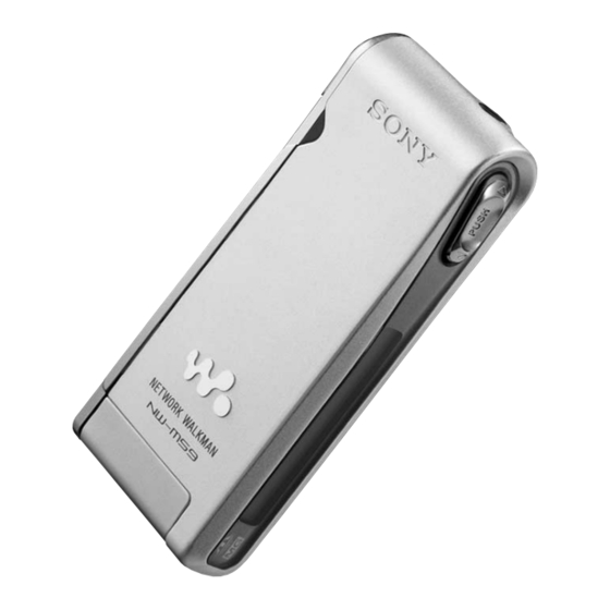
PORTABLE MEMORY STICK AUDIO PLAYER
NW-MS9
US Model
AEP Model
UK Model
E Model
Advertisement
Table of Contents

Related Manuals for Sony NW-MS9


Summary of Contents for Sony NW-MS9
- Page 1 More than 80dB (excluding 66 kbps) Key ring (1) CD-ROM (OpenMG Jukebox installation disc) (1) Dynamic range NW-MS9 Operating Instructions (1) OpenMG Jukebox Operating Instructions (1) More than 85dB (excluding 66 kbps) Operating temperature Design and specifications are subject to change 5˚C to 35˚C (-41˚F to 95˚F)
-
Page 2: Table Of Contents
3-5. Chassis (Main) Assy ............7 of the copyright holders. • Sony is not responsible for music files that are not saved on your computer due to unsuccessful recording 3-6. “Console Unit”, “SUB Board”, “MAIN Board” .... 8 from CD or music downloading. -
Page 3: Servicing Notes
NW-MS9 SECTION 1 SERVICING NOTES • NOTE FOR REPLACING THE EEPROM (IC6002) In case of replacing the EEPROM (IC6002) when repairing this set, it is necessary to write the setting for destination. When replacing the EEPROM (IC6002), write the setting for destination, referring to “4. -
Page 4: General
NW-MS9 SECTION 2 This section is extracted from instruction manual. GENERAL (rear) Looking at the controls Network Walkman (front) 6 i (Headphones/earphones) jack (page 11) 7 Hole for attaching the key ring or strap (The strap is not supplied) 8 HOLD switch (page 16) 9 MEGA BASS/AVLS button (page 14) 0 VOLUME +/–... -
Page 5: Disassembly
NW-MS9 SECTION 3 DISASSEMBLY • This set can be disassembled in the order shown below. 3-1. DISASSEMBLY FLOW 3-2. Case block assy 3-3. Case 3-4. Guide (LED) 3-5. Chassis (main) assy 3-6. “Console unit”, 3-7. Console assy 3-8. Console board “Sub board”... -
Page 6: Case
NW-MS9 3-3. CASE console unit knob (hold) console unit switch knob (hold) 1 Inclining the console unit in the direction of arrow, remove the switch from the knob (hold). 3 case 2 Take off the console flexible board from the case. -
Page 7: Guide (Led)
NW-MS9 3-4. GUIDE (LED) 7 Remove the guide (LED) in the direction of arrow B . 5 two claws 6 cover (side) × 4 screw (M1.4 3 label 1 Open the lid (PC) in the direction of arrow A . -
Page 8: Console Unit", "Sub Board", "Main Board
NW-MS9 3-6. “CONSOLE UNIT”, “SUB BOARD”, “MAIN BOARD” 4 console unit 3 console flexible board (CN300) 1 connector (CN200) 6 MAIN board 5 SUB board 3-7. CONSOLE ASSY 5 console assy 3 Remove the CONSOLE board in the direction of arrow A . -
Page 9: Console Board
NW-MS9 3-8. CONSOLE BOARD 1 window (LCD) 2 button (play) 3 CONSOLE board... -
Page 10: Test Mode
NW-MS9 SECTION 4 TEST MODE [Preparation] Checking consumed electric current is one of the items to check. Connect an ammeter before setting the test mode. (Refer to the following figure) regulated dc ammeter power supply – – 1.23Vdc – MAIN BOARD (Conductor Side) –... - Page 11 NW-MS9 [Flow Chart of Operations in the Test Mode] Enter the test mode 1. ROM/RAM Self-check 2. Display of version and destination [VOLUME+] [VOLUME--] [DISPLAY] 3. Writing destination 8. Sleep mode (Checking voltage and (Checking consumed electric current) consumed electric current)
- Page 12 NW-MS9 3. Writing Destination (Checking Voltage and Consumed Electric Current) After entering this mode, display of version and destination blinks. (The LCD back light turns off) 3-1. Checking voltage and consumed electric current Note: Perform checking voltage and consumed electric current with the LCD back light off.
- Page 13 NW-MS9 6. USB Self-check The indication is displayed as below after entering this mode. display 3.USB > This mode is not used in servicing. [MENU] Press the key to go to the next RTC self-check. 7. RTC Self-check The indication is displayed as below after entering this mode.
- Page 14 NW-MS9 MEMO...
-
Page 15: Diagrams
NW-MS9 SECTION 5 DIAGRAMS 5-1. BLOCK DIAGRAM – MAIN Section – DSP, MAGIC GATE CORE, MEMORY STICK INTERFACE, CN6000 D/A CONVERTER HEADPHONE AMP USB INTERFACE MEMORY STICK IC3100 IC3200 IC8000 MS DIO SDATA PCMO J3301 ∆∑ OUTB R-CH IN B... -
Page 16: Block Diagram -Display/Power Supply Section
NW-MS9 5-2. BLOCK DIAGRAM – DISPLAY/POWER SUPPLY Section – XRST2 (Page 15) SAM RST LEVEL SHIFT SWITCHING Q7502, 7503 IC7500 (2/4) +1.9V REGULATOR (Page 15) IC9006 DC/DC CONVERTER B+ SWITCH D9002, L9001, Q9006, 9007 Q9008 SAM RST RESET SIGNAL D9015... -
Page 17: Note For Printed Wirinig Boards And Schematic Diagrams
NW-MS9 5-3. NOTE FOR PRINTED WIRING BOARDS AND SCHEMATIC DIAGRAMS Note on Printed Wiring Boards: Note on Schematic Diagram: • All capacitors are in µF unless otherwise noted. pF: µµF • X : parts extracted from the component side. • Y : parts extracted from the conductor side. - Page 18 NW-MS9 • Waveforms – MAIN board – – SUB board – 1 IC7001 <zb/ (XTO) qa IC3100 1 (MCLK) 6 IC9005 wk, es (L1) 2 V/DIV, 2 µs/DIV 500 mV/DIV, 20 ns/DIV 1 V/DIV, 50 ns/DIV 2.6 Vp-p 2.8 Vp-p 1.7 Vp-p...
-
Page 19: Printed Wiring Boards -Main Section
NW-MS9 5-4. PRINTED WIRING BOARDS – MAIN Section – :Uses unleaded solder. • Semiconductor LED6000 CN6002 (FRONT VIEW) Location MAIN BOARD (COMPONENT SIDE) Ref. No. Location D1001 D6000 H-11 LED6000 (ACCESS INDICATOR) D9001 D-12 R6022 R6591 D9002 E-11 Q6007 IC6002... -
Page 20: Schematic Diagram -Main Section (1/4)
NW-MS9 5-5. SCHEMATIC DIAGRAM – MAIN Section (1/4) – • See page 18 for Waveforms. • See page 27 for IC Block Diagram. (Page 23) (Page (Page (Page... -
Page 21: Schematic Diagram -Main Section (2/4)
NW-MS9 5-6. SCHEMATIC DIAGRAM – MAIN Section (2/4) – • See page 27 for IC Block Diagrams. (Page 20) (Page 22) (Page 23) -
Page 22: Schematic Diagram -Main Section (3/4)
NW-MS9 5-7. SCHEMATIC DIAGRAM – MAIN Section (3/4) – • • See page 18 for Waveform. See page 28 for IC Block Diagrams. (Page 23) (Page 21) (Page 20) -
Page 23: Schematic Diagram -Main Section (4/4)
NW-MS9 5-8. SCHEMATIC DIAGRAM – MAIN Section (4/4) – • • See page 18 for Waveforms. See page 29 for IC Block Diagrams. (Page 20) (Page 21) (Page 22) -
Page 24: Schematic Diagram -Sub Section (1/2)
NW-MS9 5-9. SCHEMATIC DIAGRAM – SUB Section (1/2) – (Page 25) (Page 20) -
Page 25: Schematic Diagram -Sub Section (2/2)
NW-MS9 5-10. SCHEMATIC DIAGRAM – SUB Section (2/2) – • • See page 18 for Waveforms. See page 30 for IC Block Diagrams. (Page 24) -
Page 26: Printed Wiring Board -Sub Section
NW-MS9 5-11. PRINTED WIRING BOARD – SUB Section – :Uses unleaded solder. SUB BOARD (COMPONENT SIDE) D3101 R1001 D3201 CN300 C1000 1-680-376- C3314 R3104 R3204 (12) CN200 C3310 Q3301 R3201 C3201 C3101 R3304 R3101 MAIN BOARD (Page 19) CONSOLE CN100... - Page 27 NW-MS9 • IC Block Diagrams – MAIN Board – IC1001 RV5C348A-E2 ALARM W REGISTER VOLTAGE COMPARATOR W (WEEK,MIN,HOUR) DETECT 32KHz 32K OUT OUTPUT ALARM D REGISTER CONTROL COMPARATOR D (MIN,HOUR) OSC IN TIME COUNTER DIVIDER (SEC,MIN,HOUR,WEEK,DAY,MONTH,YEAR) CORRECTION OSC OUT SCLK...
- Page 28 NW-MS9 IC5600 HY62UF16201ALLF-85I IC5800 SN74LV139APWR SELECT DATA OUTPUTS 32 31 30 29 28 27 26 25 I/O4 14 13 12 11 I/O5 Y0 Y1 Y2 Y3 Y0 Y1 Y2 Y3 ADDRESS ADDRESS ADDRESS BUFFER BUFFER BUFFER SELECT DATA OUTPUTS PRE DECODER...
- Page 29 NW-MS9 IC9001 XC6368A281MR IC9004 XC6365A183MR PWM/PFM RAMP WAVE PHASE VOUT CONTROLER GENERATOR, COMPENSATION ERROR AMP COMPARATOR BUFFER, EXT/ – DRIVER BUFFER, – ERROR DRIVER – COMPARATOR PHASE VREF WITH SOFT START, COMPENSATION VREF WITH RAMP WAVE PWM/PFM SOFT START, GENERATOR,...
- Page 30 NW-MS9 IC9006 XC62HR1902MR VOUT CURRENT LIMIT – OUTPUT REFERENCE CONTROL VOLTAGE – SUB Board – IC3100 AK4352VT-E2 MCLK CLOCK DIVIDER VCML ∆ Σ BLCK AOUTL MODULATOR INTERPOLATOR ∆ Σ SDATA AOUTR MODULATOR INTERPOLATOR SERIAL INPUT LRCK INTERFACE VCMR VREF DIF0...
-
Page 31: Ic Pin Function Description
NW-MS9 5-12. IC PIN FUNCTION DESCRIPTION • MAIN BOARD IC7001 CXD9534BGG (SYSTEM CONTROLLER) Pin No. Pin Name Description Two-way data bus with the flash memory (IC5000), S-RAM (IC5600) and CXD1859GA 1 to 7 D6 to D0 (IC8000) VDDIO1 — Power supply terminal (+2.8V) VSSIO1 —... - Page 32 NW-MS9 Pin No. Pin Name Description System hold off signal input from the HOLD switch of console unit WAKE1 The signal input, when switch position is changed from on to off WAKE0 System wake up signal input by any key is pressed...
- Page 33 NW-MS9 Pin No. Pin Name Description USB XDET Not used (open) VBUS XON Not used (open) VBUS INT USB connect detection signal input from the voltage detector (IC9003) USB XDREQ Not used (fixed at “L”) USB XINT Not used (fixed at “L”)
- Page 34 NW-MS9 Pin No. Pin Name Description VDDIO2 — Power supply terminal (+2.8V) VSSIO2 — Ground terminal 173 to 180 Not used (open) FRIO8 to FRIO15 VDDIO2 — Power supply terminal (+2.8V) VSSIO2 — Ground terminal 183 to 187 FRCE0 to FRCE4...
- Page 35 NW-MS9 Pin No. Pin Name Description XTRSTD Not used (open) VSSCORE — Ground terminal TDOD Not used (open) Not used (open) VDDCORE — Power supply terminal (+1.8V) 240, 241 MSEL0D, MSEL1D Not used (open) 242, 243 MSEL1, MSEL0 Not used (open) VSSIO1 —...
- Page 36 NW-MS9 • MAIN BOARD IC8000 CXD1859GA (DIGITAL SIGNAL PROCESSOR, MAGIC GATE CORE, MEMORY STICK INTERFACE, USB INTERFACE) Pin No. Pin Name Description CLKSEL2 Clock mode setting terminal Fixed at “L” in this set XTAL0 Sub system clock output terminal (22.5MHz) Not used (open)
- Page 37 NW-MS9 Pin No. Pin Name Description Two-way data bus with the flash memory (IC5000), S-RAM (IC5600) and system controller 54 to 56 DB12 to DB14 (IC7001) VSS6 — Ground terminal Two-way data bus with the flash memory (IC5000), S-RAM (IC5600) and system controller...
- Page 38 NW-MS9 Pin No. Pin Name Description TKTINT Not used (open) Mode setting terminal Fixed at “H” in this set VDE7 — Power supply terminal (+2.8V) 114, 115 MD1, MD2 Mode setting terminal Fixed at “H” in this set TRST Not used (fixed at “L”) VSS13 —...
-
Page 39: Exploded Views
NW-MS9 SECTION 6 EXPLODED VIEWS NOTE: • -XX and -X mean standardized parts, so they • Items marked “*” are not stocked since they may have some difference from the original are seldom required for routine service. Some one. delay should be anticipated when ordering •... -
Page 40: Main Board Section
NW-MS9 6-2. MAIN BOARD SECTION not supplied not supplied not supplied Ref. No. Part No. Description Remark Ref. No. Part No. Description Remark 3-225-318-01 SHEET (BATTERY), INSULATING 3-348-998-51 SCREW (M1.4X3.5), TAPPING, PAN 3-225-317-01 CHASSIS (MAIN) 1-680-378-11 SWITCH FLEXIBLE BOARD * 53... -
Page 41: Electrical Parts List
NW-MS9 SECTION 7 ELECTRICAL PARTS LIST MAIN NOTE: • Due to standardization, replacements in the • Items marked “*” are not stocked since they The components identified by parts list may be different from the parts speci- are seldom required for routine service. - Page 42 NW-MS9 MAIN Ref. No. Part No. Description Remark Ref. No. Part No. Description Remark D9001 8-719-076-80 DIODE SBS004 D9002 8-719-072-27 DIODE MA2Z748001S0 < TRANSISTOR > D9004 8-719-046-85 DIODE MA2S728 Q6000 8-729-928-81 TRANSISTOR DTC144EE D9005 8-719-072-27 DIODE MA2Z748001S0 Q6001 8-759-593-78 FET...
- Page 43 NW-MS9 MAIN Ref. No. Part No. Description Remark Ref. No. Part No. Description Remark R7123 1-218-985-11 RES-CHIP 470K 1/16W R9502 1-218-965-11 RES-CHIP 1/16W R7126 1-218-985-11 RES-CHIP 470K 1/16W < VIBRATOR > R7127 1-218-985-11 RES-CHIP 470K 1/16W R7154 1-218-985-11 RES-CHIP 470K...
- Page 44 NW-MS9 Ref. No. Part No. Description Remark Ref. No. Part No. Description Remark < FERRITE BEAD > ACCESSORIES & PACKING MATERIALS ******************************** FB3101 1-469-084-21 FERRITE 1mH 0 101 FB3201 1-469-084-21 FERRITE 1mH 1-476-726-11 CHARGER, BATTERY (BC-MS9AE) (AEP, Korean) < IC >...
- Page 45 NW-MS9 BATTERY CHARGER (1) BC-9HG2 RECHARGEABLE BATTERY (1) USB CABLE (1) CARRYING POUCH (1) EARPHONES (1) RECHAGEABLE BATTERY CARRYING CASE (1) Note : Name of these illustrated parts are described as they are in the operating instructions.
- Page 46 NW-MS9 REVISION HISTORY Clicking the version allows you to jump to the revised page. Also, clicking the version at the upper right on the revised page allows you to jump to the next revised page. Ver. Date Description of Revision...