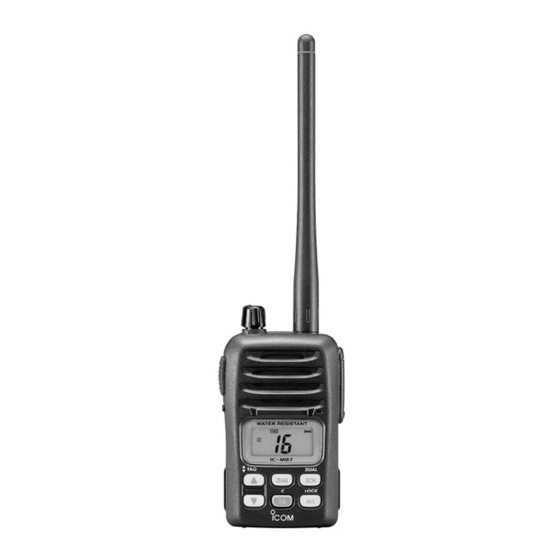
Icom IC-M87 Service Manual
Hide thumbs
Also See for IC-M87:
- Instruction manual (48 pages) ,
- Instruction manual (13 pages) ,
- Instruction manual (10 pages)
Table of Contents
Advertisement
Quick Links
GUIDE FOR CD
1) COMPOSION
IC-M87_ATEX
2) DESCRIPTION
M87_ATEX.pdf
The service manual for IC-M87 (ATEX version) including all service information in this CD. This fi le is mainly used for viewing on
the computer display and checking page order to make printed service manual. Or when you want to fi nd a component, you can
fi nd very fast using "FIND" function (except Board Layouts).
A3format.pdf
Consists of A3 format pages (Board layouts, Mechanical parts and disassembly, and etc.). This fi le is used for printing out A3
format pages.
A4format.pdf
Consists of A4 format pages (Circuit description, Adjustment procedures, Parts list, and etc.). This fi le is used for printing out A4
format pages.
Instruction.pdf
The instruction manual for IC-M87 (ATEX version). The contents of this fi le is exactly same as supplied instruction manual with
product and consists of all A4 format pages. If you have A4 format printer, you can print and make brand new instruction manual
any time you want. This fi le is also very helpful when you want to change or set product setting condition for adjustment or else.
M87_ATEX.pdf
FYC
Installer
README.txt
1
A3format.pdf
A4format.pdf
Instruction.pdf
ar505eng.exe
Advertisement
Table of Contents

Related Manuals for Icom IC-M87


Summary of Contents for Icom IC-M87
- Page 1 M87_ATEX.pdf The service manual for IC-M87 (ATEX version) including all service information in this CD. This fi le is mainly used for viewing on the computer display and checking page order to make printed service manual. Or when you want to fi nd a component, you can fi...
- Page 2 Reader yet. ========================================================================================= Icom, Icom Inc. and Icom logo are registered trademarks of Icom Incorporated (Japan) in the United states, the United Kingdom, Germany, France, Spain, Russia and/or other countries. Acrobat Reader Copyright © 1987-2002 Adobe Systems Incorporated. All rights reserved.
- Page 3 ��� ������ ����������� iC-m87 ����� �������� ������������ ���� ����...
- Page 4 ������� ��� ������ ��� ����������� �� �� ���� �������� ������ ������ ��� ���� �� ��������� �� �� ���� �������� ������ ������������ ���� �������� ���� �� �������� �� ���� ��������� ����� ���������� ��� �������� �������� ���� ������ �� �� �������� ��������� ������������...
-
Page 5: Table Of Contents
TABLE OF CONTENTS SECTION 1 SPECIFICATIONS SECTION 2 INSIDE VIEWS SECTION 3 DISASSEMBLY INSTRUCTIONS SECTION 4 CIRCUIT DESCRIPTION 4 - 1 RECEIVER CIRCUITS ....................4 - 1 4 - 2 TRANSMITTER CIRCUITS .................... 4 - 2 4 - 3 PLL CIRCUITS ........................ 4 - 3 4 - 4 POWER SUPPLY CIRCUITS .................. - Page 6 SECTION 1 SPECIFICATIONS M GENERAL • Frequency coverage : TX: 156.000–161.450 MHz, RX: 156.000–163.425 MHz [MARINE] TX/RX: 146.000–174.000 MHz [PMR] • Number of free channels : 22 channels • Type of emission : 16K0G3E (Wide; 25 kHz) [MARINE] for ATIS 16K0F3E (Wide;...
- Page 7 M VHF MARINE CHANNEL LIST Channel No. Frequency (MHz) Channel No. Frequency (MHz) Channel No. Frequency (MHz) Transmit Receive Transmit Receive Transmit Receive 156.050 160.650 157.100 161.700 156.725 156.725 156.050 156.050 157.100 157.100 156.775 156.775 156.100 160.700 157.150 161.750 156.825 156.825 156.150 160.750...
- Page 8 SECTION 2 INSIDE VIEWS • LOGIC UNIT Bottom view *: Located under side of this point. AF mute circuit Q441* : 2SC4116 Q442* : CPH3403 Q443 : CPH3403 IN/EXT microphone switch Q444 : DTC144EU (Q461, Q462: UN911H) EEPROM Microphone amplifier (IC591*: HN58X2416TI) (IC471: NJM2904V) AF mute...
-
Page 9: Disassembly Instructions
SECTION 3 DISASSEMBLY INSTRUCTIONS 1. Removing the chassis panel q Remove a nut A. w Unscrew 2 screws B (2 × 8 mm, black) and 3 screws C (2 × 4 mm, black) from the chassis. e Take off the chassis in the direction of the arrow. NOTE: * Tighten the screws in order of a number (q–y) when assembling. -
Page 10: Circuit Description
SECTION 4 CIRCUIT DESCRIPTION 4-1 RECEIVER CIRCUITS 4-1-3 1ST MIXER AND 1ST IF CIRCUITS (MAIN UNIT) 4-1-1 ANTENNA SWITCHING CIRCUIT (MAIN UNIT) The 1st mixer circuit converts the received signal into the The antenna switching circuit functions as a low-pass fi lter fi... -
Page 11: Transmitter Circuits
The 2nd IF signal from the 2nd mixer section (IC231, pin 3) 4-2 TRANSMITTER CIRCUITS passes through the ceramic fi lter (Wide: FI231 only, Narrow: 4-2-1 MICROPHONE AMPLIFIER CIRCUIT both FI231 and FI232) to remove unwanted heterodyned fre- (LOGIC UNIT) quencies. -
Page 12: Pll Circuits
4-3 PLL CIRCUITS The amplified signal is passed through the low-pass filter 4-3-1 PLL CIRCUIT (MAIN UNIT) (L121, L122, C121, C122), power detector (D121), antenna A PLL circuit provides stable oscillation of the transmit fre- switching circuit (D131) and another low-pass filter (L131, quency and receive 1st LO frequency. -
Page 13: Power Supply Circuits
4-3-2 VCO CIRCUITS (MAIN UNIT) 4-5 PORT ALLOCATIONS The VCO circuits contain a separate RX VCO (Q41, D31– 4-5-1 CPU (LOGIC UNIT; IC166) D34) and TX VCO (Q51, D35–D38). The oscillated signal is Port amplifi ed at the buffer amplifi ers (Q61, Q62) and is then ap- Description number name... - Page 14 4-5-2 EXPANDER (MAIN UNIT; IC341) CPU (continued) Port Port Description Description number name number name Outputs the internal speaker control Outputs the scrambler switch (IC281, signal. pin 3) control signal. SRXMS ISPMS Low : While the scrambler function High : While connecting the external OFF.
-
Page 15: Adjustment Procedures
SECTION 5 ADJUSTMENT PROCEDURES 5-1 PREPARATION When adjusting IC-M87, JIG cable (see illustration on page 5-2), RS-232C cable and optional CS-M88 ADJ ADJUSTMENT are required. (Rev. 1.0 or later) SOFTWARE M REQUIRED TEST EQUIPMENT EQUIPMENT GRADE AND RANGE EQUIPMENT GRADE AND RANGE Output voltage : 7.2 V DC... - Page 16 • CONNECTION Standard signal generator to the antenna connector 0.1 µV to 32 mV (–127 dBm to –17 dBm) Attenuator deviation meter 20 dB or 30 dB CAUTION! DO NOT transmit while RF power meter 0.1–10 W/50 Ω SSG is connected to the antenna connector.
- Page 17 • SCREEN DISPLAY EXAMPLE CS-M88 ADJ Rev.1.0 File Option COM 1: OPEN Connect Reload (F5) Disp para [A / D] [D / A] BATT : 120 : 78h : 7.53 V FRQCON : 127 : 7Fh : 2.49 V NOIS 59 : 3Bh : 1.16 V T1/POW : 92 : 5Ch :...
- Page 18 5-2 SOFTWARE ADJUSTMENTS • Select the adjustment item with [↑] / [↓] keys, then set specifi ed value or condition with [←] / [→] keys on the connected com- puter keyboard. MEASUREMENT ADJUSTMENT ADJUSTMENT CONDITION VALUE UNIT LOCATION P L L L O C K 1 •...
- Page 19 • MAIN UNIT TOP VIEW PLL lock voltage check point 5 - 5...
-
Page 20: Software Adjustment
SOFTWARE ADJUSTMENTS (Continue) • Select the adjustment item with [↑] / [↓] keys, then set specifi ed value or condition with [←] / [→] keys on the connected com- puter keyboard. MEASUREMENT ADJUSTMENT ADJUSTMENT CONDITION VALUE UNIT LOCATION NOTE: Adjust all the adjustment items as follows throughly in sequence. Side •... -
Page 21: Parts List
SECTION 6 PARTS LIST [LOGIC UNIT] [LOGIC UNIT] ORDER ORDER DESCRIPTION DESCRIPTION LOCATION LOCATION IC421 1110001811 S.IC TA7368FG (5, ER) 24.8/41.8 R494 7030003680 S.RES ERJ3GEYJ 104 V (100 kΩ) 11.8/3.9 IC471 1110003800 S.IC NJM2904V-TE1 46.2/7.1 R495 7030003520 S.RES ERJ3GEYJ 472 V (4.7 kΩ) 13.1/5.6 IC481 1130007301... -
Page 22: Main Unit
[LOGIC UNIT] [MAIN UNIT] ORDER ORDER DESCRIPTION DESCRIPTION LOCATION LOCATION C472 4550007200 S.TAN F930J476MBABMA 33.3/7.2 1140005991 S.IC MB15A02PFV1-G-BND-ER 34/35 C473 4030006900 S.CER C1608 JB 1H 103K-T 45/4.4 IC141 1110002751 S.IC TA75S01F (TE85R, F) 72.8/22.6 C481 4030006900 S.CER C1608 JB 1H 103K-T 24.8/11 IC231 1110003201... - Page 23 [MAIN UNIT] [MAIN UNIT] ORDER ORDER DESCRIPTION DESCRIPTION LOCATION LOCATION ERJ3GEYJ 100 V (10 Ω) 6200008390 S.COL 0.25-1.9-9TL 44.1/24.7 R112 7030003200 S.RES 66.9/24.7 6200006981 S.COL ELJRE R10GFA 48.1/20.6 R113 7030003520 S.RES ERJ3GEYJ 472 V (4.7 kΩ) 68.4/24.8 6200006981 S.COL ELJRE R10GFA 46.1/19.4 R114 7030003680...
- Page 24 [MAIN UNIT] [MAIN UNIT] ORDER ORDER DESCRIPTION DESCRIPTION LOCATION LOCATION R283 7030003680 S.RES ERJ3GEYJ 104 V (100 kΩ) 22.1/22 4030007100 S.CER C1608 CH 1H 560J-T 35.8/23.2 R284 7030003680 S.RES ERJ3GEYJ 104 V (100 kΩ) 22/16.8 4030007020 S.CER C1608 CH 1H 120J-T 45/27.7 R291 7030003660...
- Page 25 [MAIN UNIT] [VR UNIT] ORDER ORDER DESCRIPTION DESCRIPTION LOCATION LOCATION C231 4030006860 S.CER C1608 JB 1H 102K-T 15.5/8.2 R801 7210003130 TP76N97N-13F-10KA-2497 C232 4030007130 S.CER C1608 CH 1H 101J-T 20.1/10.9 C233 4030011600 S.CER C1608 JB 1E 104K-T 9.8/8.5 C234 4030011600 S.CER C1608 JB 1E 104K-T 9.8/13.7 C801...
- Page 26 SECTION 7 MECHANICAL PARTS AND DISASSEMBLY [CHASSIS PARTS] [LOGIC UNIT] REF. NO. ORDER NO. DESCRIPTION QTY. REF. NO. ORDER NO. DESCRIPTION QTY. MC461 7700002630 Microphone SKB-2246T-C33 6910014700 2600 ANT connector 7120000470 Jumper ERDS2T0 MP441 6910014760 S. plate OG-503040 7120000470 Jumper ERDS2T0 MP451 6910014760 S.
- Page 27 ���� � ��� ��� ���� ��� ���� � ��� ��� ����� ���� � ���� ��� ���� ��� ���� ��� ������� ������ ���� � ���� ���� ��� ��� ��� ��� ���� ��� ��� ���������� ���� ���� ���� ��� ����� ���� ��� ��...
- Page 28 CONTACT SPRING ASSEMBLY INSTRUCTION [1] PREPARING TWO SHORT LEADS q Cut the W1 (CHASSIS). w Bend the leads according to the dimensions below. 4.0–4.5 mm W1(CHASSIS) 3.5–4.0 mm [2] SOLDERING SHORT LEADS w Solder the short leads. q Cut off the area as below.
- Page 29 • BC-152 CHARGER PARTS LIST ELECTRICAL PARTS ACCESSORY PARTS ORDER NO. DESCRIPTION ORDER NO. DESCRIPTION LOCATION LOCATION REF. NO. ORDER NO. DESCRIPTION QTY. 1180000970 S.IC AN78L05M-(E1) 48.2/58.9 6510024940 CNR HEC2305-016250 Screw.5 × 30 SUS 8810001470 1190001180 S.IC MM1332BFBE 23.7/24.6 DS1 5040003020 LED SEL2410G 1110005961 S.IC S-80833CNMC-B8S-T2G...
- Page 30 SECTION 8 SEMI-CONDUCTOR INFORMATION 8 - 1 TRANSISTORS AND FETS 8 - 2 DIODES • IC-M87 • IC-M87 ������� ��� ���������� ������� ���� � ������� ����� ��������� ��������� ������ ������ ������ �������� ���������� �������� ��� �������� ���� �������� ��� �������� ������...
- Page 31 SECTION 9 BOARD LAYOUTS The combination of this page and the next page shows the unit layout in the same configuration as the actual 9-1 MAIN UNIT P.C. Board. • TOP VIEW �� ����� ���� ���� �� ��� ��� �� �� ���� �����...
- Page 32 MAIN UNIT The combination of this page and the previous page • BOTTOM VIEW shows the unit layout in the same configuration as the actual P.C. Board. �� �� �� �� �� �� �� � � �� �� �� �� ��...
- Page 33 9-2 LOGIC UNIT The combination of this page and next page shows the unit layout in the same configuration as the actual P.C. • TOP VIEW Board. Horizontal 9 - 3...
-
Page 34: Logic Unit
LOGIC UNIT Horizontal • BOTTOM VIEW CP442 VOLIN BTYPE V5VS R5VS CP441 T5VS AFOUT MICO SMICO W/NS TEMPV LOINV J411 CDECV MAIN J401 UNLKI UNIT MODIN J351 CDTENC VSSTBO EXSTBO DASTBO to VR UNIT PLSTBO SDATAO SCLKO EXOEO WDECV RSSIV NOISV TDETV BEEPO... -
Page 35: Charger Unit
9-3 CHARGER UNIT (BC-152) • TOP VIEW �� �� �� �� �� �� �� �� �� �� �� �� � � � � �� �� �� �� �� �� �� �� �� �� �� �� �� ���������� 9-5 CONNECTOR UNIT 9-4 VR UNIT •... -
Page 36: Connector Unit
CHARGER UNIT (BC-152) • BOTTOM VIEW �� �� �� �� �� �� �� �� �� �� �� �� � � �� �� �� �� �� �� �� �� �� �� �� �� �� � � ���������� CONNECTOR UNIT • BOTTOM VIEW VR UNIT ���... -
Page 37: Block Diagram
SECTION 10 BLOCK DIAGRAM ������ ���� ������ ��� ������ �������� ��� ��� ���� ���� ������� ����� ���� ���� ���� ����� ����� ������� ���� ������� ���� ���� ������� �������� �������� ��� ������� ��� ������ ���� ������� ���� ������� ������� ������� ����� ���... - Page 38 SECTION 11 VOLTAGE DIAGRAM ��� ��� ��� ��� ��� ��� ��� ������ ��� ��� ��� ����� � ��� ��� � ���� ��� ���� ��� �� ����� � � ��� ��� ��� �� ��� �� �� �� ��� ���� ����� ����� �...
- Page 39 ��� ��� ��� ��� ��� ��� ��� ��� ���� ���� ��� ����� ��� ��� ��� ���� ��� ��� ����� �� ��� ��� ����� ��� ����� ��� ��� ��� ���� ���� ���� ������� ��� ���� ���� ��� ��� ����� ��� ���� ����...
- Page 40 ����� ����� ����� ����� ����� ����� ���� ���������� ����� ���� ���� ����� ���� �� ��� ��� ��� ��� � ��� � ����� ����� ����� ����� � ���������� ��������� ���� ���� ��� � ��� ��� ����� �� ���� ��� ����� ����� �����...
- Page 41 ������� ����������� ���������� ����� ��������� ����� ����� � ��� ���� ���� ���� ��� � ��� ���� ���� ���� ��� � �������������������������������������� ���������� ������������� ������������� ��������� ���� ����� ������ ����� ��������� �� ������ ������ ������������� ���� ���� ������� ����������� ������� ����� � �� ����� �������� ���...
- Page 42 ������������ ������� ����������� ���������� ����� ��������� ����� � ���� ���� ����...