Table of Contents
Advertisement
Nov. 2015
Table of Contents
Cautionary Notes ..............................................................2
Specifications .....................................................................3
Location of Controls .........................................................4
Exploded View (Cabinet).................................................5
Plain View (Cabinet).........................................................6
Plain View (Cabinet) Parts List .......................................7
Exploded View (Chassis) .................................................8
Exploded View (Chassis) Parts List................................9
Plain View (Chassis) .......................................................10
Important Notes When Binding Wiring ......................11
Wiring Diagram/Block Diagram..................................12
Parts List ...........................................................................14
Copyright © 2015 Roland Corporation
All rights reserved. No part of this publication may be reproduced in any form without the written permission
of Roland Corporation.
Verifying the Version......................................................16
Test Mode .........................................................................16
Circuit Diagram (Main Board: 1/4)..............................20
Circuit Diagram (Main Board: 2/4)..............................22
Circuit Diagram (Main Board: 3/4)..............................24
Circuit Diagram (Main Board: 4/4)..............................26
Circuit Diagram (Jack Board) ........................................28
Circuit Diagram (Volume Board) .................................30
Circuit Diagram (PS Board) ...........................................31
Circuit Diagram (Inlet Board) .......................................31
17057004E0
SERVICE NOTES
Issued by RJA
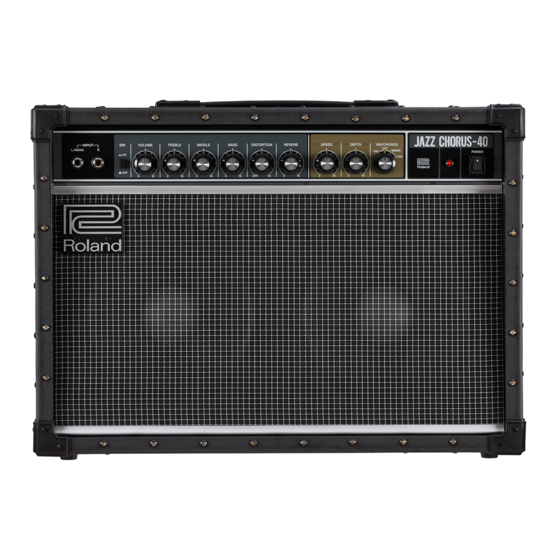
JC-40
CC-KWS
Advertisement
Table of Contents

Related Manuals for Roland JC-40


Summary of Contents for Roland JC-40
-
Page 1: Table Of Contents
Circuit Diagram (PS Board) ...........31 Wiring Diagram/Block Diagram........12 Circuit Diagram (Inlet Board) ........31 Parts List ................14 Copyright © 2015 Roland Corporation All rights reserved. No part of this publication may be reproduced in any form without the written permission of Roland Corporation. 17057004E0... -
Page 2: Cautionary Notes
• Because reissuance is restricted. • Because the part is made to order (at current market price). • Because it is carried in electronic data on the Roland web site. • Because it is a package or an accessory irrelevant to the function maintenance of the main body. -
Page 3: Specifications
* 0 dBu = 0.775 Vrms Controls * Printed matters will not be supplied after the end of the production. Then, download the electronic file from the Roland web site. POWER switch BRI (Bright) Switch * In the interest of product improvement, the specifications and/or appearance of VOLUME knob this unit are subject to change without prior notice. -
Page 4: Location Of Controls
Nov. 2015 JC-40 Location of Controls fig.panel.eps Part Code Part Name Description Q’ty 02897801 SEESAW SWITCH SDDJE13200 94V-0 5100046595 POWER SW ESCUTCHEON 5100046598 POWER SW CUSHION 5100048310 L-7113-CW914(S) 5100046599 LED SPACER LEH5-6T 5100046591 LED ESCUTCHEON 22485314 JC-KNOB 248-314(22485314R0) 5100042592 SWITCH S171EV114GFS2AN17 * This unit includes the following parts. -
Page 5: Exploded View (Cabinet)
Nov. 2015 JC-40 Exploded View (Cabinet) fig.bunkaizu-cabinet.eps Refer to Chassis Part Code Part Name Description Q’ty 5100042788 CABINET ASSY W/O SPEAKER * This unit includes the following parts. ******** CABINET ******** NET BOARD ASSY 22510402 BADGE G.AMP 61 22310207 HANDLE (H40) -
Page 6: Plain View (Cabinet)
Nov. 2015 JC-40 Plain View (Cabinet) fig.bunkaizu-cabinet-H.eps View 1 View 2 View 3 View 4 View 5 View 6 View 7... -
Page 7: Plain View (Cabinet) Parts List
Nov. 2015 JC-40 Plain View (Cabinet) Parts List View 1 Part Code Part Name Description Q’ty 40010489 SCREW M5X30 OVAL FE BZC 40010601 SCREW M5X35 ORIGINAL TRUSS MACHINE FE BZC View 2 Part Code Part Name Description Q’ty 5100046058 SCREW 3X14... -
Page 8: Exploded View (Chassis)
Nov. 2015 JC-40 Exploded View (Chassis) fig.bunkaizu-chassis.eps... -
Page 9: Exploded View (Chassis) Parts List
Nov. 2015 JC-40 Exploded View (Chassis) Parts List Part Code Part Name Description Q’ty 00125612 KEYTOP (BLK/GRY) 22485314 JC-KNOB 248-314(22485314R0) 5100046591 LED ESCUTCHEON 5100046595 POWER SW ESCUTCHEON 5100046598 POWER SW CUSHION 02897801 SEESAW SWITCH SDDJE13200 94V-0 5100046042 CHASSIS 5100039123 POWER AMP... -
Page 10: Plain View (Chassis)
Nov. 2015 JC-40 Plain View (Chassis) fig.bunkaizu-chassis-H.eps View 8 View 9 View 8 Part Code Part Name Description Q’ty 40012945 SCREW M3X6 PAN MACHINE W/SW+PW BZC 40011112 SCREW 3X10 BINDING TAPTITE B BZC View 9 Part Code Part Name Description Q’ty... -
Page 11: Important Notes When Binding Wiring
Nov. 2015 JC-40 Important Notes When Binding Wiring Keep away the wirings shown in the figure below from resistor and diode. fig.wiring-clamp-1.eps Pass the primary wiring under the transformer so that the wiring does not touch the tip of the screw securing from the side. -
Page 12: Wiring Diagram/Block Diagram
Nov. 2015 JC-40 Wiring Diagram/Block Diagram fig.wiring-block.eps@L JACK BOARD (DIGITAL PART) LOOP CHORUS DISTORTION REVERB VIBRATO SPEED DEPTH VIB/CHORUS VOLUME BOARD JK800 JK802 JK801 SW800 VR500 VR501 SW500 VOLUME TREBLE MIDDLE BASS DISTORTION REVERB L/MONO IC30 IC18 INPUT IC31 IC13... - Page 13 Nov. 2015 JC-40 fig.wiring-block.eps@R INLET BOARD POWER LED POWER SWITCH LED600 JK700 PS BOARD Primary side POWER TRANSFORMER Secondary side Power Amplifier IC23 Left ORANGE BLACK Built-in Speaker BROWN 4 ohms Right Power Amplifier IC10 IC24 L/MONO JK803 LINE OUT...
-
Page 14: Parts List
• Reissuance is restricted. only listed parts for replacement. • It is carried in electronic data on the Roland web site. • It is supplied as an assembled part • The part is made to order (at current market price). - Page 15 Nov. 2015 JC-40 WIRING, CABLE 5100046171 WIRING W4 (1672#22-BLK) 5100046177 WIRING W5 (1015#22-RED) 5100046178 WIRING W6 (1015#22-BLK) 5100046179 WIRING W7 (1015#22-ORG) 5100046188 WIRING W8 (1015#22-BRN) 5100047043 WIRING W10 (1672#18-BLK/WHT) 5100033985 WIRING 5100046167 WIRING 1007#28 15X260-PHR-SAN-F 5100046170 WIRING 1007#28 2X230-PHR-SAN-F 5100046168...
-
Page 16: Verifying The Version
Nov. 2015 JC-40 Verifying the Version Verifying the Version The LED lights up to indicate the version as shown in the table below. Perform verification in the test mode of the next section. Version Flashing LED (repeats) 1.00 1 long flash Test Mode 1.01... - Page 17 Nov. 2015 JC-40 Input/Output Check Disconnect the speaker wiring from the L and R speaker terminals. * If the speakers are connected, when the VIB/CHORUS knob is set to VIB on the next step, sound is produced at high volume.
-
Page 18: Circuit Board (Main, Jack, Volume, Ps, Inlet Board)
Nov. 2015 JC-40 Circuit Board (Main, Jack, Volume, PS, Inlet Board) fig.b-main-1.eps... - Page 19 Nov. 2015 JC-40 fig.b-main-2.eps...
-
Page 20: Circuit Diagram (Main Board: 1/4)
Nov. 2015 JC-40 Circuit Diagram (Main Board: 1/4) fig.d-main-1.eps@L D+3.3V FOR UPDATE R129 WP_EEPROM_PROG R0923NOCH1B103FE00A1 R0923NOCH1B103FE00A1 R0923NOCH1B103FE00A1 R0923NOCH1B103FE00A1 R0923NOCH1B103FE00A1 R0923NOCH1B103FE00A1 R0923NOCH1B103FE00A1 R0923NOCH1B103FE00A1 RESET IC14 C191 TC7W08FU(TE12L.F) 100pF D+3.3V C276 C277 C278 C279 0.1uF 0.1uF 0.1uF 0.1uF VR_GND VR_GND VR_GND VR_GND... - Page 21 Nov. 2015 JC-40 fig.d-main-1.eps@R VR Layout D+3.3V D+3.3V VR2 VR3 VR4 VR5 VR6 VR7 D+3.3V LOOP_SW R225 R226 D+3.3V FC_RX R228 RESET FC_TX From JACK BOARD R227 IC14 TC7W08FU(TE12L.F) C178 C179 100pF 100pF CN14 B7B-PH-SM4-TB (LF)(SN) D+3.3V D+3.3V D+3.3V C161 0.1uF...
-
Page 22: Circuit Diagram (Main Board: 2/4)
Nov. 2015 JC-40 Circuit Diagram (Main Board: 2/4) fig.d-main-2.eps@L VCC+6V VCC+6V C282 0.1uF C283 0.1uF C285 0.1uF C286 0.1uF C293 C302 C307 0.1uF 0.1uF 0.1uF 1000pF 1000pF 1SS355 TE-17(PB FREE) VR_GND VR_GND VR_GND VR_GND C287 0.1uF C346 0.1uF 1.5k D+3.3V D+3.3V... - Page 23 Nov. 2015 JC-40 fig.d-main-2.eps@R A+8V 1SS362FV(TPL3) SP-COMMON C275 C274 2SA1586SU-GR.LF(D 2SA1586SU-GR.LF(D R192 MUTE DTA114EMT2L 1SS355 TE-17(PB FREE) R233 2SC4116SU-GR.LF(D -VCC2 A-8V -VCC2 TA114EMT2L D+3.3V R275 C294 100pF D+1.5V UnPop UnPop 1SS355 TE-17(PB FREE) 1SS355 TE-17(PB FREE) VCC+6V WQPCRH1005RD-102M-N R277 NJM2882F33-TE1...
-
Page 24: Circuit Diagram (Main Board: 3/4)
Nov. 2015 JC-40 Circuit Diagram (Main Board: 3/4) fig.d-main-3.eps@L A+5V A+8V A+8V 1SS362FV(TPL3) F (1%) 10uF A+5V D+3.3V 10uF 16V A-8V 0.1uF 10uF F (1%) 0.1uF 10uF16V INPUT L/MONO 10uF NJM2115V(TE1) 15pF 0.1uF A+5V R112 UnPop 1.5k UnPop 0.1uF 0.1uF... - Page 25 DIF0/CDTI MCLK LRCK LRCK AOUTR BICK DZFR DA0R SDTI PDN_CODEC VCOM IC31 AK4384ET-E2 C125 0.1uF JC-40 WIRING W7 (1015#22-ORG) SPEAKER RIGHT SPEAKER_MUTE MUTE 1SS355 TE-17(PB FREE) A+8V CN11 A-8V JC-40 WIRING W8 (1015#22-BRN) A+8V MUTE_FET 0.25W R250 R122 2SC4116SU-GR.LF(D CPU_MUTE_P-AMP...
-
Page 26: Circuit Diagram (Main Board: 4/4)
Nov. 2015 JC-40 Circuit Diagram (Main Board: 4/4) fig.d-main-4.eps@L C252 4700pF 22uF 16V 3.3k R206 C340 6.8k IC24 8200pF NJM4580M(TE2) 0.22uF 1200pF NJM4580M(TE2) MAIN_SIG_L 47pF UnPop 3.3k R205 3.3k C230 8200pF C101 0.022uF 100k 10uF 0.22uF UnPop 220k MUTE C272 0.056uF... - Page 27 Nov. 2015 JC-40 fig.d-main-4.eps@R A+8V IC15 NJM4556AM(TE2) 47pF MAIN_RETURN_L A+8V MAIN_RETURN_R RB706F-40 T106(PB FREE) DETECT_RETURN 150k A+8V A-8V MAIN_SEND A-8V 0.25W IC15 NJM4556AM(TE2) MUTE JACK BOARD 1500pF R223 MAIN_LINE_L MAIN_LINE_R UnPop UnPop 2SC4213-A(TE85L.F) 47pF A+8V RB706F-40 T106(PB FREE) B15B-PH-SM4-TB (LF)(SN)
-
Page 28: Circuit Diagram (Jack Board)
Nov. 2015 JC-40 Circuit Diagram (Jack Board) fig.d-jack.eps@L JACK_A+8V AG_JACK_RETURN JACK_A-8V JACK_SEND JACK_DETECT_RETURN JACK_RETURN_L AG_JACK_SEND JACK_RETURN_R MAIN BOARD AG_JACK_RETURN JACK_LINE_L JACK_LINE_R JACK_PHONES_L AG_JACK_LINE JACK_PHONES_R JACK_DETECT_PHONES CN801 PHGND_JK 5100046167 WIRING 1007#28 15X310-PHR-SAN-F(AP057 W1 C826 D801 JACK_A+8V R807 1SS362FV(TPL3) RETURN L/MONO R808... - Page 29 Nov. 2015 JC-40 fig.d-jack.eps@R R801 0.25W R802 0.25W JACK_PHONES_L RS 5 JACK_PHONES_R PHONES C805 SERIAL/PARALLEL C812 C804 C813 SW800 R800 0.01uF 0.01uF 0.01uF SV70050F-0202-10T-NN 0.01uF JK804 PJ-644C-EP SW800 C811 SW800 SV70050F-0202-10T-NN 1000pF C810 0.1uF SV70050F-0202-10T-NN 0.1uF FG_JKA PHGND_JK JACK_DETECT_PHONES FG_JKA...
-
Page 30: Circuit Diagram (Volume Board)
Nov. 2015 JC-40 Circuit Diagram (Volume Board) fig.d-volume.eps Layout SW500 SW500 S171EV114GFS2AN17 S171EV114GFS2AN17 VR500 VR501 SW500 REF+3.3V_PANELB FGND_PANELB FGND_PANELB MAIN BOARD C508 REFGND_PANELB 10uF COM1 COM2 VR_R_1 VR_R_0 SW500 CN500 S171EV114GFS2AN17 VR_BOARD_DG C501 VR_BOARD_DG 0.1uF VR_BOARD_DG FGND_PANELB REFGND_PANELB REF+3.3V_PANELB VR500... -
Page 31: Circuit Diagram (Ps Board)
Nov. 2015 JC-40 Circuit Diagram (PS Board) fig.d-PS.eps POWER SW SDDJE13200 JC-40 WIRING W4 (1672#22-BLK) 5100046171 5100046171 CN608 CN607 JC-40 WIRING W4 (1672#22-BLK) PSW1 PSW2 to TRANSFORMER CN600 B2P3-VH (LF)(SN) 7A/250V HOTSWA-PRI HOTSWB-PRI HOTPOST-PRI (HOT) FH601 FH602 CN601 C600 SIN-21T-1.8...