Advertisement
Quick Links
QQ
3 7 63 1515 0
TE
L 13942296513
www
.
PA
011912
20080527-99540
http://www.xiaoyu163.com
CONTENTS(目次)
SPECIFICATIONS(総合仕様) ................................................... 3
PANEL LAYOUT(パネルレイアウト) ..................................... 4
DIMENSIONS(寸法図) ........................................................... 4
CIRCUIT BOARD LAYOUT(ユニットレイアウト) ................. 5
DISASSEMBLY PROCEDURE(分解手順) .............................. 6
LSI PIN DESCRIPTION(LSI 端子機能表) ............................. 14
IC BLOCK DIAGRAM(IC ブロック図) .................................. 16
CIRCUIT BOARDS(シート基板図) ....................................... 17
INSPECTIONS(検査) ............................................................ 25
(アンプユニットの調整) ......................................................... 28
INITIAL SETTING(出荷時の設定) ........................................ 28
PARTS LIST
BLOCK DIAGRAM(ブロックダイアグラム)
x
ao
u163
CIRCUIT DIAGRAM(回路図)
y
i
2 9
8
SERVICE MANUAL
Q Q
3
6 7
1 3
1 5
co
.
Copyright (c) Yamaha Corporation. All rights reserved. PDF
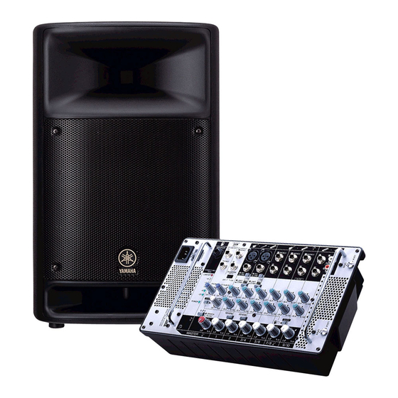
STAGEPAS 250M
9 4
2 8
Speaker
0 5
8
2 9
9 4
2 8
m
HAMAMATSU, JAPAN
9 9
9 9
Mixer
1
'08.06
Advertisement

Related Manuals for Yamaha STAGEPASS 250M


Summary of Contents for Yamaha STAGEPASS 250M
-
Page 1: Table Of Contents
IC BLOCK DIAGRAM(IC ブロック図) ........16 CIRCUIT BOARDS(シート基板図) ........17 INSPECTIONS(検査) ............25 ADJUSTMENT OF AMPLIFIER UNIT (アンプユニットの調整) ............28 INITIAL SETTING(出荷時の設定) ........28 PARTS LIST BLOCK DIAGRAM(ブロックダイアグラム) u163 CIRCUIT DIAGRAM(回路図) 011912 20080527-99540 HAMAMATSU, JAPAN Copyright (c) Yamaha Corporation. All rights reserved. PDF ’08.06... - Page 2 IMPORTANT NOTICE This manual has been provided for the use of authorized Yamaha Retailers and their service personnel. It has been assumed that basic service procedures inherent to the industry, and more specifically Yamaha Products, are already known and understood by the users, and have therefore not been restated.
- Page 3 http://www.xiaoyu163.com STAGEPAS 250M 3 7 63 1515 0 総合仕様 SPECIFICATIONS General Specifi cations 一般仕様 Maximum Output Power 最大出力 250 W (±10 %)/4 Ω @10 % THD at 1 kHz (SPEAKER) 250W( ± 10%)/4 Ω @10% THD at 1kHz (SPEAKER) 200 W/4 Ω @1 % THD at 1 kHz (SPEAKER) ≧...
-
Page 4: Panel Layout(パネルレイアウト
http://www.xiaoyu163.com STAGEPAS 250M 3 7 63 1515 0 PANEL LAYOUT(パネルレイアウト) q [AC IN] jack ([AC IN] 端子 ) !2 [PHANTOM] switch ([PHANTOM] 切り替えスイッチ ) w [POWER] switch ([POWER] スイッチ ) !3 [LIMIT/COMP] switches ([LIMIT/COMP] スイッチ ) e [SPEAKER] jack (for included speaker (500S) only) !4 Equalizer [HIGH]/[LOW] (EQ( イコライザー... -
Page 5: Circuit Board Layout(ユニットレイアウト
http://www.xiaoyu163.com STAGEPAS 250M 3 7 63 1515 0 CIRCUIT BOARD LAYOUT(ユニットレイアウト) Front view Right side view Speaker HF <Tweeter> (スピーカHF <ツィーター>) NETWORK NETWORK POWER INPUT CONTROL MOTHER JACK L 13942296513 Speaker LF <Woofer> (スピーカLF <ウーファー>) Rear view INPUT CONTROL POWER MOTHER u163 JACK... -
Page 6: Disassembly Procedure(分解手順
http://www.xiaoyu163.com STAGEPAS 250M 3 7 63 1515 0 (分解手順) DISASSEMBLY PROCEDURE Front Grille Assembly 1. フロントグリル Ass y (所要時間:約 1 分) 1-1 [180A] の ネ ジ 4 本 を 外 し て、 フ ロ ン ト グ リ ル (Time required: About 1 minute) Remove the four (4) screws marked [180A]. - Page 7 http://www.xiaoyu163.com STAGEPAS 250M 3 7 63 1515 0 Speaker LF (Woofer) Speaker HF (Tweeter) (スピーカLF(ウーファー)) (スピーカHF(ツィーター)) Wire HF (Blue) Wire HF (Yellow) Wire LF (Black) Wire LF (Red) (束線HF(青)) (束線HF(黄)) (束線LF(黒)) (束線LF(赤)) Photo 1 ( 写真 1) Photo 2 ( 写真 2) Speaker HF (Tweeter) 4. ...
- Page 8 http://www.xiaoyu163.com STAGEPAS 250M 3 7 63 1515 0 Mixer Assembly 6. ミキサー Ass y (所要時間:約 1 分) (Time required: About 1 minute) 6-1 コ イ ン ド ラ イ バ ー ま た は マ イ ナ ス ド ラ イ バ ー Rotate the two (2) straight slots on the fastener heads で、ファスナーヘッドのマイナス形溝...
- Page 9 http://www.xiaoyu163.com STAGEPAS 250M 3 7 63 1515 0 Rear Case 8. リアケース (所要時間:約 2 分) (Time required: About 2 minutes) 8-1 ミキサー Ass y を外します。 (6 項参照) Remove the mixer assembly. (See procedure 6) 8-2 [310] のネジ 8 本と [320] の特殊平座金 2 個を外し Remove the eight (8) screws marked [310] and the て、ミキサー...
- Page 10 http://www.xiaoyu163.com STAGEPAS 250M 3 7 63 1515 0 AMP Circuit Board, MOTHER Circuit 11. AMP シート、MOTHER シート Board (所要時間:約 4 分) (Time required: About 4 minutes) 11-1 Remove the mixer assembly. (See procedure 6) 11-1 ミキサー Ass y を外します。 (6 項参照) 11-2 Remove the rear case.
- Page 11 http://www.xiaoyu163.com STAGEPAS 250M 3 7 63 1515 0 INPUT Circuit Board 12. INPUT シート (所要時間:約 8 分) (Time required: About 8 minutes) 12-1 ミキサー Ass y を外します。 (6 項参照) 12-1 Remove the mixer assembly. (See procedure 6) 12-2 リアケースを外します。 (8 項参照) 12-2 Remove the rear case.
- Page 12 http://www.xiaoyu163.com STAGEPAS 250M 3 7 63 1515 0 13. CONTROL シート CONTROL Circuit Board (所要時間:約 9 分) (Time required: About 9 minutes) 13-1 ミキサー Ass y を外します。 (6 項参照) 13-1 Remove the mixer assembly. (See procedure 6) 13-2 リアケースを外します。 (8 項参照) 13-2 Remove the rear case.
- Page 13 http://www.xiaoyu163.com STAGEPAS 250M 3 7 63 1515 0 Power Switch, AC Inlet 14. 電源スイッチ、AC インレット (Time required: About 5 minutes) (所要時間:約 5 分) 14-1 Remove the mixer assembly. (See procedure 6) 14-1 ミキサー Ass y を外します。 (6 項参照) 14-2 Remove the rear case.
-
Page 14: Lsi Pin Description(Lsi 端子機能表
http://www.xiaoyu163.com STAGEPAS 250M 3 7 63 1515 0 LSI PIN DESCRIPTION(LSI 端子機能表) YMW767-VTZ (X6055A0R) CPU (SWL01B) DSP: IC1007 NAME FUNCTION NAME FUNCTION Ground Ground Input for TEST Power supply +3.3 V TESTN PLLBPN PLL bypass select External memory lower-byte enable / Port F LBN/LWRN/PF6 PLLV PLL Power supply +2.5 V... - Page 15 http://www.xiaoyu163.com STAGEPAS 250M 3 7 63 1515 0 AK5381VT (X8575A00) ADC (Analog to Digital Converter) DSP: IC1004 DAC1A: IC401 NAME FUNCTION NAME FUNCTION AINR Rch Analog input pin SDTO Audio serial data output pin AINL Lch Analog input pin LRCK Output channel clock pin CKS1 Mode select 1 pin...
-
Page 16: Ic Block Diagram(Ic ブロック図
http://www.xiaoyu163.com STAGEPAS 250M 3 7 63 1515 0 IC BLOCK DIAGRAM(IC ブロック図) FA3641N (X8570A00) PWM Control POWER: IC803 6.5 A 0.82V~0.68V 15.5V – UVLO 15.5V 5V REF 0.9mA – RTRch – – 16.5V/9V 8.5V~7.9V 0.8V IS(+)/IS(-) 3.0V – OUTPUT – –... - Page 17 http://www.xiaoyu163.com STAGEPAS 250M 3 7 63 1515 0 (シート基板図) CIRCUIT BOARDS AMP Circuit Board (4202-20) ..............24 CONTROL Circuit Board (6493-30) ............20/21 DSP Circuit Board (1054-20) ..............17 INPUT Circuit Board (6493-30)..............22 JACK Circuit Board (5255B-20) ..............24 MOTHER Circuit Board (6493-30) .............
- Page 18 http://www.xiaoyu163.com STAGEPAS 250M 3 7 63 1515 0 ● POWER Circuit Board to POWER switch AC IN to MOTHER-CN541 to CONTROL-CN1 L 13942296513 u163 Component side(部品側) 476433...
- Page 19 http://www.xiaoyu163.com STAGEPAS 250M 3 7 63 1515 0 ● POWER Circuit Board L 13942296513 u163 Pattern side(パターン側) 476433...
- Page 20 http://www.xiaoyu163.com STAGEPAS 250M 3 7 63 1515 0 ● CONTROL Circuit Board L 13942296513 to POWER-CN802 u163 Component side(部品側) 474884...
- Page 21 http://www.xiaoyu163.com STAGEPAS 250M 3 7 63 1515 0 ● CONTROL Circuit Board L 13942296513 u163 Pattern side(パターン側) 474884...
- Page 22 http://www.xiaoyu163.com STAGEPAS 250M 3 7 63 1515 0 ● INPUT Circuit Board L 13942296513 Component side(部品側) Pattern side(パターン側) u163 474884...
- Page 23 http://www.xiaoyu163.com STAGEPAS 250M 3 7 63 1515 0 ● MOTHER Circuit Board to AMP-1101 to POWER-CN804 to AMP-1100 Component side(部品側) L 13942296513 Pattern side(パターン側) SPEAKER u163 MOTHER: 474884 JACK: 475008...
- Page 24 http://www.xiaoyu163.com STAGEPAS 250M 3 7 63 1515 0 ● AMP Circuit Board to MOTHER-CN544 Pattern side(パターン側) to MOTHER-CN543 Component side(部品側) ● NETWORK Circuit Board ● JACK Circuit Board L 13942296513 to NETWORK-CN8 Component side(部品側) Component side(部品側) u163 AMP: 479246 JACK: 475008 NETWORK: 475008...
- Page 25 http://www.xiaoyu163.com STAGEPAS 250M 3 7 63 1515 0 (検査) INSPECTIONS Test Conditions (試験条件) Measuring Voitage (測定電圧) AC 100 V 50/60 Hz (J) AC 120 V 60 Hz (U) AC 230 V 50 Hz (B, E) AC 220 V 50 Hz (K, O) 4 Ω...
- Page 26 http://www.xiaoyu163.com STAGEPAS 250M 3 7 63 1515 0 ITEM INPUT CONDITIONS OUTPUT CONDITIONS NOMINAL LIMIT (項目) (入力条件) (出力条件) (標準値) (限界値) INPUT SENSITIVITY INPUT 9/10 (Each pair) STEREO SUB OUT: L, R -20 dBu -20 dBu±2 dB (入力感度) INPUT=PHONE, RCA +4 dBu OUTPUT INPUT-LEVEL=MAX.
- Page 27 http://www.xiaoyu163.com STAGEPAS 250M 3 7 63 1515 0 ITEM INPUT CONDITIONS OUTPUT CONDITIONS NOMINAL LIMIT (項目) (入力条件) (出力条件) (標準値) (限界値) SIGNAL TO NOISE RATIO INPUT SHORT SP OUT: LINK OUT R 53 dB >50 dB (信号雑音比) (入力短絡) REF: 100 W OUTPUT PLUG IN INPUT-SW=LINE (基準...
-
Page 28: Adjustment Of Amplifier Unit(アンプユニットの調整
http://www.xiaoyu163.com STAGEPAS 250M 3 7 63 1515 0 Limiter Indication (リミッタ−表示の確認) The product shall be set to 32 dBu output on SP OUT. Then, LIMITER LED(RED) should light on and all LEDs of LEVEL meter should light on. (SP OUT に 32 dBu を出力させた時、LIMITER 表示 LED(赤色)が点灯し(一瞬でも可) 、LEVEL 表示 LED が全て 点灯することを確認します。... - Page 29 http://www.xiaoyu163.com 3 7 63 1515 0 PARTS LIST CONTENTS(目次) OVERALL ASSEMBLY(総組立) ............2 MIXER ASSEMBLY(ミキサー Ass'y) ..........5 ELECTRICAL PARTS(電気部品) ..........8-26 L 13942296513 Notes : DESTINATION ABBREVIATIONS A : Australian model M : South African model B : British model O : Chinese model C : Canadian model Q : South-east Asia model...
- Page 30 http://www.xiaoyu163.com STAGEPAS 250M 3 7 63 1515 0 OVERALL ASSEMBLY(総組立) Mixer assembly: Rear cabinet unit Bracket fastner 1 assembly See page 5. (リアキャビネット部) (ブラケットファスナー1 Ass'y) (ミキサーAss'y) J,B,E,K,O models Bracket fastner 2 assembly (ブラケットファスナー2 Ass'y) B,E models only U model only Rear cabinet assembly (リアキャビネットAss'y)...
- Page 31 ク ッ シ ョ ン グ リ ル B 450793 170d WJ325400 Logo Badge ロ ゴ バ ッ ジ YAMAHA 441149 170e WJ325300 Cushion Badge ク ッ シ ョ ン バ ッ ジ 445103 170f WJ325500 Bush Nut ブ ッ シ ュ ナ ッ ト...
- Page 32 http://www.xiaoyu163.com STAGEPAS 250M 3 7 63 1515 0 PART NO. DESCRIPTION 部 品 名 REMARKS REF NO. QTY RANK Mount Bracket Assembly マ ウ ン ト B A s s y J,B,E,K,O Mount Bracket Assembly マ ウ ン ト B A s s y...
- Page 33 http://www.xiaoyu163.com STAGEPAS 250M 3 7 63 1515 0 MIXER ASSEMBLY(ミキサー Ass'y) 170b 170a Panel assembly (パネルAss'y) P100 L 13942296513 P70e P110 P70c P70b P70a P70d AC-IN connector assembly (ACインレットAss'y) 230a u163...
- Page 34 http://www.xiaoyu163.com STAGEPAS 250M 3 7 63 1515 0 PART NO. DESCRIPTION 部 品 名 REMARKS REF NO. QTY RANK MIXER ASSEMBLY ミ キ サ ー A s s y STAGEPAS 250M Mixer Assembly ミ キ サ ー A s s y...
- Page 35 http://www.xiaoyu163.com STAGEPAS 250M 3 7 63 1515 0 PART NO. DESCRIPTION 部 品 名 REMARKS REF NO. QTY RANK P70e WJ586800 Earth Wire M4.0 55L ア ー ス 線 446695 WP182900 Screw M4.0X14 CR3 BL P I N T O R X ネ ジ 451974 WP183300 Toothed Lock Washer B M4.0 CR3...
- Page 36 http://www.xiaoyu163.com STAGEPAS 250M 3 7 63 1515 0 ELECTRICAL PARTS(電気部品) PART NO. DESCRIPTION 部 品 名 REMARKS REF NO. QTY RANK ELECTRICAL PARTS 電 気 部 品 STAGEPAS 250M WP479500 Circuit Board A M P シ ー ト (WP13410)(4202-20) 469918-1 WP479400 Circuit Board CONTROL C...
- Page 37 http://www.xiaoyu163.com STAGEPAS 250M 3 7 63 1515 0 AMP and CONTROL PART NO. DESCRIPTION 部 品 名 REMARKS REF NO. QTY RANK 3125 WJ600100 Carbon Resistor (chip) 27 J チ ッ プ 抵 抗 085399 3126 WJ599700 Carbon Resistor (chip) 390 J チ...
- Page 38 http://www.xiaoyu163.com STAGEPAS 250M 3 7 63 1515 0 CONTROL PART NO. DESCRIPTION 部 品 名 REMARKS REF NO. QTY RANK C138 WJ588900 Electrolytic Cap. 47/35V ケ ミ コ ン 429112 C139 WJ588900 Electrolytic Cap. 47/35V ケ ミ コ ン 429112 C140 AAX6300R Ceramic Capacitor (chip) 100P 50V J...
- Page 39 http://www.xiaoyu163.com STAGEPAS 250M 3 7 63 1515 0 CONTROL PART NO. DESCRIPTION 部 品 名 REMARKS REF NO. QTY RANK C515 AAX6336R Electrolytic Cap. 10/50V ケ ミ コ ン 407785 C517 AAX6300R Ceramic Capacitor (chip) 100P 50V J チ ッ プ セ ラ コ ン 065473 C519 AAX6396R Mylar Capacitor...
- Page 40 http://www.xiaoyu163.com STAGEPAS 250M 3 7 63 1515 0 CONTROL PART NO. DESCRIPTION 部 品 名 REMARKS REF NO. QTY RANK C935 WP064200 Ceramic Capacitor (chip) 4.7 25V M チ ッ プ セ ラ コ ン 458416 C936 WP064200 Ceramic Capacitor (chip) 4.7 25V M チ...
- Page 41 http://www.xiaoyu163.com STAGEPAS 250M 3 7 63 1515 0 CONTROL PART NO. DESCRIPTION 部 品 名 REMARKS REF NO. QTY RANK IC903 AAX6275R IC (chip) NJM2068M-D TE1 I C OP AMP 070170 Q107 AAX6404R FET 2SK246-BL(TPE2 F) T LF F E T...
- Page 42 http://www.xiaoyu163.com STAGEPAS 250M 3 7 63 1515 0 CONTROL PART NO. DESCRIPTION 部 品 名 REMARKS REF NO. QTY RANK R226 AAX6278R Carbon Resistor (chip) 33K J チ ッ プ 抵 抗 067532 R227 AAX6288R Carbon Resistor (chip) 10K J チ...
- Page 43 http://www.xiaoyu163.com STAGEPAS 250M 3 7 63 1515 0 CONTROL PART NO. DESCRIPTION 部 品 名 REMARKS REF NO. QTY RANK R515 AAX6278R Carbon Resistor (chip) 33K J チ ッ プ 抵 抗 067532 R516 AAX6288R Carbon Resistor (chip) 10K J チ...
- Page 44 http://www.xiaoyu163.com STAGEPAS 250M 3 7 63 1515 0 CONTROL and DSP PART NO. DESCRIPTION 部 品 名 REMARKS REF NO. QTY RANK R858 AAX6379R Carbon Resistor (chip) 22K J チ ッ プ 抵 抗 067520 R883 AAX6281R Carbon Resistor (chip) 1K J チ...
- Page 45 http://www.xiaoyu163.com STAGEPAS 250M 3 7 63 1515 0 PART NO. DESCRIPTION 部 品 名 REMARKS REF NO. QTY RANK C1010 AAX6345R Ceramic Capacitor (chip) 0.1 25V Z チ ッ プ セ ラ コ ン 065469 C1011 AAX6273R Ceramic Capacitor (chip) 0.01 50V K チ...
- Page 46 http://www.xiaoyu163.com STAGEPAS 250M 3 7 63 1515 0 DSP and INPUT PART NO. DESCRIPTION 部 品 名 REMARKS REF NO. QTY RANK R145 AAX6281R Carbon Resistor (chip) 1K J チ ッ プ 抵 抗 067495 R146 AAX6282R Carbon Resistor (chip) 270K J チ...
- Page 47 http://www.xiaoyu163.com STAGEPAS 250M 3 7 63 1515 0 INPUT PART NO. DESCRIPTION 部 品 名 REMARKS REF NO. QTY RANK C135 AAX6293R Electrolytic Cap. (chip) 22/50V チ ッ プ ケ ミ コ ン 412427 C136 WJ590500 Electrolytic Cap. (chip) 47/35V チ...
- Page 48 http://www.xiaoyu163.com STAGEPAS 250M 3 7 63 1515 0 INPUT PART NO. DESCRIPTION 部 品 名 REMARKS REF NO. QTY RANK AAX6305R Phone Jack Black MSJ-064-20A LF ホ ー ン ジ ャ ッ ク CH 7/8 R 407764 JK101 AAX6305R Phone Jack Black MSJ-064-20A LF ホ...
- Page 49 http://www.xiaoyu163.com STAGEPAS 250M 3 7 63 1515 0 INPUT and JACK and MOTHER PART NO. DESCRIPTION 部 品 名 REMARKS REF NO. QTY RANK R215 AAX6315R Carbon Resistor (chip) 10 J チ ッ プ 抵 抗 067492 R217 AAX6284R Carbon Resistor (chip) 68K J チ...
- Page 50 http://www.xiaoyu163.com STAGEPAS 250M 3 7 63 1515 0 MOTHER PART NO. DESCRIPTION 部 品 名 REMARKS REF NO. QTY RANK C541 AAX6336R Electrolytic Cap. 10/50V ケ ミ コ ン 407785 C542 AAX6336R Electrolytic Cap. 10/50V ケ ミ コ ン 407785 C543 AAX6396R Mylar Capacitor 820P 50V J...
- Page 51 http://www.xiaoyu163.com STAGEPAS 250M 3 7 63 1515 0 MOTHER and NETWORK and POWER PART NO. DESCRIPTION 部 品 名 REMARKS REF NO. QTY RANK R567 AAX6387R Carbon Resistor (chip) 560K J チ ッ プ 抵 抗 067555 R568 AAX6292R Carbon Resistor (chip) 100K J チ...
- Page 52 http://www.xiaoyu163.com STAGEPAS 250M 3 7 63 1515 0 POWER PART NO. DESCRIPTION 部 品 名 REMARKS REF NO. QTY RANK C827 WJ589500 Electrolytic Cap. 68/200V ケ ミ コ ン 446161 C828 WJ589500 Electrolytic Cap. 68/200V ケ ミ コ ン 446161 C829 WP065100 Ceramic Capacitor (chip) 1000P 630V J...
- Page 53 http://www.xiaoyu163.com STAGEPAS 250M 3 7 63 1515 0 POWER PART NO. DESCRIPTION 部 品 名 REMARKS REF NO. QTY RANK JP802 Jumper Wire 7.5mm ジ ャ ン パ ー 線 B,E,K,O 413568 JP803 Jumper Wire 7.5mm ジ ャ ン パ ー...
- Page 54 http://www.xiaoyu163.com STAGEPAS 250M 3 7 63 1515 0 PART NO. DESCRIPTION 部 品 名 REMARKS REF NO. QTY RANK WJ614300 AC Inlet SS-120-1.0A-4.0A A C イ ン レ ッ ト AC IN 446340 WP129400 Switch RF-10030BBG8A1H1 シ ー ソ ー S...
- Page 55 http://www.xiaoyu163.com 3 7 63 1515 0 CIRCUIT DIAGRAM CONTENTS(目次) BLOCK DIAGRAM (ブロックダイアグラム) ......3 CIRCUIT DIAGRAM (回路図) AMP ..................11 CONTROL 1/2................7 CONTROL 2/2................8 DSP 1/2 ..................9 DSP 2/2 ................10 L 13942296513 INPUT ..................6 JACK..................12 MOTHER ................5 NETWORK................12 POWER ..................4 Circuit diagram notational explanations (Example) Page 4 are the page of a circuit diagram.
- Page 56 http://www.xiaoyu163.com ■ STAGEPAS 250M BLOCK DIAGRAM(ブロックダイアグラム) 3 7 6 3 1 5 1 5 0 STAGEPAS 250M INPUT CONTROL MOTHER JACK +15V PHANTOM +15V +15V +15V -15V -15V S901 D108, 208 ENABLE LIMITER (SLIDE SW) D601 IC103 IC104, 108 JK102, 202 IC205, 206 IC107 2/2 (8P) IC107 1/2 (8P) IC102, 202...
- Page 57 http://www.xiaoyu163.com ■ STAGEPAS 250M CIRCUIT DIAGRAM 1/9 (POWER) 3 7 6 3 1 5 1 5 0 STAGEPAS 250M POWER to B-3 CONTROL Power Transformer Primary POWER ON/OFF to B-3 Secondary AC IN to B-3 REGULATOR +5V to B-3 REGULATOR +15V from D-4 to CONTROL-CN1 Power Transformer...
- Page 58 http://www.xiaoyu163.com ■ STAGEPAS 250M CIRCUIT DIAGRAM 2/9 (MOTHER) 3 7 6 3 1 5 1 5 0 STAGEPAS 250M MOTHER 1100 (Page 11: B-1) 1101 (Page 11: B-3) OP AMP OP AMP 1 3 9 4 2 2 9 6 5 1 3 SPEAKER to JACK-JK106 (Page 12: B-2)
- Page 59 http://www.xiaoyu163.com ■ STAGEPAS 250M CIRCUIT DIAGRAM 3/9 (INPUT) 3 7 6 3 1 5 1 5 0 STAGEPAS 250M OP AMP LINE INPUT LINE CH 3 L (MONO) OP AMP CH 4 OP AMP OP AMP LINE CH 5 LINE L (MONO) OP AMP CH 6...
- Page 60 http://www.xiaoyu163.com ■ STAGEPAS 250M CIRCUIT DIAGRAM 4/9 (CONTROL 1/2) 3 7 6 3 1 5 1 5 0 STAGEPAS 250M LIMIT CONTROL OP AMP COMP OP AMP OP AMP OP AMP OP AMP to DSP-CN28 OP AMP (Page 9: A-4) OP AMP OP AMP OP AMP...
- Page 61 http://www.xiaoyu163.com ■ STAGEPAS 250M CIRCUIT DIAGRAM 5/9 (CONTROL 2/2) 3 7 6 3 1 5 1 5 0 STAGEPAS 250M OP AMP from Page 7: G-3 OP AMP from E-3 to B-4 OP AMP from Page 7: G-3 OP AMP from G-3 OP AMP from F-4...
- Page 62 http://www.xiaoyu163.com ■ STAGEPAS 250M CIRCUIT DIAGRAM 6/9 (DSP 1/2) 3 7 6 3 1 5 1 5 0 STAGEPAS 250M SYSTEM RESET MASK ROM (SWL01B) OP AMP 1 3 9 4 2 2 9 6 5 1 3 from Page 10: OP AMP OP AMP OP AMP...
- Page 63 http://www.xiaoyu163.com ■ STAGEPAS 250M CIRCUIT DIAGRAM 7/9 (DSP 2/2) 3 7 6 3 1 5 1 5 0 STAGEPAS 250M OP AMP OP AMP 1 3 9 4 2 2 9 6 5 1 3 S5011849 to CONTROL-CN33 (Page 8: B-4) w w w 2SK246 (AAX6404R) 1SS355 TE-17 (XX698570)
- Page 64 http://www.xiaoyu163.com ■ STAGEPAS 250M CIRCUIT DIAGRAM 8/9 (AMP) 3 7 6 3 1 5 1 5 0 STAGEPAS 250M to MOTHER-CN544 (Page 5: E-1) 1 3 9 4 2 2 9 6 5 1 3 to MOTHER-CN543 (Page 5: D-1) S5011849 RB501V-40 (WP067100) RF051VA2S (WP066800)
- Page 65 http://www.xiaoyu163.com ■ STAGEPAS 250M CIRCUIT DIAGRAM 9/9 (JACK, NETWORK) 3 7 6 3 1 5 1 5 0 STAGEPAS 250M NETWORK JACK CK-6.35-29A (4PIN) Speaker LF SPEAKER INPUT (WOOFER) to MOTHER-JK542 BLACK (Page 5: G-4) S2P-VH B2P-VH YELLOW S5011849 Speaker HF (TWEETER) BLUE S5011849...