Advertisement
Quick Links
First, familiarize yourself with the parts and check for all the components. If a part is missing,
please contact us at
qrpguys.parts@gmail.com
Please read all the instructions before starting to assemble the transceiver.
Parts List:
Location
C1, C2, C10, C13, C16
C3, C7
C4, C5, C6, C8, C9, C12, C14,
C15, C18, C19, C20, C22
C11, C17, C21
D1
D2, D3
D4
D5
J1
J2
J3, J4
J5, J6, J7
L4
QRPGuys Digital DSB
Quantity
5
2
12
3
1
2
1
1
1
1
2
3
1
Page 1 of 16
II
Transceiver Kit, w/smd mixer
and we will send you one.
value
10 nF - 103
100 uF electrolytic ≥16V
100 nF - 104
1 uF electrolytic ≥16V
1N5817
1N4148
CLEAR LENS RED LED
1N4756 47V 1W ZENER
BNC JACK
2.1mm DC JACK
3.5mm PHONE JACK
5 POSITION SIP JACK
10 uH choke
ft8_II_assy_smd_diode_072020.pdf
Type
X7R MMLC
Long lead plus
X7R MMLC
Long lead plus
BLACK PLASTIC
SMALL GLASS
SMALL GLASS
PCB MOUNT
PCB MOUNT
STEREO, SWITCHED
0.1" CENTERS
BRN/BLK/BLK/GLD or
BRN/BLK/BLK/SIL
Advertisement

Related Manuals for QRPGuys Digital DSB II Transceiver Kit


Summary of Contents for QRPGuys Digital DSB II Transceiver Kit
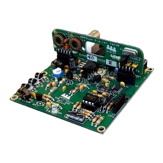
- Page 1 QRPGuys Digital DSB Transceiver Kit, w/smd mixer First, familiarize yourself with the parts and check for all the components. If a part is missing, please contact us at qrpguys.parts@gmail.com and we will send you one. Please read all the instructions before starting to assemble the transceiver.
- Page 2 Q1, Q2, Q4, Q6, Q7, Q8 BS170 TO-92 MOSFET Q3, Q9 2N3904 TO-92 NPN 2N3906 TO-92 PNP R11, R20 5.6 OHMS GRN/BLUE/GOLD/GLD 51 OHMS GRN/BRN/BLK/GLD R10, R19 470 OHMS YEL/VIO/BRN/GLD R4, R9, R18, R21 BRN/BLK/RED/GLD 4.7K YEL/VIO/RED/GLD R2, R3, R12, R16, R17 BRN/BLK/ORG/GLD YEL/VIO/ORG/GLD R6, R8...
- Page 3 INDUCTORS 0.68 uH BLU/GRY/SIL/GLD or BLU/GRY/SIL/SIL 1.2 uH BRN/RED/GLD/GLD or BRN/RED/GLD/SIL 2.2 uH RED/RED/GLD/GLD or RED/RED/GLD/SIL T37-2 RED CORES T37-6 YELLOW CORES crystals 7.074 MHz HC-49/US 10.136 MHz HC-49/US 14.074 MHz HC-49/US Miscellaneous Band module boards #26 magnet wire 1’ #26 magnet wire, diff.
- Page 4 Assembly: The first step is to sort the parts into groups of similar types. This will make finding the needed part type and value quicker. All components mount on the front side of the pcb. The first item to install is the only SMD component. We needed to change from the DIP8 form to the SO8 surface mount form because of shrinking availability and to keep the kit low priced.
- Page 5 Resistors: Caution: Several of the values have very similar color codes and differ only by the zero multiplier color. It is also easy to mix up the 51 and 1 Meg resistors as 51 is green/black/brown/gold and 1 meg is brown/black/green/gold. L4 is a RF choke.
-
Page 6: Everything Else
Everything else: [ ] U3 – 7809 Bend the leads at the point where they narrow. Secure with 4-40 screw and nut. [ ] J5, J6, J7 – 5 pins SIP socket. Make sure these are set square to the board before soldering more than one pin. - Page 7 Special Note: Do not proceed until you make this check. If you have installed T1 correctly, you should read 0 ohms with an ohm meter between the two pads marked by the red arrows on T1. If you have installed T2 correctly, you should read 0 ohms with an ohm meter between the two pads marked by the blue arrows on T2.
- Page 8 Note: When reading module capacitor values, do not confuse the manufacturing codes with the component value. If it looks strange, it may be a manufacturing code, look on the other side of the component. Be sure you have read the values correctly. Sort all the capacitors out before you start assembling them onto the modules.
- Page 9 [ ] L1 – 0.68 uH – Blue/Gray/Silver/Gold or Blue/Gray/Silver/Silver [ ] C26 – 100pfd – marked 101 [ ] C27 – 22 pfd – marked 22 or 220 [ ] C28 – 22 pfd – marked 22 or 220 [ ] C29 –...
- Page 10 You are now ready for on-air testing. [ ] Start the WSJT-X program on your PC or Laptop. [ ] Make the required MIC and Headphone connections between the PC and DSB board. MIC to MIC and PHONES to PHONES. (I found nice stereo jumper cables at the Dollar Store). [ ] Plug in the desired band module.
-
Page 11: Theory Of Operation
Theory of operation: The Digital DSB transceiver is built around the ubiquitous SA602/612A mixer-oscillator chip. It provides both the receive and transmit functions. Receiver: The antenna is first routed through the transmitter's Low Pass Filter (LPF) and then into a BS170 MOSFET, which is the receiver input T/R switch. -
Page 12: Troubleshooting
Trouble shooting: Soldering issues are the most common reason for a board not to work the first time. A careful visual inspection will often locate the problem. Ground pads take a little extra heat compared to other pads, so take note of these. Solder can stick to the component lead, but not flow into the hole. - Page 13 X-ray view of board. “floating” pads are connected to ground plane, not shown for clarity. D=Drain G=Gate S=Source E=Emitter B= Base C=Collector I=Input G=Ground O=Output D / C G / B S / E D / C G / B S /E Q6/7/8 9V ~2.5V 0V 0.78V...
- Page 14 Page 14 of 16 ft8_II_assy_smd_diode_072020.pdf...
- Page 15 Page 15 of 16 ft8_II_assy_smd_diode_072020.pdf...
- Page 16 In the table below are some “modeled” values for additional bands to experiment with. Some tweaking may be required. You will need to source your own components. If you choose to model your own high pass filter (L1 & C26), be sure to add the 88pF stray capacitance inherent in the design to C26.