
Related Manuals for Sony FPF55C17196UA


Summary of Contents for Sony FPF55C17196UA
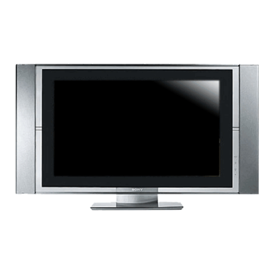
- Page 1 KDE55XBR950 PANEL MODULE SERVICE MANUAL UC Model PDP Module Name FPF55C17196UA FLAT PANEL COLOR TV...
- Page 2 CONTENTS 1 OUTLINE ..........................1 1.1 Panel Dimension ........................ 1 1.2 Feature ..........................1 1.3 Specification ........................2 1.3.1 Functional specification ....................2 1.3.2 Display quality specification ..................3 1.3.3 I/O Interface Specification.................... 4 2 SAFETY HANDLING of THE PLASMA DISPLAY ..............8 2.1 Notes to Follow During Servicing ..................
- Page 3 6.2.5 Logic board parameter forwarding ..................74 6.2.6 Accumulation time reset ......................76 6.2.7 Setup before shipment ......................77 7 The parts information..........................78 7.1 FPF55C17196UA-53 configuration list ..................78 8 packing Procedure ..........................79 8.1 Single packing ..........................79 ...
- Page 4 Scope; 55P1 series (Model name; FPF55C17196UA) Caution Before doing the service operation please be sure to read this service analysis manual. This module has a lot of devices to secure the safety against the fire, electric shock, injury and harmful radiation.
-
Page 5: Panel Dimension
1 OUTLINE The module is a plasma display module which can be designed in there is no fan in addition to a general feature of the plasma display such as a flat type, lightness, and high-viewing-angle and terrestrial magnetism. PANEL DIMENSION 1340(Glass) 1229.4 Sub- pixel pitch(horizontal) -
Page 6: Functional Specification
1.3 SPECIFICATION 1.3.1 Functional specification Specification Item UA-5* Externals Module size 1340 × 760 × 66mm Weight 30kg Display panel Display size 1229.4 × 691.2mm (55inch: 16:9) Resolution 1366 × 768 pixel Pixel pitch 0.90(H) × 0.90(V)mm Sub pixel pitch 0.30(H) ×... - Page 7 1.3.2 Display quality specification Specification Item UC-5* Non-lighting cell Total number (subpixel) 15 or less defect Density (subpixel/cm 2 or less (However,1 continuousness or less) Size (H x V) (subpixel) 1x2 or less, Or 2x1 or less Non-extinguishing Total number (subpixel) 6 or less(each color 2 or less)...
- Page 8 1.3.3 I/O Interface Specification (1) LVDS Signal Definition and Function A video signal (display data signal and control signal) is converted from parallel data to serial data with the LVDS transmitter and further converted into four sets of differential signals before input to this product.
- Page 9 (2) Video Signal Definition and Function The table below summarizes the definitions and functions of input video signals before LVDS conversion. Number Input/ Item Signal name Signal definition and function of signals output Display data signal Original DATA-RA Video signal RA9/GA9/BA9 is the highest intensity bit.
- Page 10 (3) Connector Specification The connector specification is shown below. Please do not connect anything with the terminal NC. (3-1) Signal connector [CN1] Pin No. Signal name Pin No. Signal name RA0- GND(LVDS) RA0+ RA1- RA1+ RA2- GND(LVDS) RA2+ CPUGO RACLK- PDPGO RACLK+ RA3-...
- Page 11 (3-3) Power Source Connectors (PSU only is used on repair working) (a) Power input / Signal control connector [CN3] Pin No. Symbol N.C. VSAGO VCEGO B11B-PH-SM3-TB (Maker: JST) Vpr2 [Conforming connector] Housing: PHR-11 Contact: SPH-002T-P0.5L (b) Power supply output connector for system [CN21] Pin No.
- Page 12 2 SAFETY HANDLING of THE PLASMA DISPLAY 2.1 NOTES TO FOLLOW DURING SERVICING The work procedures shown with the Note indication are important for ensuring the safety of the product and the servicing work. Be sure to follow these instructions. Before starting the work, secure a sufficient working space.
-
Page 13: Name And Function
3 NAME and FUNCTION 3.1 CONFIGURATION ABUS-U1 Signal Cable Signal Cable ABUS-U4 Serial ID Label P.S. Cable ABUS-U2 ABUS-U3 Product Label Signal Cable P.S. Cable LOGIC X-SUS Y-SUS Signal Cable ABUS-D2 ABUS-D1 ABUS-D4 Signal Cable ABUS-D3 P.S. Cable... -
Page 14: Block Diagrams
3.2 Block Diagrams 3.2.1 Signal Diagrams CNU3-7 CNU3-8 X X X X - - - - SUS SUS B. B. B. B. Y Y Y Y - - - - SUS SUS B. B. B. B. X-SUS ABUS U3 ABUS U3 ABUS U1 ABUS U1.... - Page 15 3.2.2 Power Diagrams X X X X - - - - SUS SUS B. B. B. B. Y Y Y Y - - - - SUS SUS B. B. B. B. CNU4-5 Vcc 5V CN23 ABUS U1. . . . ABUS U1 ABUS U1 ABUS U1...
- Page 16 3.3 FUNCTION 3.3.1 Logic board Function (1) Data Processor - γ adjustment(1 / 2.2 / 2.4 / 2.6 / 2.8) - NTSC/EBU format(Color matrix) Switch - RGB gain Control(White balance adjustment, Amplitude limitation) - Error Diffusion Technology(Grayscale adjustment) - Dither(Grayscale adjustment) - Burn-in Pattern generation (2) Data Converter - Quasi out-line adjustment (luminous pattern control)
- Page 17 3.3.2 Function of X-SUS Board (1) DC/DC power supply block Vs (+85V) Vw (+190V) / Vx (+40V) / Vu (+35V) / Vq (-40V) Vcc (+5V) Vex (+16V) / XFve (+18V, floating) (2) X switching block Switching during address period Switching during sustain period Switching during reset period (3) Current detector block Isx (sustain) current detection...
-
Page 18: Protection Function
3.4 PROTECTION FUNCTION Reactivation State of protection operation condition when (√:State change、 、 、 、 There is no change at the blank.) abnormal content is excluded Abnormality part State Re-turn ing on √ √ √ √ √ √ √ Overvoltage Stop(no latch) √... -
Page 19: Problem Analysis
4 PROBLEM ANALYSIS 4.1 OUTLINE OF REPAIR FLOW Client claim Client Repair product Recheck the problem description and Claim contents match Product block/PDP module block Locating cause of problem Product manufacturer (Repair center) Is PDP module block Product problem analysis/Repair Defective ? PC board replacement/Parts replacement... - Page 20 4.2 OUTLINE OF PDP MODULE REPAIR FLOW Receipt of returned product (Chapter 4.3) Does ID of Repair description and returned returned product agree with ID product rechecked. of actual Appearance check Appearance unacceptable (NG) ? Repair of appearance requested ? Perform operation test (Chapter 4.4).
- Page 21 Fault mode classification (Chapter 4.5) Fault analysis (Chapter 4.6) Repair of faulty spots (Chapter 5) Replace LOGIC PC board or panel chassis ? Adjustment (Chapter 6) Perform operation test (Chapter 4.4) Problem repaired? Warranty test (Running) End of repair Shipment -17-...
- Page 22 Problem symptom nonrecurrence analysis mode/Shipment process mode Implement module tapping Problem recurs ? Perform running test (Burn-in pattern) Problem recurs ? Turn off the main power -18-...
- Page 23 4.3 CHECKING THE PRODUCT REQUESTED FOR REPAIR Check the serial ID number of the product requested for repair before starting the problem analysis and repair. Structure of serial ID number is shown below. (1) Checking serial ID number of PDP module (14 digits) The serial ID number of the product that is brought in for service and that of the completed panel chassis has the structure as shown below.
- Page 24 4.4 OPERATION TEST PROCEDURE (1) Prepare the test equipment. (2) Set the PSU board (PS-jig) by five M3X8 screw on the module of requestedfor repair. (photo4.1) (3) Connect the cable connector from PSU board to CN9 on logic board and CN21 on XSUS board. (photo4.2) (4) Set the module of requested repair to a stand.
- Page 25 PDPgo switch Select switch of Display size, Photo 4.3 Synchronous, and Clock signal < State of initialization> -21-...
-
Page 26: Fault Symptom
4.5 FAULT SYMPTOM Fault Fault status Suspected Analysis contents fault location procedure measure Entire screen After momentarily going on, the X-SUS,Y-SUS Refer to does not light. screen becomes black PSU, Panel Chapter immediately or after a few chassis, Logic 4.6.1 ABUSL or R seconds. - Page 27 Fault contents Fault status Suspected Analysis fault location procedure and measure Horizontal line hall horizontal line Panel chassis Replace Panel does’nt light or one horizontal (SDM) chassis line does not light from the effective scan area. Every other line does’nt light X-SUS Replace on entire screen.
- Page 28 Fault contents Fault status Suspected Analysis fault procedure and location measure Picture Logic Replace logic board distorted Steps Luminance linearity is Logic Replace logic board gradarion poor skipped Abnormal Abnormal sound X-SUS locations are Y-SUS exchanged Panel External Logic Replace logic Adjustment γ...
- Page 29 4.6 PROBLEM ANALYSIS PROCEDURE 4.6.1. "The entire screen does not light (Main power is turned off)” Problem analysis procedure The entire screen does not light. (Main power is turned off.) PC for analysis Analysis using PC Connected? Chapter 4.7 Remove CN9 (LOGIC) Turn on AC power.
- Page 30 X-SUS board X-SUS board is CN21 (3)-(5) pins or defective. CN21 (7)-(8) pins are shorted. CN21 Switching circuit (power supply) (3)(4) : Vcc has short-circuit. (5)(6)(7)’: GND (8)(9)(10) : Vs Y-SUS board CN31 (4)-(6) pins or CN31 (7)-(8) pins are shorted. CN31 Remove SDM from the (2)(3)(4): Vs...
- Page 31 1pin ABUSD4 board CND4-5 (1)-(7) or CND4-5 CND4-5 (5)-(7) short. CND4-5 (1)(2): Va Disconnect the following (3) (4)(5): Vcc connectors.* CND2-4(ABUS-D2) (6)(7): GND CND3-5(ABUS-D3) CND3-10(ABUS-D3) Each ABUS-D* board CND2-4 (1)-(7) or (5)-(7) ADM is defective CND2-9 (1)-(7) or (5)-(7) (Panel chassis is CND3-12 (1)-(7) or (5)-(7) defective.) CND4-3 (1)-(7) or (5)-(7)
- Page 32 Turn on AC power. PSU board ADM is defective. Va (63V) exist? ADM chip has abnormality. Turn off the AC power. Disconnect CNU4-5(ABUSU4). Turn on AC power. ABUSU1-4 boards PSU board are defective. Va (63V) exist? Power supply line has abnormality. (Ex.
- Page 33 Disconnect between SDM and Y-SUS Measure of SDM power line resistor (A1-A2, B1-B2, C1-C2, D1-D2) SDM is defective. Does SDM power (Panel chassis is supply line short? defective.) SDM chip operation is abnormal. Turn on AC power. PSU board Turn off the Vs (85V) and Vcc AC power.
- Page 34 Disconnect between XBB and X-SUS Measure of XBB line resistor (A1-B1, B1-A2, A2-B2, B2-A3, A3-B3, B3-A4, A4-B4) XBB is defective. (Panel Does XBB line chassis is defective.) short? X-SUS board is defective. Y-SUS board is defective. X-SUS board is defective. Turn off the AC power.
- Page 35 4.6.2 "Vertical line/Vertical bar" Problem analysis procedure Vertical line/Vertical bar LOGIC ~ ABUS board signal Signal cable is cable has abnormal appearance? defective. ADM flexible has abnormal ADM is defective. appearance? (Panel chassis is defective.) Turn on the power. End of analysis Tap lightly on ADM flexible One vertical line?...
- Page 36 Bar of 1/2 width on the upside does not light? Voltage exists at LOGIC board is ABUSU4 board defective. CN U4-5. Turn off the power. Disconnect CNU4-5 on the ABUSU4 board. Turn on the power. Voltage exists ABUSU* board is at PSU Side? defective.
- Page 37 Vertical line of different color does appear? Exists on half upside? Turn off the power. Replace ABUSU board (Backup part). Turn on the main power. Normal? ABUSU board is defective. Turn off the power. Replace LOGIC board (Backup part) Turn on the power. Normal? LOGIC board is defective.
- Page 38 Turn off the power. Replace ABUSD board (Backup part). Turn on the power. ABUSD board is Normal? defective. Turn off the power. Replace LOGIC board (Backup part). Turn on the power. Normal? LOGIC board is defective. Turn off the power. Replace signal cables between LOGIC and ABUS.
- Page 39 4.6.3 "Horizontal bar" Problem analysis procedure Horizontal bar Turn off the power. Replace Y-SUS board (Backup part). Turn on the power. Y-SUS board is Normal? defective. Turn off the power. Replace Y-SUS board (Defective product). Replace X-SUS board (Backup part) Turn on the power.
- Page 40 4.7 PROBLEM ANALYSIS USING A PERSONAL COMPUTER 4.7.1 Connecting a computer (1) Set the module in accordance with Chapter 4.4. (2) Connect the RS-232C terminal of the computer to the RS-232C terminal of the interface board. (3) Turn on the main power to the interface board. (Red LED goes on.) POWER indicator (red LED) 4.7.2 Preparing a computer (1) Turn on the main power to the computer.
- Page 41 4.7.3 Problem Analysis Procedure (1) Select the problem analysis menu from the main menu using the ↑key or ↓key and press <ENTER> key to start the program. Main menu (2) Check the error code (hexadecimal number) from the Latest error code read-out menu and locate the faulty position from the following table.
- Page 42 Error code table Detect Suspected faulty board position (In the order of higher probability of defect) Contents Remarks code (board) LOGIC STANDBY power is stopped PSU temperature has probably increased LOGIC ROM data of waveform is abnormal LOGIC 3.3V power voltage has dropped LOGIC 3.3V power startup is faulty X-SUS...
- Page 43 Suspected faulty board Detect Contents (In the order of higher probability of defect) position Remarks code Contents (board) Va power current is excessive (during ADM1-8 ABUS PSU LOGIC Excess current is operation) detected in ACCC operation. ADM-D1 ADM-D1 has abnormal heat generation. ADM-D1 PSU LOGIC It can possibly occur depending...
-
Page 44: Disassembling And Reassembling
5 DISASSEMBLING AND REASSEMBLING Unless otherwise specified, use the torque screwdriver for screw tightening, following the tightening torques. Screw size Tightening torque 0.69±0.049Nm (7±0.5kg·cm) 1.18±0.098Nm (12±1.0kg·cm) 5.1 Exploded View ⑱ ② ⑭ ⑲ ⑧ ⑲ ⑬ ⑲ ⑦ ⑰ ⑯ ③... - Page 45 5.2 X-SUS Circuit Board Removal/Installation Procedure When removing the circuit board after the main power is turned on/off, wait for at Note least four minutes before starting to remove the circuit board. If the circuit board removal is started immediately after turning off the main power, it can result in electric shock or damage to the circuit due to residual electric charge.
- Page 46 ③ Note Pick up Pick up Pick up and release upper the lock of space holder (rod). Moreover, confirm the lock surely combines intuition when you install the board. Space holder (rod) -42-...
- Page 47 5.3 Y-SUS Circuit Board Removal/Installation Procedure When removing the circuit board after the main power is turned on/off, wait for at least four minutes before starting to remove the circuit board. Note If the circuit board removal is started immediately after turning off the main power, it can result in electric shock or damage to the circuit due to residual electric charge.
- Page 48 ④ Note Pick up Pick up Pick up and release upper the lock of space holder (rod). Moreover, confirm the lock surely combines intuition when you install the board. Space holder (rod) -44-...
- Page 49 5.4 ABUS-U1 Circuit Board Removal/Installation Procedure When removing the circuit board after the main power is turned on/off, wait for at least four minutes before starting to remove the circuit board. Note If the circuit board removal is started immediately after turning off the main power, it can result in electric shock or damage to the circuit due to residual electric charge.
- Page 50 ⑤ Note Pick up and release upper the lock of space holder (rod). Moreover, confirm the lock surely Pick up Pick up combines intuition when you install the board. Space holder (rod) -46-...
- Page 51 5.5 ABUS-U2 Circuit Board Removal/Installation Procedure When removing the circuit board after the main power is turned on/off, wait for at least four minutes before starting to remove the circuit board. Note If the circuit board removal is started immediately after turning off the main power, it can result in electric shock or damage to the circuit due to residual electric charge.
- Page 52 ⑥ Note Pick up Pick up Pick up and release upper the lock of space holder (rod). Moreover, confirm the lock surely combines intuition when you install the board. Space holder (rod) -48-...
- Page 53 5.6 ABUS-U3 Circuit Board Removal/Installation Procedure When removing the circuit board after the main power is turned on/off, wait for at least four minutes before starting to remove the circuit board. Note If the circuit board removal is started immediately after turning off the main power, it can result in electric shock or damage to the circuit due to residual electric charge.
- Page 54 ⑦ Note Pick up Pick up Pick up and release upper the lock of space holder (rod). Moreover, confirm the lock surely combines intuition when you install the board. Space holder (rod) -50-...
- Page 55 5.7 ABUS-U4 Circuit Board Removal/Installation Procedure When removing the circuit board after the main power is turned on/off, wait for at least four minutes before starting to remove the circuit board. Note If the circuit board removal is started immediately after turning off the main power, it can result in electric shock or damage to the circuit due to residual electric charge.
- Page 56 ⑧ Note Pick up and release upper the lock of space Pick up Pick up holder (rod). Moreover, confirm the lock surely combines intuition when you install the board. Space holder (rod) -52-...
- Page 57 5.8 ABUS-D1 Circuit Board Removal/Installation Procedure When removing the circuit board after the main power is turned on/off, wait for at least four minutes before starting to remove the circuit board. Note If the circuit board removal is started immediately after turning off the main power, it can result in electric shock or damage to the circuit due to residual electric charge.
- Page 58 ⑨ Note Pick up Pick up Pick up and release upper the lock of space holder (rod). Moreover, confirm the lock surely combines intuition when you install the board. Space holder (rod) -54-...
- Page 59 5.9 ABUS-D2 Circuit Board Removal/Installation Procedure When removing the circuit board after the main power is turned on/off, wait for at least four minutes before starting to remove the circuit board. Note If the circuit board removal is started immediately after turning off the main power, it can result in electric shock or damage to the circuit due to residual electric charge.
- Page 60 ⑩ Note Pick up Pick up Pick up and release upper the lock of space holder (rod). Moreover, confirm the lock surely combines intuition when you install the board. Space holder (rod) -56-...
- Page 61 5.10 ABUS-D3 Circuit Board Removal/Installation Procedure When removing the circuit board after the main power is turned on/off, wait for at least four minutes before starting to remove the circuit board. Note If the circuit board removal is started immediately after turning off the main power, it can result in electric shock or damage to the circuit due to residual electric charge.
- Page 62 ⑪ Note Pick up and release upper the lock of space Pick up Pick up holder (rod). Moreover, confirm the lock surely combines intuition when you install the board. Space holder (rod) -58-...
- Page 63 5.11 ABUS-D4 Circuit Board Removal/Installation Procedure When removing the circuit board after the main power is turned on/off, wait for at least four minutes before starting to remove the circuit board. Note If the circuit board removal is started immediately after turning off the main power, it can result in electric shock or damage to the circuit due to residual electric charge.
- Page 64 ⑫ Note Pick up Pick up Pick up and release upper the lock of space holder (rod). Moreover, confirm the lock surely combines intuition when you install the board. Space holder (rod) -60-...
- Page 65 5.12 LOGIC Circuit Board Removal/Installation Procedure Remove the circuit board following the steps below. To install the circuit board, reverse the removal procedure. (1) Release the lock of CN4, CN5, CN6, CN7, and then reconnect the signal cable (FPC). by lifting the lock (2) Release the lock of CN3 and then reconnect signal cable.
- Page 66 ② Note Pick up Pick up Pick up and release upper the lock of space holder (rod). Moreover, confirm the lock surely combines intuition when you install the board. Space holder (rod) -62-...
- Page 67 5.13 Complete Panel chassis Removal / Installation Procedure (1) Remove the board of 11 types (X-SUS, Y-SUS, ABUS-U1, U2, U3, U4, D1, D2, D3, D4, and LOGIC) that are installed in the panel module. For the removal procedure, refer to section 5.2 to 5.7. Note: Before removing the board of 11 types, be sure to release the three power supply cables and tweleve FFC cables (White color).
- Page 68 (2) Install the 11 tpyes boards that were removed by step (1) at panel chassis of repair part. (Refer to t he disassembly figure shown in Section 5.1) (3) Print the serial ID number of the product to be repaired on the product label which is prepared separately.
- Page 69 (4) After the installation of the board is complete, connect the cables as shown below photo. Fix the power supply cable at the cable clamp. Expansion photo. -65-...
- Page 70 6 OPERATION CHECK AND ADJUSTMENT METHOD 6.1 LIST OF CHECK AND ADJUSTMENT ITEMS (Reference) When X-SUS When Y-SUS When LOGIC When ABUS When PSU Adjustment item Adjustment item When PDP (Name of the part) board is board is board is board is board is Jig/tools...
-
Page 71: Check And Adjustment Procedure
6.2 CHECK AND ADJUSTMENT METHOD 6.2.1 Check and adjustment procedure Check and adjustment Was LOGIC board replaced? Logic board data transfer (Section 6.2.5) Was Panel chassis replaced? Parameter adjustment (Section 6.2.2) Operation and Performance check Normally? Burn-inmode setting (Section 6.2.4) Heat run (Setion 6.2.4) Abnormal operation? -
Page 72: Parameter Adjustment
6.2.2 Parameter adjustment List of parameter adjustment items Measurement item Adjusment items parameter Adjustment value (conditions) Remarks point Vs Voltage X-SUS Voltage setting label indication value* ; ±1% (all black) Va Voltage X-SUS Voltage setting label indication value* ; ±2% (all black) Vw Voltage X-SUS Voltage setting label indication value* ;... - Page 73 (1) From the main menu, select the voltage adjustment menu with the ↑ key or ↓ key and press the <ENTER> key. Main menu Module information menu POWER ON menu Problem analysis menu →Voltage adjustment menu Accumulated power-on time menu Logic board change menu EXIT (2) From the voltage adjustment menu, adjust parameters in the order starting from Vs, Va, Vw, Vx, Vq,...
- Page 74 6.2.3 Operation performance check items (1) Environmental conditions Temperature: Room temperature Judgment distance: 1 meter from panel screen Preheat run: 5 minutes with entire screen lit (white) (2) Test patterns: PSEL Push SW Display pattern Size Details White screen 24 × 24 Cross slash Large Vertical stripe...
-
Page 75: Power On/Off
(3) Judgment Item Test items Test signal Judgment criterion Brightness non-uniformity White screen (W) Brightness non-uniformity in the form of stripes must not be visible in vertical and horizontal directions. Black noise Horizontal gray scale Rank 3 or higher in the 5-step evaluation. (Each color of R/G/B) <Rank>... -
Page 76: Heatrun Test
6.2.4 Heat Run Test (1) Set the module by following the same procedure as that for Problem Analysis in Section 4.7. (2) From the main menu, select the POWER ON menu with the ↑ key or ↓ key and press the <ENTER>... - Page 77 (4) To change the internal pattern, select the internal pattern selection from the POWER ON menu using the ↑(up) or ↓(down) key, and press the <ENTER> key. Setup Display pattern Setup Display pattern value value 01 to 08 patterns are displayed every 2 Entire screen is cyan seconds.
- Page 78 6.2.5 Logic board parameter forwarding (1) The module is set according to the same to failure analysis procedure in clause 4.7. The logic board before being exchanged is installed in the module. (2) From the main menu, select change Logic board menu with the ↑ key or ↓ key and press the <ENTER>...
- Page 79 (5) From the logic board change menu, select data paste with the ↑ key or ↓ key and press the <ENTER> key. Data is written in the exchanged Logic board. Logic board change menu (6) Select RETURN with ↑ key or ↓ key and press <ENTER> key to return to the menu screen.
- Page 80 6.2.6 Accumulation time reset (1) The module is set according to the same to failure analysis procedure in clause 4.7. (2) From the main menu, select Power-on time menu with the ↑ key or ↓ key and press the <ENTER> key. Main menu (3) From the Power-on time menu, select Operation hours with the ↑...
- Page 81 6.2.7 Setup before shipment Before shipment from service, perform the following setup or initialization. 1) Initial values that are shown in the List of EEPROM contents in Section 3.3.1. (Main power of the module is turned off.) Clearing the error codes Select EXIT menu with the ↑...
-
Page 82: The Parts Information
7 THE PARTS INFORMATION 7.1 FPF55C17196UA-53 CONFIGURATION LIST Model Repair Parts List Model name Panel Module type Part Number Description Note (Supplier's parts name) KDE55XBR950 (U/C) FPF55C17196UA -53 A-1078-433-A PDP Module Assy 1-789-051-11 X-SUS board FPF24R -XSS0018 1-789-052-11 Y-SUS board... -
Page 83: Packing Procedure
8 PACKING PROCEDURE 8.1 Single Packing -79-... - Page 84 2004FL08-Data Sony EMCS Corporation Made in Japan Ichinomiya TEC 2004. 6 9-878-253-01...