Table of Contents
Advertisement
SERVICE MANUAL
Ver. 1.1 2011.04
• HBD-E280 is the amplifi er, video, HDMI, BD/DVD/Super Audio CD/CD system, USB, LAN and FM tuner section in BDV-E280.
• HBD-T28 is the amplifi er, video, HDMI, BD/DVD/Super Audio CD/CD system, USB, LAN and FM tuner section in BDV-T28.
Amplifier Section
U.S.models:
AUDIO POWER SPECIFICATIONS
POWER OUTPUT AND TOTAL HARMONIC
DISTORTION:
(FTC)
Front L + Front R:
With 3 ohms loads, both
channels driven, from 180
- 20,000 Hz; rated 60 watts
per channel minimum
RMS power, with no more
than 1% total harmonic
distortion from 250 milli
watts to rated output.
Other models:
POWER OUTPUT (rated)
Front L/Front R:
108 W + 108 W (at 3 ohms,
1 kHz, 1% THD)
POWER OUTPUT (reference)
Front L/Front R/Center/Surround L/Surround R:
167 W (per channel at
3 ohms, 1 kHz)
Subwoofer:
165 W (at 3 ohms, 80 Hz)
Inputs (Analog)
AUDIO (AUDIO IN)
Sensitivity: 450/250 mV
Inputs (Digital)
TV (Audio Return Channel/OPTICAL)
Supported formats: LPCM
2CH (up to 48 kHz), Dolby
Digital, DTS
HDMI (IN 1)/HDMI (IN 2)
Supported formats: LPCM
2CH (up to 96 kHz), Dolby
Digital, DTS
9-893-108-02
Sony Corporation
2011D05-1
©
2011.04
Published by Sony Techno Create Corporation
HBD-E280/T28
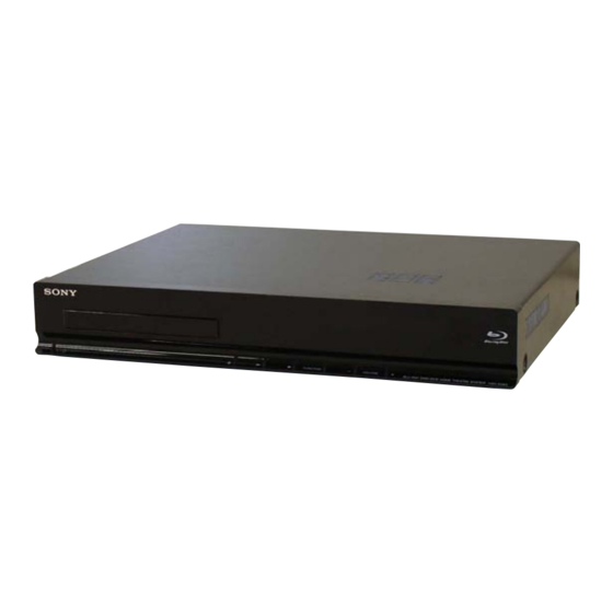
Photo: HBD-E280
Model Name Using Similar Mechanism
Mechanism Type
Optical Pick-up Block Name
SPECIFICATIONS
Video Section
Outputs
VIDEO: 1 Vp-p 75 ohms
HDMI Section
Connector
Type A (19pin)
BD/DVD/Super Audio CD/CD System
Signal format system
U.S. and Canada models: NTSC
Other models:
NTSC/PAL
USB Section
(USB) port:
Type A (For connecting
USB memory, memory
card reader, digital still
camera, and digital video
camera)
LAN Section
LAN (100) terminal
100BASE-TX Terminal
FM Tuner Section
System
PLL quartz-locked digital
synthesizer
Tuning range
U.S. and Canada models: 87.5 MHz - 108.0 MHz
(100 kHz step)
Other models:
87.5 MHz - 108.0 MHz (50
kHz step)
Antenna (aerial)
FM wire antenna (aerial)
Antenna (aerial) terminals 75 ohms, unbalanced
BLU-RAY DISC/DVD RECEIVER
US Model
AEP Model
UK Model
Australian Model
PX Model
HBD-E280
Canadian Model
Mexican Model
HBD-E280/T28
BDP-S380
BPX-6
KEM-470AAA
General
Power requirements
U.S. and Canada models: 120 V AC, 60 Hz
European and Australian models:
220 V - 240 V AC,
50/60 Hz
Other models:
110 V - 240 V AC,
50/60 Hz
Power consumption
On: 160 W
Standby: 0.3 W (at the
Power Saving mode)
Dimensions (approx.)
400 mm × 65 mm × 315
mm (15
3
/
in × 2
4
1
12
/
in) (w/h/d) incl.
2
projecting parts
Mass (approx.)
3.3 kg (7 lb 5 oz)
Design and specifications are subject to change
without notice.
Standby power consumption 0.3W.
Over 85% power efficiency of amplifier block is
achieved with the full digital amplifier, S-Master.
5
/
in ×
8
Advertisement
Table of Contents

Related Manuals for Sony HBD-E280


Summary of Contents for Sony HBD-E280
- Page 1 Photo: HBD-E280 • HBD-E280 is the amplifi er, video, HDMI, BD/DVD/Super Audio CD/CD system, USB, LAN and FM tuner section in BDV-E280. • HBD-T28 is the amplifi er, video, HDMI, BD/DVD/Super Audio CD/CD system, USB, LAN and FM tuner section in BDV-T28.
- Page 2 “AVCHD” and the “AVCHD” logo are trademarks of Panasonic Corporation and Sony Corpora- tion. protective housing inside the • , “XMB,” and “xross media bar” are trademarks of Sony Corporation and Sony Computer enclosure. Entertainment Inc. • “PLAYSTATION” is a trademark of Sony Computer Entertainment Inc.
-
Page 3: Table Of Contents
HBD-E280/T28 TABLE OF CONTENTS SERVICING NOTES 5-10. Schematic Diagram - MB-141 Board (2/12) - ....37 ..........5-11. Schematic Diagram - MB-141 Board (3/12) - ....38 5-12. Schematic Diagram - MB-141 Board (4/12) - ....39 DISASSEMBLY 5-13. Schematic Diagram - MB-141 Board (5/12) - ....40 2-1. -
Page 4: Servicing Notes
HBD-E280/T28 SECTION 1 SERVICING NOTES NOTE OF REPLACING THE IC101, IC304, IC307, NOTES ON HANDLING THE OPTICAL PICK-UP IC501, IC702, IC5301 AND IC5307 ON THE MB-141 BLOCK OR BASE UNIT BOARD IC101, IC304, IC307, IC501, IC702, IC5301 and IC5307 on the The laser diode in the optical pick-up block may suffer electro- MB-141 board cannot exchange with single. - Page 5 HBD-E280/T28 NOTE OF REPLACING THE OPTICAL DEVICE (KEM- 1-3. Barcode decoder (BDPRdec) 470AAA) OR MB-141 BOARD Part No. : J-6090-212-A Jig name : BDPRdec.exe The password will be supplied to only service HQ, and Release : 2010.11.26 service center name, q’ty and all of software registered Version : 2.0.0.0...
- Page 6 HBD-E280/T28 2. Pass-fail judgment of the optical device (KEM-470AAA) Perform pass-fail judgment to judge whether the repair of the optical device (KEM-470AAA) is necessary. 2-1. Flow of drive section check Confirm whether the Confirm F5301 to Confirm whether drive voltage is the...
- Page 7 HBD-E280/T28 3. Optical device (KEM-460AAA) replacement Flow of replacement: Note: The photo in fl ow is an image. Save the text data to USB memory Barcode label on (memory capacity new optical device need not be 8GB) (KEM-470AAA) bottom side...
- Page 8 HBD-E280/T28 Ver. 1.1 NOTE THE BD DRIVE (BPX-6) PARTS REPLACING MODEL IDENTIFICATION The mechanism blocks except optical device of BD drive (BPX-6) - Rear view - are chiefl y composed of the following parts. Part No. • CHUCK HOLDER ASSY •...
- Page 9 HBD-E280/T28 NOTE OF REPLACING THE IC3100, IC3200 AND CHECKING METHOD OF NETWORK OPERATION IC3300 ON THE AMP BOARD AND THE COMPLETE It is necessary to check the network operation, when replacing the AMP BOARD MB-141 board. Check the operation of wired LAN, according to When IC3100, IC3200 and IC3300 on the AMP board and the the following method.
- Page 10 HBD-E280/T28 HOW TO OPEN THE TRAY WHEN POWER SWITCH TURN OFF Note 1: After the case (E0) is removed, this work is done. Note 2: Please prepare the thin wire (clip etc. processed as shown in fi gure below). 1 Remove the case (E0).
-
Page 11: Disassembly
HBD-E280/T28 SECTION 2 DISASSEMBLY • This set can be disassembled in the order shown below. 2-1. DISASSEMBLY FLOW 2-2. HOW TO BEND FFC (Page 11) 2-2. CASE (E0) (Page 12) 2-3. LOADING PANEL 2-6. AMP BOARD 2-7. SWITCHING REGULATOR (Page 12) -
Page 12: Case (E0)
HBD-E280/T28 Note: Follow the disassembly procedure in the numerical order given. 2-3. CASE (E0) 6 case (E0) 1 tapping screw 2 five screws (BV3) 5 three claws 1 tapping screw 2-4. LOADING PANEL two holes – Side view – 3 four claws clip etc. -
Page 13: Front Panel Assy
HBD-E280/T28 2-5. FRONT PANEL ASSY 2 five claws 3 front panel assy 1 three screws (BV3) 2-6. BD DRIVE (BPX-6) 4 tapping screw 8 sound sheet 2 wire (flat type) (9 core) (CN2460) 5 three screws 3 wire (flat type) (5 core) (CN2470) -
Page 14: Board
HBD-E280/T28 Ver. 1.1 2-7. MB-141 BOARD front side MB-141 board wire holder 1 wire (flat type) (15 core) (CN6201) 2 two screws (BV3) MB-141 board fan cable qs three screws rear side 3 wire holder (BV3) qs four screws (BV3) -
Page 15: Amp Board
HBD-E280/T28 Ver. 1.1 2-8. AMP BOARD MB-141 board fan cable • Abbreviation : Australian model rear side : Italian model : Mexican model qf four screws (BV3) qg heat sink (S-master DDV) qs connector qh three screws (CN451) (BV3) 4 insulated plate... -
Page 16: Switching Regulator (Swr1)
HBD-E280/T28 Ver. 1.1 2-9. SWITCHING REGULATOR (SWR1) front side switching regulator cable tie (SWR1) HOLD WIRE board 3 two screws 4 HOLD WIRE board (BV3) 1 Cut the cable tie. Note: In reassembling, use new cable tie AMP board to fasten the clamp same as before. -
Page 17: Optical Pick-Up Block (Kem-470Aaa), Wire (Flat Type)
HBD-E280/T28 2-10. OPTICAL PICK-UP BLOCK (KEM-470AAA), WIRE (FLAT TYPE) 4 chuck holder assy (D) 1 two screws 3 two claws (BVTP 2.6) 2 two claws qa insulator 7 two float screws (S) qs optical pick-up block qh ffc holder (rear) -
Page 18: Test Mode
HBD-E280/T28 SECTION 3 TEST MODE COLD RESET FACTORY INITIALIZE The cold reset clears data except BD/DVD data stored in the RAM Return all of the unit setting to their factory defaults. Note 1: Disconnect the following connections when you use this mode. - Page 19 HBD-E280/T28 BD SERVICE MODE 6. The message “Close” appears, and press the [ ] button on the remote commander. [Wireless checking fail on M07.R.179] Due to software bug in M07.R.179, currently Service mode do not sup- port wireless checking features this version of software. For service to Initialize Personal Information confi...
- Page 20 HBD-E280/T28 2. Menu Tree Service Mode Menu Device Test Diag [1] Diag Diag Test US D C IFcon test [2] Log [3] Factory Initialize [4] Network Video Test [5] Version Up Video output test [6] System Information [7] EMC Test Mode...
- Page 21 HBD-E280/T28 3. Service Mode Menu (Top Menu) This is the top menu of service mode. Diag Each function is accessed from this screen. Category: Device Test Operation: Moves to Diag screen Moves to Log screen Diag Moves to Factory Initialize screen...
- Page 22 HBD-E280/T28 6. Diag (Audio Input Test) 8. Diag (MIC Input Test) This screen performs audio input test. This screen performs MIC input test. Note: Not used for the servicing. Screen 1: Select Audio Input Test Category 9. Diag (HDMI Input Test) Operation: This screen performs HDMI input test.
- Page 23 HBD-E280/T28 11. Log: Error Log (Output of each Log) 13. Network (Network Test Diagnosis Screen: Ifconfi g) This screen displays the contents of each log. Network menu for the wired ethernet. Note: Do not refer to the displayed date. Screen 1: Ifconfi g Test...
- Page 24 HBD-E280/T28 Screen 2: The IP address of the Ping point is set up Contents List: (IP address input mode) Model When “Ping to :>” is reversed, the [ ] button is pressed and IP Destination is inputted. Sequence Number Operation:...
- Page 25 HBD-E280/T28 16. Drive CONFIRMATION ITEM This menu is used to operate the drive using drive-related diagnos- 1. Playback Operation Confi rmation tic and tools. 1-1. Test Disc Part No. Description Layer Screen 1: Selecting items under *Drive J-6090-199-A BLX-104 Single Layer...
-
Page 26: Electrical Check
HBD-E280/T28 SECTION 4 ELECTRICAL CHECK 1-2. Playback operation confi rmation FM AUTO STOP CHECK Confi rm operation in each signal/output mode of test disc (BLX- generator 104/204) according to the content of the repair. Note: “AV Sync.” doesn’t operate. 2. Networking Confi rmation Confi... -
Page 27: Diagrams
HBD-E280/T28 Ver. 1.1 SECTION 5 DIAGRAMS 5-1. BLOCK DIAGRAM - SERVO Section - J6001 BD DRIVE VIDEO AMP VIDEO OUT VDACX_OUT C19 (BPX-6) IC6001 BD_RF+ RFIP VSTB L25 BD_RF- RFIN BD DECODER IC101 (1/4) DVD_RF+ RFIP2 DVD_RF- RFIN2 (E280: AEP, IT, UK, AUS, MX/T28: MX) -
Page 28: Block Diagram - Memory Section
HBD-E280/T28 5-2. BLOCK DIAGRAM - MEMORY Section - BD DECODER IC101 (2/4) NS_XTALO X401 27MHz NS_XTALI EEPROM SD-RAM SD-RAM IC6601 IC106 IC206 I2C_SDA VDIN31 DQL0 - DQL7, DQL0 - DQL7, RDQ0 - RDQ15 RDQ0_B - RDQ15_B I2C_SCL VDIN30 DQU0 - DQU7... -
Page 29: Block Diagram - Hdmi Section
HBD-E280/T28 5-3. BLOCK DIAGRAM - HDMI Section - BUFFER Q702 (Page 30) WAVE SHAPER ARC_SPDIF IC5702 CN701 HDMI ARC OUT BD DECODER HDMI INPUT SELECTOR IC101 (3/4) IC5701 RESERVED DATA0+ D0+_1 D0+_SINK CH0_P B16 TMDS DATA0 + D0–_1 D0–_SINK RX0B DATA0–... -
Page 30: Block Diagram - Main Section
HBD-E280/T28 5-4. BLOCK DIAGRAM - MAIN Section - BD DECODER IC101 (4/4) R-ch is omitted due to same as L-ch. ARC_SPDIF F11 SPMCLK/DIN1 (Page 29) SIGNAL PATH : AUDIO : TUNER OPTICAL DIGITAL IN RECEIVER G11 SPBCK/DIN2 OPTICAL IC5901 A/D CONVERTER... -
Page 31: Block Diagram - Amp Section
HBD-E280/T28 5-5. BLOCK DIAGRAM - AMP Section - STREAM PROCESSOR POWER AMP IC3010 IC3100 TB451 AMP_D1 OUTL2 (-) L.P.F. DATA 8 PWM_B OUT_B FRONT L AMP_MCKO 36 XFSIIN OUTL1 (+) L.P.F. PWM_A OUT_A AMP_BCKO 30 BCK OUTR1 (+) AMP_LRCKO 29 LRCK... -
Page 32: Block Diagram - Power Supply Section
HBD-E280/T28 Ver. 1.1 5-6. BLOCK DIAGRAM - POWER SUPPLY Section - Abbreviation (E280: AEP, IT, UK, AUS, MX/T28: MX) AUS : Australian model DC/DC : Italian model FRONT USB +5V CONVERTER IC601 MX : Mexican model DC/DC REAR USB +5V... - Page 33 HBD-E280/T28 Ver. 1.1 THIS NOTE IS COMMON FOR PRINTED WIRING BOARDS AND SCHEMATIC DIAGRAMS. • Circuit Boards Location (In addition to this, the necessary note is printed in each block.) For Printed Wiring Boards. For Schematic Diagrams. Note: Note: • X : Parts extracted from the component side.
-
Page 34: Printed Wiring Board - Mb-141 Board (Side A)
HBD-E280/T28 Ver. 1.1 5-7. PRINTED WIRING BOARD - MB-141 Board (Side A) - • See page 33 for Circuit Boards Location. • : Uses unleaded solder. (E280: AEP, IT, UK, AUS, MX/T28: MX) (Page 54) (Page 54) FRONT DISPLAY BOARD... -
Page 35: Printed Wiring Board - Mb-141 Board (Side B)
HBD-E280/T28 Ver. 1.1 5-8. PRINTED WIRING BOARD - MB-141 Board (Side B) - • See page 33 for Circuit Boards Location. • : Uses unleaded solder. MB-141 BOARD (SIDE B) JL6217 JL6214 JL6211 JL6204 JL1132 JL6213 JL6210 JL1133 JL1130 JL6215... -
Page 36: Schematic Diagram - Mb-141 Board (1/12)
HBD-E280/T28 5-9. SCHEMATIC DIAGRAM - MB-141 Board (1/12) - • See page 65 for IC Pin Function Description. MB-141 BOARD (1/12) IC101 (1/14) IC101 CXD9998G-BB BD DECODER (Chip Size Package) C103 D0DQ0 AE10 DVCC15_IO_1 AG17 JL101 RDQ0 JL2165 DVCC15_IO_1 D0DQ1... -
Page 37: Schematic Diagram - Mb-141 Board (3/12)
HBD-E280/T28 5-10. SCHEMATIC DIAGRAM - MB-141 Board (2/12) - • See page 65 for IC Pin Function Description. MB-141 BOARD (2/12) IC101 (2/14) IC101 CXD9998G-BB BD DECODER (Chip Size Package) D1DQ0 JL2201 DGND RDQ0_B JL221 D1DQ1 JL2202 DGND RDQ1_B D1DQ2... -
Page 38: Schematic Diagram - Mb-141 Board (4/12)
HBD-E280/T28 5-11. SCHEMATIC DIAGRAM - MB-141 Board (3/12) - • See page 55 for IC Block Diagrams. • See page 65 for IC Pin Function Description. MB-141 BOARD (3/12) A12V MB-141 D3.3V BOARD (8/12) SP_OUT (Page 43) 3.3VA MB-141 JL313 BOARD CORE_1.1V... -
Page 39: Schematic Diagram - Mb-141 Board (5/12)
HBD-E280/T28 5-12. SCHEMATIC DIAGRAM - MB-141 Board (4/12) - • See page 65 for IC Pin Function Description. MB-141 BOARD (4/12) CORE_1.1V MB-141 3.3VA IC101 (4/14) BOARD 1.2VA (3/12) IC101 (5/14) BD DECODER (Page 38) BD DECODER R404 (Chip Size Package) 1.2k... -
Page 40: Schematic Diagram - Mb-141 Board (6/12)
HBD-E280/T28 Ver. 1.1 5-13. SCHEMATIC DIAGRAM - MB-141 Board (5/12) - • Waveforms • See page 55 for IC Block Diagrams. • See page 65 for IC Pin Function Description. – MB-141 Board – – AMP Board – IC5907 6 (SCKI) -
Page 41: Schematic Diagram - Mb-141 Board (7/12)
HBD-E280/T28 5-14. SCHEMATIC DIAGRAM - MB-141 Board (6/12) - • See page 55 for IC Block Diagrams. • See page 65 for IC Pin Function Description. MB-141 BOARD (6/12) IC B/D R5761 IC5706 PW5V_SEL EPR2_SEL +5V POWER SELECT EPR1_SEL MB-141... -
Page 42: Schematic Diagram - Mb-141 Board (8/12)
HBD-E280/T28 5-15. SCHEMATIC DIAGRAM - MB-141 Board (7/12) - • See page 55 for IC Block Diagrams. • See page 65 for IC Pin Function Description. MB-141 BOARD (7/12) CN5801 JL831 JL830 R_USB_DP JL829 R_USB_DM MB-141 JL828 BOARD R_USB_VBUS JL801... -
Page 43: Schematic Diagram - Mb-141 Board (9/12)
HBD-E280/T28 5-16. SCHEMATIC DIAGRAM - MB-141 Board (8/12) - • See page 40 for Waveforms. • See page 55 for IC Block Diagrams. • See page 65 for IC Pin Function Description. MB-141 BOARD (8/12) CL5901 CL5903 IC B/D IC B/D... -
Page 44: Schematic Diagram - Mb-141 Board (10/12)
HBD-E280/T28 5-17. SCHEMATIC DIAGRAM - MB-141 Board (9/12) - • See page 65 for IC Pin Function Description. MB-141 BOARD (9/12) R1195 RB1102 R1172 CN5102 IC101 (12/14) RB1101 R1173 JL1129 3.3V BD DECODER JL1130 JL1131 (Chip Size Package) IC101 (NC) -
Page 45: Schematic Diagram - Mb-141 Board (11/12)
HBD-E280/T28 5-18. SCHEMATIC DIAGRAM - MB-141 Board (10/12) - • See page 40 for Waveforms. • See page 55 for IC Block Diagrams. • See page 65 for IC Pin Function Description. MB-141 BOARD (10/12) R6280 DC_DET_H_TXD D6208 DC_DET_H_TXD DA2J10100L... -
Page 46: Schematic Diagram - Mb-141 Board (12/12)
HBD-E280/T28 5-19. SCHEMATIC DIAGRAM - MB-141 Board (11/12) - • See page 55 for IC Block Diagrams. • See page 65 for IC Pin Function Description. MB-141 BOARD (11/12) CL1391 IC101 (13/14) CL1393 CL1394 BD DECODER CL1395 (Chip Size Package) - Page 47 HBD-E280/T28 5-20. SCHEMATIC DIAGRAM - MB-141 Board (12/12) - • See page 55 for IC Block Diagrams. • See page 65 for IC Pin Function Description. MB-141 BOARD (12/12) IC101 CXD9998G-BB IC101 (14/14) BD DECODER VDINVSYNC (Chip Size Package) VDINHSYNC...
-
Page 48: Amp Board (Component Side)
HBD-E280/T28 5-21. PRINTED WIRING BOARD - AMP Board (Component Side) - • See page 33 for Circuit Boards Location. • : Uses unleaded solder. AMP BOARD (COMPONENT SIDE) SL3003 R3074 EB3003 TP3028 SL3005 TP3022 R3073 R3035 R3034 R3017 R3015 R3024... -
Page 49: Amp Board (Conductor Side)
HBD-E280/T28 5-22. PRINTED WIRING BOARD - AMP Board (Conductor Side) - • See page 33 for Circuit Boards Location. • : Uses unleaded solder. (Page 34) SWR1 MB-141 BOARD (AC IN) SWITCHING CN5301 REGULATOR AMP BOARD (CONDUCTOR SIDE) TP3021 TP3018... -
Page 50: Schematic Diagram - Amp Board (1/2)
HBD-E280/T28 5-23. SCHEMATIC DIAGRAM - AMP Board (1/2) - • See page 55 for IC Block Diagrams. (Page 52) (Page 52) (Page 52) SPEAKER SPEAKER SPEAKER BOARD BOARD BOARD CN451 CN451 CN451 AMP BOARD (1/2) CN3300 CN3200 CN3100 D3551 MC2840-T112-1... -
Page 51: Schematic Diagram - Amp Board (2/2)
HBD-E280/T28 5-24. SCHEMATIC DIAGRAM - AMP Board (2/2) - • See page 40 for Waveforms. • See page 55 for IC Block Diagrams. (Page 50) BOARD (1/2) AMP BOARD (2/2) C3036 C3034 C3033 C3032 C3031 C3040 C3026 C3024 C3023 C3022... -
Page 52: 5-25. Schematic Diagram - Input/Output Section
HBD-E280/T28 Ver. 1.1 5-25. SCHEMATIC DIAGRAM - INPUT/OUTPUT Section - • See page 40 for Waveforms. • See page 55 for IC Block Diagrams. SPEAKER BOARD TUNER BOARD C105 C111 180p IC B/D CN451 IC104 TB451 CL451 CL474 FR -... -
Page 53: 5-26. Schematic Diagram - Display Board
HBD-E280/T28 5-26. SCHEMATIC DIAGRAM - DISPLAY Board - • See page 55 for IC Block Diagrams. DISPLAY BOARD IC30 ND01 FLUORESCENT INDICATOR TUBE REMOTE CONTROL RECEIVER IC30 CN01 HM2140RS T-12M2 10 11 12 13 14 15 16 17 18 24 25 26 27 28 29 30 31 32 33 34 35 36... -
Page 54: 5-27. Printed Wiring Boards - Panel, Input/Output Section
HBD-E280/T28 Ver. 1.1 5-27. PRINTED WIRING BOARDS - PANEL, INPUT/OUTPUT Section - • See page 33 for Circuit Boards Location. • : Uses unleaded solder. DISPLAY BOARD 39 40 CL26 CL45 CL62 CL29 CL46 CL09 JW31 CL32 CL34CL35 CL47 CL49... - Page 55 HBD-E280/T28 • IC Block Diagrams – MB-141 Board – IC303 MM3404A50URE IC305, 5303 MM3404A33URE CE 1 BIAS VOLTAGE – REFERENCE CURRENT LIMIT VOUT GND 2 IC304, 702 MM3404Z11NRE VDD 1 GND 2 VOUT CURRENT LIMIT VOLTAGE REFERENCE CE 3 BIAS...
- Page 56 HBD-E280/T28 IC308 TPS54225PWPR 14 VCC VO 1 UVLO 13 VIN PROTECTION LOGIC VREG5 12 VBST UNDERVOLTAGE LOCKOUT 11 SW2 REFERENCE 10 SW1 CONTROL XCON ROGIC VFB 2 VREG5 3 9 PGND2 SS 4 SOFTSTART 8 PGND1 GND 5 PG 6...
- Page 57 HBD-E280/T28 IC1361 MM1685YNRE 5 VOUT BIAS CURRENT REFERENCE DRIVER LIMITTER THERMAL SHUTDOWN CONT 4 NOISE IC1401 TPIC1391DBTRG4 LEDO SWITCH LATCH_SET 30 LATCH_RSOUT LATCH CIRCUIT LATCH_CLR 29 LATCH_XRSOUT 28 CSWI CURRENT SWITCH CURRENT CONTROL CONTROL CIRCUIT SWITCH CIRCUIT 27 CSWO SWITCHING...
- Page 58 HBD-E280/T28 IC2401 TPIC1405ADFDRG4 C19V C19V C19V CHARGE 56 SLED2_N POWER PUMP PRE-DRIVER MOS FET 55 SLED2_P CA5V CA5V AGND_1 VREF 54 P12V_3 C19V TEST1 TEST2 53 SLED1_N POWER PRE-DRIVER TEST3 MOS FET 52 SLED1_P TEST4 51 PGND_3 CV3P3 50 CV3P3...
- Page 59 HBD-E280/T28 IC5302 S-1170B33UC-OTSTFG IC5305, 6501 SI-3010KM-TLS VOUT OVERCURRENT PROTECTION THERMAL SHUTDOWN ON/OFF ON/OFF CONTROL – – REFERENCE VOLTAGE VOUT IC5701 TMDS261BPAGR 45 44 42 41 39 38 37 36 35 34 33 LOCAL I2C CONTROL 32 S1/SCL LOGIC 31 HPD_SINK...
- Page 60 HBD-E280/T28 IC5703, 5708 TC74LVX4052FT IC5706 TC7WH157FK IC5906 SN74LV4052APWR 11 7 11 6 SELECT EN G 2-COM 1-COM GND 4 IC5907 PCM1808PWR ANTIALIAS VINR LOW-PASS FILTER ANTIALIAS VINL LOW-PASS FILTER DELTA-SIGMA MODULATOR 1/64 SERIAL DECIMATION INTERFACE FILTER VREF 1 REFERENCE &...
- Page 61 HBD-E280/T28 IC6001 NJM2561F1-A (TE2 POWER SAVE LOW-PASS 75 OHM VOUT FILTER DRIVER VSAG CLAMP IC6203, 6204 PST8429UL GND 1 VREF – VDD 2 – AMP Board – IC3010, 3020, 3030 CXD9843AR CLOCK CLOCK GENERATOR GENERATOR 36 XFSIIN (SECONDARY) (PRIMARY) XVSS...
- Page 62 HBD-E280/T28 IC3050 MM3404A18URE CE 1 BIAS VOLTAGE – REFERENCE CURRENT LIMIT VOUT GND 2 IC3100, 3200, 3300 CXD9981TN GVDD_B GVDD_A UNDER /OTW VOLTAGE 43 BST_A PROTECTION INTERNAL PULLUP 42 NC RESISTORS TO VREG POWER VREG PROTECTION PVDD_A RESET PVDD_A I/O LOGIC TEMP.
- Page 63 HBD-E280/T28 – DISPLAY Board – IC01 MM3404A50URE CE 1 BIAS VOLTAGE – REFERENCE CURRENT LIMIT VOUT GND 2 IC02 PT6315 LED1 LED2 4-BIT LATCH LED3 LED4 GRID 12-BIT SHIFT DRIVER REGISTER KEY DATA MEMORY 33 SEG19/GRID10 (2 x 16 BITS)
- Page 64 HBD-E280/T28 Ver. 1.1 – TUNER Board – IC101 RS5B700-0001E2 (E280: US, Canadian, Australian, PX, Mexican/T28) IC101 RS5B700-0002E2 (E280: AEP, Italian and UK models) AGC AMP FM LNA FILTER FRF1 CONVERTER CONVERTER FRF2 FILTER DIGITAL AGC AMP SIGNAL PROCESSING GNDRF CONVERTER...
- Page 65 HBD-E280/T28 • IC Pin Function Description MB-141 BOARD IC101 CXD9998G-BB (BD DECODER) Pin No. Pin Name Description TXVP_0 Transmit data (positive) output to the ethernet connector TXVN_1 Receive data (negative) input from the ethernet connector TANA_0 Ethernet analog test terminal...
- Page 66 HBD-E280/T28 Pin No. Pin Name Description REXT External reference resistor connection terminal D7, D8 VDD12_HDMI_RX Power supply terminal (+1.2V) GPIO3 Not used AMUTE Audio muting control signal output terminal Not used AOSDATA1, D11, D12 Serial data (for audio output) output to the stream processor...
- Page 67 HBD-E280/T28 Pin No. Pin Name Description AVDD33_CDAC_R Power supply terminal (+3.3V) AVSS33_VDAC_X Ground terminal VDIN34 EEPROM input data selection signal output terminal VDIN23 Not used EXTXER/DDC_SCL I2C clock signal output to the HDMI input selector ETRXD0 Receive data input terminal...
- Page 68 HBD-E280/T28 Pin No. Pin Name Description Reference voltage (+1.4V) output to the coil/motor driver DGND Ground terminal DVCC10_K Power supply terminal (+1.1V) DGND Ground terminal DVCC10_K Power supply terminal (+1.1V) DGND Ground terminal DVCC10_K Power supply terminal (+1.1V) DGND Ground terminal DVCC10_K Power supply terminal (+1.1V)
- Page 69 HBD-E280/T28 Pin No. Pin Name Description N11 to DGND Ground terminal DVCC10_K Power supply terminal (+1.1V) DGND Ground terminal DGND Ground terminal N23, N24 RDQ14_B, RDQ15_B Two-way data bus with the SD-RAM DGND Ground terminal N26 to RDQ12_B, RDQ7_B, Two-way data bus with the SD-RAM...
- Page 70 HBD-E280/T28 Pin No. Pin Name Description FEGIO6 Mode C selection signal output terminal Not used FEGIO10 Receive data input terminal FEEJECT_ Eject/stop key input detection signal input terminal Not used FEGIO11 Transmit data output terminal FEGIO12 Jig mode selection signal output terminal...
- Page 71 HBD-E280/T28 Ver. 1.1 Pin No. Pin Name Description SREXT External reference resistor connection terminal Not used AVDD33_SATA Power supply terminal (+3.3V) DVCC33_IO_2 Power supply terminal (+3.3V) DVCC15_IO_1 Power supply terminal (+1.5V) Y24, Y25 RA8_B, RA13_B Address signal output to the SD-RAM...
- Page 72 HBD-E280/T28 Pin No. Pin Name Description USB_2P_DM0 Two-way USB serial data (–) bus terminal USB_2P_DP0 Two-way USB serial data (+) bus terminal USB_2P_VRT External reference resistor connection terminal NFREN Read enable signal output to the NAND fl ash NFCEN2 Chip enable signal output terminal...
- Page 73 HBD-E280/T28 Pin No. Pin Name Description AF11, RDQ30, RDQ20 Two-way data bus with the SD-RAM AF12 AF13, DVCC15_IO_1 Power supply terminal (+1.5V) AF14 AF15, RA9, RA2 Address signal output to the SD-RAM AF16 AF17 DGND Ground terminal AF18, RDQ1, RDQ3...
- Page 74 HBD-E280/T28 MB-141 BOARD IC6201 R5F3650KBDFA (SYSTEM CONTROLLER) Pin No. Pin Name Description BD_SDI Serial data output to the BD decoder BD_SCLK Serial data transfer clock signal input from the BD decoder NO USE Not used SIRCS_IN SIRCS signal input from the remote control receiver FL_DOUT Serial data output to the fl...
- Page 75 HBD-E280/T28 Pin No. Pin Name Description KARAOKE_MODE Karaoke mode information input terminal Not used MIC_CLK Clock signal output terminal Not used MIC_DATA Serial data output terminal Not used MIC_DET_OUT Microphone detection signal output terminal Not used Power supply terminal (+3.3V)
-
Page 76: Exploded Views
HBD-E280/T28 Ver. 1.1 SECTION 6 EXPLODED VIEWS Note: • -XX and -X mean standardized parts, so • Abbreviation The components identifi ed by mark 9 con- they may have some difference from the : Australian model tain confi dential information. -
Page 77: Power Block Section
HBD-E280/T28 Ver. 1.1 6-2. POWER BLOCK SECTION (PX, MX) not supplied BD drive section (BPX-6) not supplied (HOLD WIRE board) not supplied supplied not supplied not supplied SWR1 chassis section not supplied not supplied (FRONT USB board) (AEP, IT, UK, AUS, MX) Ref. -
Page 78: Chassis Section
HBD-E280/T28 Ver. 1.1 6-3. CHASSIS SECTION not supplied not supplied not supplied (SPEAKER board) not supplied not supplied Note: Wires (fl at type) for service is all straight. Please bend it referring go “HOW TO BEND FFC” on page 11 when you install it in the unit. -
Page 79: Bd Drive Section (Bpx-6)
HBD-E280/T28 6-4. BD DRIVE SECTION (BPX-6) not supplied not supplied not supplied supplied Note: Wires (fl at type) for service is all straight. Please bend it referring go “HOW TO BEND FFC” on page 11 when you install it in the unit. -
Page 80: Electrical Parts List
HBD-E280/T28 Ver. 1.1 SECTION 7 ELECTRICAL PARTS LIST Note: The components identifi ed by mark 0 • Due to standardization, replacements in • CAPACITORS or dotted line with mark 0 are critical for the parts list may be different from the uF: μF... - Page 81 HBD-E280/T28 Ref. No. Part No. Description Remark Ref. No. Part No. Description Remark C3217 1-100-597-91 CERAMIC CHIP 0.1uF C3928 1-162-964-11 CERAMIC CHIP 0.001uF C3218 1-115-339-11 CERAMIC CHIP 0.1uF C3941 1-114-323-11 CERAMIC CHIP 0.01uF C3219 1-115-339-11 CERAMIC CHIP 0.1uF C3942 1-162-964-11 CERAMIC CHIP 0.001uF...
- Page 82 HBD-E280/T28 Ver. 1.1 DISPLAY Ref. No. Part No. Description Remark Ref. No. Part No. Description Remark R3031 1-218-949-11 METAL CHIP 1/16W R3551 1-218-977-11 METAL CHIP 100K 1/16W R3032 1-218-949-11 METAL CHIP 1/16W R3552 1-218-989-11 METAL CHIP 1/16W R3033 1-218-965-11 METAL CHIP...
- Page 83 HBD-E280/T28 Ver. 1.1 DISPLAY FRONT USB MB-141 Ref. No. Part No. Description Remark Ref. No. Part No. Description Remark IC02 6-701-729-01 IC PT6315 FRONT USB BOARD IC03 6-712-427-01 IC 74AHCT04PW-118 (E280: AEP, IT, UK, AUS, MX/T28: MX) IC30 6-600-665-01 IC GP1UE27XK0VF **************** <...
- Page 84 HBD-E280/T28 Ver. 1.1 MB-141 Ref. No. Part No. Description Remark Ref. No. Part No. Description Remark C136 1-100-916-11 CERAMIC CHIP 0.1uF C318 1-100-159-91 CERAMIC CHIP 22uF 6.3V C138 1-100-916-11 CERAMIC CHIP 0.1uF C327 1-100-909-11 CERAMIC CHIP 10uF 6.3V C140 1-100-916-11 CERAMIC CHIP 0.1uF...
- Page 85 HBD-E280/T28 MB-141 Ref. No. Part No. Description Remark Ref. No. Part No. Description Remark C723 1-100-916-11 CERAMIC CHIP 0.1uF C2440 1-100-916-11 CERAMIC CHIP 0.1uF C724 1-100-916-11 CERAMIC CHIP 0.1uF C2441 1-112-777-11 CERAMIC CHIP 0.01uF C726 1-100-916-11 CERAMIC CHIP 0.1uF C2450 1-100-916-11 CERAMIC CHIP 0.1uF...
- Page 86 HBD-E280/T28 Ver. 1.1 MB-141 Ref. No. Part No. Description Remark Ref. No. Part No. Description Remark C5956 1-124-779-00 ELECT CHIP 10uF < DIODE > C5957 1-125-777-11 CERAMIC CHIP 0.1uF C5958 1-125-777-11 CERAMIC CHIP 0.1uF D303 6-502-248-01 DIODE KDZTR3.9B D304 6-502-248-01 DIODE KDZTR3.9B...
- Page 87 METAL CHIP 0.5% 1/16W IC5708 6-709-218-01 IC TC74LVX4052FT R109 1-208-668-11 METAL CHIP 0.5% 1/16W IC5901 6-600-466-01 IC TORX147L (SONY) (TV DIGITAL IN OPTICAL) R110 1-216-864-11 SHORT CHIP IC5905 6-712-744-01 IC TK11190CSCL-G R116 1-216-864-11 SHORT CHIP IC5906 8-759-596-39 IC SN74LV4052APWR R117...
- Page 88 HBD-E280/T28 Ver. 1.1 MB-141 Ref. No. Part No. Description Remark Ref. No. Part No. Description Remark R510 1-218-990-81 SHORT CHIP R1113 1-218-990-81 SHORT CHIP R511 1-218-990-81 SHORT CHIP R1128 1-218-990-81 SHORT CHIP R1129 1-218-990-81 SHORT CHIP R516 1-218-990-81 SHORT CHIP...
- Page 89 HBD-E280/T28 MB-141 Ref. No. Part No. Description Remark Ref. No. Part No. Description Remark R5312 1-208-922-11 METAL CHIP 0.5% 1/16W R5768 1-218-953-11 METAL CHIP 1/16W R5315 1-216-295-91 SHORT CHIP R5772 1-218-990-81 SHORT CHIP R5317 1-218-977-11 METAL CHIP 100K 1/16W R5775...
- Page 90 HBD-E280/T28 MB-141 Ref. No. Part No. Description Remark Ref. No. Part No. Description Remark R6210 1-218-965-11 METAL CHIP 1/16W R6293 1-216-295-91 SHORT CHIP R6211 1-218-941-81 METAL CHIP 1/16W R6295 1-218-965-11 METAL CHIP 1/16W R6212 1-218-941-81 METAL CHIP 1/16W R6296 1-218-965-11...
- Page 91 HBD-E280/T28 Ver. 1.1 MB-141 POWER KEY SPEAKER TUNER Ref. No. Part No. Description Remark Ref. No. Part No. Description Remark R8069 1-218-941-81 METAL CHIP 1/16W C452 1-114-323-11 CERAMIC CHIP 0.01uF R8070 1-218-941-81 METAL CHIP 1/16W R8073 1-218-941-81 METAL CHIP 1/16W...
- Page 92 HBD-E280/T28 Ver. 1.1 TUNER Ref. No. Part No. Description Remark < IC > IC101 6-716-362-01 IC RS5B700-0001E2 (E280: US, CND, AUS, PX, MX/T28) IC101 6-716-363-01 IC RS5B700-0002E2 (E280: AEP, IT, UK) IC104 6-715-134-01 IC MM3404A33URE < JUMPER RESISTOR > JR101...
- Page 93 HBD-E280/T28 US Model AEP Model SERVICE MANUAL UK Model Australian Model PX Model Ver. 1.1 2011.04 HBD-E280 Canadian Model Mexican Model HBD-E280/T28 SUPPLEMENT-1 File this supplement with the service manual. File this supplement with the service manual. Subject: Change of DISPLAY board (Suffi x-13) In this set, DISPLAY board has been changed in the midway of produc- tion.
- Page 94 HBD-E280/T28 2. DIAGRAMS THIS NOTE IS COMMON FOR PRINTED WIRING BOARDS AND SCHEMATIC DIAGRAMS. (In addition to this, the necessary note is printed in each block.) For Printed Wiring Boards. For Schematic Diagrams. Note: Note: • X : Parts extracted from the component side.
- Page 95 HBD-E280/T28 2-1. PRINTED WIRING BOARD • : Uses unleaded solder. DISPLAY BOARD 39 40 CL26 CL29 CL45 CL62 CL46 CL09 JW31 CL32 CL34CL35 CL47 CL49 CL27 CL54 CL58 CL61 CL43 CL04 CL50 CL48 CL52 CL51 CL15 CL10 CL11 CL31 CL33...
- Page 96 HBD-E280/T28 2-2. SCHEMATIC DIAGRAM DISPLAY BOARD IC30 ND01 FLUORESCENT INDICATOR TUBE REMOTE CONTROL RECEIVER IC30 CN01 HM2140RS T-12M2 10 11 12 13 14 15 16 17 18 24 25 26 27 28 29 30 31 32 33 34 35 36...
- Page 97 HBD-E280/T28 DISPLAY 3. ELECTRICAL PARTS LIST Note: • Due to standardization, replacements in • RESISTORS • Abbreviation the parts list may be different from the All resistors are in ohms. : Australian model parts specifi ed in the diagrams or the com- METAL: Metal-fi...
- Page 98 HBD-E280/T28 DISPLAY Ref. No. Part No. Description Remark 1-771-410-21 SWITCH, TACTILE (VOLUME –) 1-771-410-21 SWITCH, TACTILE (FUNCTION) 1-771-410-21 SWITCH, TACTILE (x) < TRANSFORMER > 1-445-935-11 DC-DC CONVERTER TRANSFORMER...
- Page 99 HBD-E280/T28 MEMO...
- Page 100 Date Description of Revision 2011.02 2011.04 Addition of AEP, Italian, UK, Australian, PX and Mexican models (HBD-E280) Addition of Mexican model (HBD-T28) Change of POWER KEY, SPEAKER and TUNER boards (Suffi x-13) Change of DISPLAY board (Suffi x-13) (SUPPLEMENT-1) (SMR-10100)