
Related Manuals for LG OM5541


Summary of Contents for LG OM5541
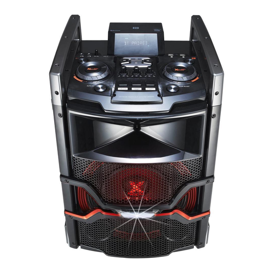
- Page 1 Internal Use Only Website http://biz.lgservice.com Mini Hi-Fi System SERVICE MANUAL MODEL: OM5541 CAUTION BEFORE SERVICING THE UNIT, READ THE “SAFETY PRECAUTIONS” IN THIS MANUAL. P/NO : AFN76793367 SEPTEMBER, 2014...
- Page 2 CONTENTS SECTION 1 ..GENERAL SECTION 2 ..CABINET & MAIN CHASSIS SECTION 3 ..ELECTRICAL SECTION 4 ..REPLACEMENT PARTS LIST...
-
Page 3: Table Of Contents
SECTION 1 SUMMARY CONTENTS ESD PRECAUTIONS ..........................1-3 HIDDEN KEY MODE ........................... 1-4 SERVICE INFORMATION FOR EEPROM ..................1-5 PROGRAM DOWNLOAD & UPDATE GUIDE ................... 1-6 1. MICOM PROGRAM ..........................1-6 2. MCS PROGRAM ............................1-7 3. EQ PROGRAM ............................1-8 SPECIFICATIONS ............................ -
Page 4: Esd Precautions
ESD PRECAUTIONS Electrostatically Sensitive Devices (ESD) Some semiconductor (solid state) devices can be damaged easily by static electricity. Such components commonly are called Electrostatically Sensitive Devices (ESD). Examples of typical ESD devices are integrated circuits and some field-effect transistors and semiconductor chip components. The following techniques should be used to help reduce the incidence of component damage caused by static electricity. -
Page 5: Hidden Key Mode
HIDDEN KEY MODE Push both Front key and RCU key to activate it for 5 seconds. 1. Disc Lock On/Off (CD Function Only Active) Front Key : STOP RCU Key : STOP 2. Check Version and Option code Front Key : STOP RCU Key : PLAY/PAUSE You can change [Audio MCU Version <->... -
Page 6: Service Information For Eeprom
SERVICE INFORMATION FOR EEPROM POWER ON It is possible at any function. FLD “BT READY” status (ex. It is possible at FLD “NO USB” status, too.) This is an example. “ Front STOP” + Remote control “ ” DETECT NEW EEPROM push same timing during 5s (OPTION EDIT SCREEN) NAME... -
Page 7: Program Download & Update Guide
PROGRAM DOWNLOAD & UPDATE GUIDE 1. MICOM PROGRAM Download program file name must be MICOM_OM5541_YYMMDDX.HEX If security program (Water Wall) is activated on your PC, you must save the file to the USB storage device and disable the security software, then download the file to your set. Downloading file proceeds in the same way at USB1 function and USB2 function. -
Page 8: Mcs Program
2. MCS PROGRAM Download program file name must be HG440_OM5541_YYMMDDX.bin If security program (Water Wall) is activated on your PC, you must save the file to the USB storage device and disable the security software, then download the file to your set. Downloading file proceeds in the same way at USB1 function and USB2 function. -
Page 9: Eq Program
3. EQ PROGRAM Download program file name must be EQ_PRG.BIN If security program (Water Wall) is activated on your PC, you must save the file to the USB storage device and disable the security software, then download the file to your set. Downloading file proceeds in the same way at USB1 function and USB2 function. -
Page 10: Specifications
SPECIFICATIONS • GENERAL Power requirements Refer to the main label. Power consumption Refer to the main label. Dimensions (W x H x D) 395.5 mm x 548 mm x 446 mm Net Weight (Approx.) 16.5 kg Operating temperature 5 °C to 35 °C (41 °F to 95 °F) Operating humidity 5 % to 90 % Bus Power Supply (USB) - Page 11 1-10...
- Page 12 SECTION 2 CABINET & MAIN CHASSIS CONTENTS EXPLODED VIEWS ............................. 2-3 1. CABINET AND MAIN FRAME SECTION (OM5541) ................2-3 2. PACKING ACCESSORY SECTION ......................2-5...
- Page 14 EXPLODED VIEWS 1. CABINET AND MAIN FRAME SECTION (OM5541) NOTES) THE EXCLAMATION POINT WITHIN AN EQUILATERAL TRIANGLE IS INTENDED TO ALERT THE SERVICE PERSONNEL TO THE PRESENCE OF IMPORTANT SAFETY INFORMATION IN SERVICE LITERATURE. MAIN SMPS CABLE1 KEY/PTB KEY/USB CABLE2...
- Page 15 2. PACKING ACCESSORY SECTION 801 Instruction Ass'y 825 FM Wire Antenna 808 Battery 900 Remote Control 803 Packing 804 Bag 803 Packing 802 Box...
- Page 16 SECTION 3 ELECTRICAL CONTENTS ONE POINT REPAIR GUIDE ........................3-2 1. NO POWER ............................3-2 2. NO BOOTING WHEN POWER ON THE SET ..................3-4 3. VFD IS NOT DISPLAYED WHEN POWER ON THE SET ..............3-5 4. NO SOUND ............................3-6 ELECTRICAL TROUBLESHOOTING GUIDE ..................
-
Page 17: One Point Repair Guide
ONE POINT REPAIR GUIDE 1. NO POWER If the unit doesn’t work by no power problem, repair the set according to the following guide. (1) FUSE & BRIDGE DIODE [ Solution ] Please check and replace F901, BD901, TH901 or TH903 on SMPS board. [ How to troubleshoot (Countermeasure) ] 1) Check if the fuse F901 is open or short-circuit. - Page 18 ONE POINT REPAIR GUIDE (2) D951 [ Solution ] Please check and replace D951 on SMPS board. [ How to troubleshoot (Countermeasure) ] 1) Check the anode-cathod voltage of D951 with a digital multi-meter, it is normally 0.2 ~ 0.3 V. If it doesn’t have any voltage, it’s destroyed.
-
Page 19: Booting When Power On The Set
ONE POINT REPAIR GUIDE 2. NO BOOTING WHEN POWER ON THE SET The set doesn’t work when press the power button on the front board or the remote control. (1) FLASH MEMORY [ Solution ] Please check and replace IC503 on MAIN board. [ How to troubleshoot (Countermeasure) ] 1) Check 5.6 V to CN501 in standby mode. -
Page 20: Vfd Is Not Displayed When Power On The Set
ONE POINT REPAIR GUIDE 3. VFD IS NOT DISPLAYED WHEN POWER ON THE SET When power on the set, any icons or characters on VFD are not displayed. (1) VFD [ Solution ] Please check and replace DIG400 on FRONT board. [ How to troubleshoot (Countermeasure) ] 1) Check if VKK, FL+ and FL- are output from SMPS to VFD via the MAIN board. -
Page 21: Sound
ONE POINT REPAIR GUIDE 4. NO SOUND There is no sound output by DIGITAL AUDIO AMP DAMAGE, repair the set according to the following guide. (1) BY DIGITAL AUDIO AMP DAMAGE (IN ALL FUNCTIONS) [ Solution ] Please check and replace IC700 on MAIN board. [ How to troubleshoot (Countermeasure) ] 1) Check PWM_FL±... - Page 22 ONE POINT REPAIR GUIDE There is no sound output in the USB FUNCTION, repair the set according to the following guide. (2) IN THE USB FUNCTION [ Solution ] Please check and replace IC501 on MAIN board & IC460 on USB board. [ How to troubleshoot (Countermeasure) ] 1) Check +5 V_USB to USB board.
- Page 23 ONE POINT REPAIR GUIDE There is no sound output in the AUX FUNCTION, repair the set according to the following guide. (3) IN THE AUX FUNCTION [ Solution ] Please check and replace IC201 on MAIN board. [ How to troubleshoot (Countermeasure) ] 1) Check AUX_L/R signals to IC201 (Pin23, 24).
- Page 24 ONE POINT REPAIR GUIDE There is no sound output in the TUNER FUNCTION, repair the set according to the following guide. (4) IN THE TUNER FUNCTION [ Solution ] Please check and replace IC201, TU500 on MAIN board. [ How to troubleshoot (Countermeasure) ] 1) Check if TUNER_LR is entered from Pin1, 3 of TU500 to IC201(Pin26, 27).
- Page 25 ONE POINT REPAIR GUIDE There is no sound output in the PORTABLE FUNCTION, repair the set according to the following guide. (5) IN THE PORTABLE FUNCTION [ Solution ] Please check and replace IC201 on MAIN board. [ How to troubleshoot (Countermeasure) ] 1) Check PT_L/R signals to IC201 (Pin9, 10).
- Page 26 ONE POINT REPAIR GUIDE There is no sound output in the MIC FUNCTION, repair the set according to the following guide. (6) IN THE MIC FUNCTION [ Solution ] Please check and replace IC203 on MAIN board and IC420 on front MIC board. [ How to troubleshoot (Countermeasure) ] 1) Check MIC_SIG signal, from JACK421, JACK422 to IC420 (Pin3) on front MIC board.
-
Page 27: Electrical Troubleshooting Guide
ELECTRICAL TROUBLESHOOTIHG GUIDE 1. POWER (SMPS) No 5.6 VA F901 normal? Replace F901 (Use the same fuse). BD901 normal? Replace BD901. TH901(TH903) normal? Replace TH901. Is Vcc (10 V ~ 18 V) supplied to D902 normal? IC901 Pin7? Check or replace D902. D933 / D934 normal? Replace D933 / D934. - Page 28 ELECTRICAL TROUBLESHOOTIHG GUIDE No PVDD F901 normal? Replace F901 (Use the same fuse). BD901 normal? Replace BD901. TH901(TH903) normal? Replace TH901. Is Vcc (10 V ~ 18 V) supplied to D903 normal? IC911 Pin4? Check or replace D903. Q911 base "H"? •...
- Page 29 ELECTRICAL TROUBLESHOOTIHG GUIDE No 12 V Is Vcc (15 V) Check or replace D935. supplied to IC931? IC931 Pin4 “H”? Check the ‘P.CTL “H”’ signal from μ-com Check or replace IC931. No VFD Check or replace D931. D931 normal? Check or replace ZD931. ZD931 normal? Q501 / Q502 normal? Check or replace Q501 / Q502.
-
Page 30: Mcs Part Check
ELECTRICAL TROUBLESHOOTIHG GUIDE 2. MCS PART CHECK MCS PART CHECK Check if Refer to voltage of CN501 Pin7, 8 SMPS troubleshooting. is 5.6 VA. Check if IC510 Check and change IC510. have 3.3 V output. Check if IC508 Check and change IC508. have 1.2 V output. -
Page 31: Double Usb Function
ELECTRICAL TROUBLESHOOTIHG GUIDE 4. DOUBLE USB FUNCTION USB FUNCTION Plug-in usb device. Display “NO USB”. Check USB_5 V. Check CN421. Check USB jack Check USB Display “READ”. (CN461/ CN462). D+/D- Check IC501 Display “NO FILE”. Replace IC501. (Pin U7, U8, A7, A8). Check usb audio fi... -
Page 32: Fld Display Check
ELECTRICAL TROUBLESHOOTIHG GUIDE 5. FLD DISPLAY CHECK FLD DISPLAY CHECK Check CN501 Pin13,14,15 input Refer to SMPS troubleshooting. voltage. Check if both end voltage of FL+, FL- are over 2.9 V VKK : over 25.6 V. Check CN400 connection and power Check CN400 connection. -
Page 33: Pwm Modulation Check
ELECTRICAL TROUBLESHOOTIHG GUIDE 6. PWM MODULATION CHECK PWM MODULATION PART CHECK Check Refer to CN501 Pin7,8 SMPS troubleshooting. (5.6 V) • Check IC601(TAS5548) VDD 3.3 V - Pin9, 14, 35, 50. • Check X601 (12.288 MHz). Check Check X601 X601(12.288 MHz) Replace X601(12.288 MHz). - Page 34 ELECTRICAL TROUBLESHOOTIHG GUIDE Check IC601(TAS5548) Check input data Check each line resistor output. IC601 DATA Pin24 input. PWM wave. Check PWM modulator output FL: Pin48(-), 49(+) Replace IC601. Check IC601. FR: Pin46(-), 47(+). Other output check. 3-19...
-
Page 35: Power Amp Part Check
ELECTRICAL TROUBLESHOOTIHG GUIDE 7. POWER AMP PART CHECK POWER AMP PART CHECK Check CN501 Pin10: 12 V Refer to SMPS troubleshooting. Pin1,2,3: 48 V. Check IC701 Pin25, 26, 55, 56 input voltage. Check IC700 Check each line resistor output voltage. Pin2, 6, 55: 12 V. -
Page 36: Tuner / Aux Function Check
ELECTRICAL TROUBLESHOOTIHG GUIDE 8. TUNER / AUX FUNCTION CHECK FUNCTION CHECK Check IC201 (CS5346) Pin23, 24, Check JK200, TU500. 26, 27 input. Check IC201 Check IC201 Pin5: +3.3 V Check CN501 Pin7, 8: +5.6 V. (CS5346) Pin41 output Pin14: +5 V. data. -
Page 37: Mic Function Check
ELECTRICAL TROUBLESHOOTIHG GUIDE 9. MIC FUNCTION CHECK MIC FUNCTION CHECK Check IC420(S4308) pin3 Check JK421, JK422. input. Check CN501 pin7, 8: +5.6 V. Check Check IC420 Check IC423 IC420(S4308) pin4 pin6: +5 V pin1: +5 V. data output. Replace IC201. Check IC203 Check Check... -
Page 38: Waveforms Of Major Check Point
WAVEFORMS OF MAJOR CHECK POINT 1. SDRAM IC502 Pin38 DATA IC502 Pin53 ADDRESS IC502 Pin35 IC203 Pin19 2. AUDIO PATH DAC_MCLK IC501 Pin D2 DAC_BCK IC501 Pin E1 DAC_LRCK IC501 Pin D1 DAC_DATA IC501 Pin E2 3. USB USB_5V IC501 Pin A8 IC501 Pin A7 3-23... - Page 39 3-24...
-
Page 40: Wiring Diagram
WIRING DIAGRAM MAIN FFC 10P (FR-4 EPOXY 2LAYER) SMPS (CEM-3 ) AMP 2P Wire Harness 7P FFC 29P Wire Harness 12P FCC 10P Wire Harness 4P Wire Harness 12P FFC 29P FCC 10P VFD&IR MIC & PTB Front & KEY 1 Front &... -
Page 41: Block Diagrams
BLOCK DIAGRAMS 1. SYSTEM BLOCK DIAGRAM_1 SDRAM M0 0~15 MCS_LRCK/BCK/ A 00~11 DATA_OUT M12L64164A Main : 0IMMREB004H(M12L64164A) PWM_MUTE TAS5631BPHD Sub : EAN60700802(W9864G6JH) MLC3730 TAS5548DGG PWM_RST S.FLASH SF_CS/SCK/MISO/ 1.2/3.3V PWM_DAT/CLK MOSI W25Q64F 12.288M W BT : EAN62459301 (4MB) AMP_PDN W/O BT : EAN55718402 (1MB) EEPROM AMP_SD/OTW / PROTECT/ CLIP0(FRONT_AGL) SCL/SDA... -
Page 42: System Block Diagram_2
2. SYSTEM BLOCK DIAGRAM_2 MAIN + AMP PCB PVDD(48V)/GVDD(12V) Key_3 3.3V 3.3V Mic L/R DAC_MCLK / BCK Volume cont I/O U-COM / LRCK / DAC_DATA LC87FC096AVU TAS5548 TAS5631B Tuner 3.3V TUNER 3.3V/1.2V (AM/FM) AMP_SD/OTW / PROTECT/ CLIP0 3.3/5V 24 MHz 32.768 KHz TUNER L/R FRONT1 PCB... -
Page 43: Smps Block Diagram_1
3. SMPS BLOCK DIAGRAM_1 25mA IC400 370mA STBY MC3401 ± VFD DRV 20mA UBS2.0_OTG_VBUS (MLC3730) FRONT2 FRONT B’ d USB PWR 1.4A LM37102D +5.6VA TU500 IC601 IC501 RF IC TUNER DRV_VBUS2.0 u- COM TAS5548 2.2~ 2.6A YST996 IC507 DVCC_3.3V 40mA 160mA 25mA 10mA?? -
Page 44: Smps Block Diagram_2
4. SMPS BLOCK DIAGRAM_2 Snubber Block CN901 Main 12V LDO 12 V SMPS IC Block On/Off 5.6 VA Noise Y-Cap Feedback Filter Photo coupler Block (X-cap P.CTL Y-Cap Photo coupler On/Off Line Filter) Snubber Block PVDD SMPS IC With FET Block Feedback Photo coupler... -
Page 45: Circuit Diagrams
MODIFIED OR ALTERED WITHOUT PERMISSION IMPLEMENTATION OF THE LATEST SAFETY AND during Play mode. FROM THE LG CORPORATION. ALL COMPONENTS PERFORMANCE IMPROVEMENT CHANGES INTO SHOULD BE REPLACED ONLY WITH TYPES IDENTICAL THE SET IS NOT DELAYED UNTIL THE NEW SERVICE TO THOSE IN THE ORIGINAL CIRCUIT. -
Page 46: Main_Dsp Circuit Diagram
2. MAIN_DSP CIRCUIT DIAGRAM MAIN_DSP EAX65685802-SD(#01)_Rev2_1.0 2014. 07. 16 3-37 3-38... -
Page 47: Main_Adc/Pwm Circuit Diagram
3. MAIN_ADC/PWM CIRCUIT DIAGRAM MAIN_ADC/PWM EAX65685802-SD(#02)_Rev2_1.0 2014. 07. 16 3-39 3-40... -
Page 48: Main_Amp Circuit Diagram
4. MAIN_AMP CIRCUIT DIAGRAM MAIN_AMP EAX65685802-SD(#03)_Rev2_1.0 2014. 07. 16 3-41 3-42... -
Page 49: Front_Key/Usb Circuit Diagram
5. FRONT_KEY/USB CIRCUIT DIAGRAM FRONT_KEY/USB EAX65667301-SD_Rev20_1.8 2014. 07. 16 3-43 3-44... -
Page 50: Front_Vfd Circuit Diagram
6. FRONT_VFD CIRCUIT DIAGRAM FRONT_VFD EAX65668701-SD_Rev20_1.8 2014. 07. 16 3-45 3-46... -
Page 51: Front_Key/Ptb Circuit Diagram
7. FRONT_KEY/PTB CIRCUIT DIAGRAM FRONT_KEY/PTB EAX65689401-SD_Rev20_1.9 2014. 07. 16 3-47 3-48... -
Page 52: Front_Mic Circuit Diagram
8. FRONT_MIC CIRCUIT DIAGRAM FRONT_MIC EAX65689601-SD_Rev20_1.8 2014. 07. 16 3-49 3-50... -
Page 53: Spk_Led Circuit Diagram
9. SPK_LED CIRCUIT DIAGRAM SPK_LED EAX64282901_SD_Rev1_1 2014. 07. 16 3-51 3-52... -
Page 54: X_Led/Rcu2 Circuit Diagram
10. X_LED/RCU2 CIRCUIT DIAGRAM X_LED/RCU2 EAX65632101-SD_Rev5_1.3 2014. 07. 16 3-53 3-54... -
Page 55: Circuit Voltage Chart
CIRCUIT VOLTAGE CHART 1. ICs 2. CAPACITORS Designator Description Polarity(+) Polarity(-) REAL CHECK Designator PIN Number Description Part Site Specifi cation SPEC VALUE LOC. OM5540 FRONT IC,Microcontrollers C460 Capacitor,Ceramic,Chip 5.57 Supply Voltage(VDD) 3.10~3.50 3.28 L108 IC101 R5F100GHAFB C462 Capacitor,Ceramic,Chip 5.11 6,35,46 Core Supply Voltage(VDD) 3.13~3.46... -
Page 56: Connectors
3. CONNECTORS PIN NAME Output Voltage SPEC PIN NAME Output Voltage SPEC PIN NAME Output Voltage SPEC CN400 12 V 12.19 11.4 ~ 12.6 -18.11 PWR-CTRL 2.23 3.1 ~ 3.4 -20.77 DGND CN507 -23.42 -23.54 -23 ~ -29 12 V 12,19 DGND -20.84... -
Page 57: Printed Circuit Board Diagrams
PRINTED CIRCUIT BOARD DIAGRAMS 1. SMPS P.C.BOARD (TOP VIEW) (BOTTOM VIEW) NOTE) Warning Parts that are critical with respect to risk of fire or electrical shock. 3-59 3-60... -
Page 58: Main P.c.board
2. MAIN P.C.BOARD (TOP VIEW) (BOTTOM VIEW) 3-61 3-62... -
Page 59: Front_Key/Usb P.c.board
3. FRONT_KEY/USB P.C.BOARD (TOP VIEW) (BOTTOM VIEW) 4. FRONT_VFD P.C.BOARD (TOP VIEW) (BOTTOM VIEW) 3-63 3-64... -
Page 60: Front_Key/Ptb P.c.board
5. FRONT_KEY/PTB P.C.BOARD (TOP VIEW) (BOTTOM VIEW) 6. FRONT_MIC P.C.BOARD (TOP VIEW) (BOTTOM VIEW) 3-65 3-66... -
Page 61: Spk_Led P.c.board
7. SPK_LED P.C.BOARD (TOP VIEW) (BOTTOM VIEW) 8. X_LED/RCU2 P.C.BOARD (TOP VIEW) (BOTTOM VIEW) 3-67 3-68...