Table of Contents
Advertisement
Quick Links
Feb.2003
TABLE OF CONTENTS
SPECIFICATIONS............................................................. 2
LOCATION OF CONTROLS .......................................... 4
LOCATION OF CONTROLS PARTS LIST ................... 4
EXPLODED VIEW ............................................................ 6
EXPLODED VIEW PARTS LIST ..................................... 8
PARTS LIST...................................................................... 10
CHECKING THE VERSION NUMBER....................... 13
Copyright © 2003 ROLAND CORPORATION
All rights reserved. No part of this publication may be reproduced in any form without the written permission
of ROLAND CORPORATION.
RESTORING THE FACTORY SETTINGS................... 13
TEST MODE..................................................................... 13
BLOCK DIAGRAM......................................................... 20
CIRCUIT BOARD............................................................ 22
CIRCUIT BOARD............................................................ 24
CIRCUIT DIAGRAM...................................................... 26
17058813E0
SERVICE NOTES
Issued by RJA
Printed in Japan (0800) (AS)
ME-50
Advertisement
Table of Contents

Related Manuals for Roland Boss ME-50


Summary of Contents for Roland Boss ME-50
-
Page 1: Table Of Contents
CIRCUIT BOARD............24 PARTS LIST..............10 CIRCUIT DIAGRAM............26 CHECKING THE VERSION NUMBER....... 13 Copyright © 2003 ROLAND CORPORATION All rights reserved. No part of this publication may be reproduced in any form without the written permission of ROLAND CORPORATION. 17058813E0... -
Page 2: Specifications
Delay AF method (Adaptive Focus method) Reverb This is a proprietary method from Roland that vastly improves the signal-to- Noise Suppressor noise (S/N) ratio of the A/D and D/A converters. (Effects for Expression Pedal) - Page 3 ME-50...
-
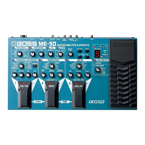
Page 4: Location Of Controls
Feb.2003 ME-50 LOCATION OF CONTROLS fig.panel 17,18 15,16 5,6,18 11,4 LOCATION OF CONTROLS PARTS LIST PART CODE PART NAME DESCRIPTION G2047001 7SEG COVER PART CODE PART NAME DESCRIPTION F5029408 A-601H 1502928100 LED (RED) L-34HDSL G247751301 VGA KEYTOP S WITHOUT LENS F3279803 POTENTIOMETER 11 CLICKS 50KB RD901-40-125F-B54-11D... -
Page 5: Exploded View
Feb.2003 EXPLODED VIEW fig.explo1... - Page 6 ME-50 fig.explo2...
-
Page 7: Exploded View Parts List
Feb.2003 EXPLODED VIEW PARTS LIST [PARTS] PART CODE PART NAME DESCRIPTION G2027904 TOP COVER G2187193 BOTTOM COVER G1147002 REAR PANEL G2047001 7SEG COVER G2187547 VR PEDAL G2187910 PEDAL HOLDER G2147119 BOLT HOLDER G2357125 PEDAL PLATE G2357122 REAR CUSHION G2357111 CUSHION R G2147806 STAY G2217733... - Page 8 ME-50...
-
Page 9: Parts List
Feb.2003 PARTS LIST fig.part1e CONSIDERATION ON PARTS ORDRING SAFETY PRECAUTIONS: When ordering any parts listed in the parts list, please specify the following items in the order sheet. The parts marked have PART NUMBER DESCRIPTION MODEL NUMBER safety-related characteristics. Use 22575241 Sharp Key C-20/50... - Page 10 ME-50 DIODE 1502928100 L-34HDSL LED (RED) LED2,3,6,79,10,11,12,13,14,15,16,17,19,20,21 15029106 LD002VB LED4,8 F5029408 A-601H LED5 F5029117 L-312LRD LED18 15339119 1SS-352 DIODE D1,3,5,6 F5339137 SS14 VF=0.45V DIODE D4,7 RESISTOR F5419707 CRN34101J RESISTOR ARRAY RA1,2,3,4,6 F5419705 CRN34103J RESISTOR ARRAY RA7,9 F5419726 CRN34473J RESISTOR ARRAY RA8,10,11 F5429366 15K OHM F RANK (1%)
- Page 11 Feb.2003 WIRING,CABLE F3467025 WIRING 2P F3467024 WIRING 3P SCREWS H5039111 WASHER D8D3T0.5 H5039515 NUT M6 U BZC H5019124 SCREW M3X6 PAN MACHINE W/SW+SMALL PW ZC H5019130 SCREW M3X6 PAN MACHINE W/SW+PW ZC H5039121 WASHER 9.5X6.5 HSJ-0999-01-210 H5039514 NUT M6 HSJ-0999-01-190 H5029867 HEX BOLT M6X70 HALF THEREAD BZ...
-
Page 12: Checking The Version Number
ME-50 CHECKING THE VERSION Noise Meter NUMBER Filter: IHF-A (JIS-A) Foot Switch (FS-5U) • Device Settings Turn the VR knobs (pots) completely to the left (minimum). POLARITY SW: Jack • Hold down the [EDIT/EXIT] switch and [WRITE] switch and turn the POWER switch on. - Page 13 Feb.2003 fig.test-3_50 fig.test-6_50 5 6 7 8 9 • With all LEDs lit, press the following switches to enable selection of the type of check to start. Press the [FOOT 1] switch to proceed to the “Version Check.” If no problem exists, the procedure automatically proceeds to the next step. Press the [FOOT 2] switch to proceed to “5.
- Page 14 ME-50 [PEDAL MODE SW] = “0”--”5” If no problem exists, the procedure automatically proceeds to the next step. fig.test-10_50 6. EXP Pedal Check • Start with the expression pedal in the depressed position. • Carry out the following operations in the indicated sequence. fig.test-15_70 (2) Non-Notched VR Check 1.
- Page 15 Feb.2003 [Mute Off] [Mute On] fig.test-20_50 fig.test-21_50 • Disconnect the cable from OUTPUT R, then confirm that the waveform [Mute On] output by OUTPUT L(MONO) changes accordingly, as shown in the figures below. fig.test-21_50 [Mute Off] fig.test-20_50 • Next, connect the cable to OUTPUT R, then confirm that the waveform output by OUTPUT R changes accordingly, as shown in the figures below.
- Page 16 ME-50 [Mute On] fig.test-22_50 fig.test-24_50 [Mute On] Press the [ ] switch to proceed to the next step. fig.test-21_50 9. DRAM Check fig.test-25_70 • Oscilloscope Settings: Ch1: 0.2 V/div; Ch2: 0.2 V/div; TIME: 0.5 ms/div • Connect the cable only to the OUTPUT L(MONO) jack, then confirm that the waveform from OUTPUT is smooth, as shown in the figure below.
- Page 17 Feb.2003 fig.test-27_50 fig.test-30_50 • Confirm that the LINE/PHONES waveform amplitude is between 290 • Press the [ ] switch to proceed to the next step. and 410 (mVp-p). 10. INPUT A/D Check, AUX IN Check, Noise Check fig.test-28_70 (1) INPUT A/D Check Input a rectangular wave to the INPUT jack only, then check the waveform from OUTPUT.
- Page 18 ME-50 Note: Release the pedal when the pedal is fully raised, then press the [WRITE] switch. If an error occurs, the green LED in the upper portion of the seven-segment LED display flashes. fig.test-33_70 • Press the unit’s expression pedal completely forward, release the pedal, and press the [WRITE] switch.
-
Page 19: Block Diagram
Feb.2003 ME-50 BLOCK DIAGRAM fig.block JK 1 Pre Emph JK 2 INPUT BUFFER Level CTL OUTPUT R JK 5 DE Emph (MONO) CODEC BUFFER AUX IN Level CTL JK 6 (AD/DA) CTL1,2 IC18 JK 3 OUTPUT L ANALOG MULTIPLEXER VR 2-5 MUTE Q2,3 ANALOG... -
Page 20: Circuit Board
Feb.2003 ME-50 CIRCUIT BOARD comp.eps View from components side... - Page 21 Feb.2003 ME-50 CIRCUIT BOARD foil.eps View from foil side...
-
Page 22: Circuit Diagram
Feb.2003 ME-50 CIRCUIT DIAGRAM fig.main-cr 0.0022 N.I.U. R126 10k GUITAR INPUT 10/16 2SK880GR 0.0022 C128 100/16 N.I.U. R127 0.47S R5 10k 10/16 5.6k OUTPUT R IC2A EXP BOARD NJM2100M HTJ-064-12I IC1A C133 10/16 M5218AFP N.I.U. IC18A 10/16 10/16 M5218AFP EXP PEDAL AVCC 10/16 150k(F)