Table of Contents
Advertisement
Technical Supplement
©
2003 VERTEX STANDARD CO., LTD.
Specifications .................................................................................................................................................................. 2
Exploded View & Miscellaneous Parts ...................................................................................................................... 4
Connection Diagram ...................................................................................................................................................... 5
Block Diagram ................................................................................................................................................................ 6
Circuit Description ......................................................................................................................................................... 7
Alignment ...................................................................................................................................................................... 11
Board Units (Schematics, Layouts & Parts)
MAIN Unit ................................................................................................................................................................ 17
FILTER Unit .............................................................................................................................................................. 33
SW Unit ..................................................................................................................................................................... 37
VCO Unit .................................................................................................................................................................. 39
EH015M90A
Introduction
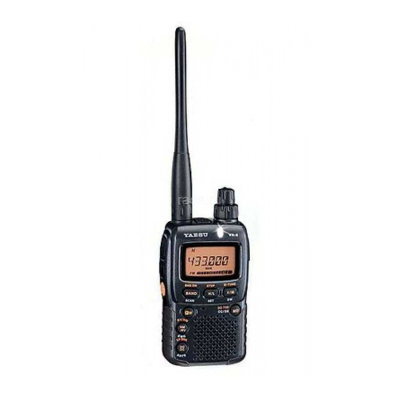
This manual provides the technical information necessary for servicing the VX-2R
VHF/UHF Ultra-Compact Dual-Band Transceiver with Wide Band Coverage.
Servicing this equipment requires expertise in handing surface-mount chip com-
ponents. Attempts by non-qualified persons to service this equipment may result
in permanent damage not covered by the warranty, and may be illegal in some
countries.
Two PCB layout diagrams are provided for each double-sided board in this trans-
ceiver. Each side of the board is referred to by the type of the majority of compo-
nents installed on that side ("Side A" or "Side B"). In most cases one side has only
chip components (surface-mount devices), and the other has either a mixture of
both chip and leaded components (trimmers, coils, electrolytic capacitors, ICs,
etc.), or leaded components only.
As described in the pages to follow, the advanced microprocessor design of the
VX-2R allows a complete alignment of this transceiver to be performed without
opening the case of the radio; all adjustments can be performed from the front
panel, using the "Alignment Mode" menu.
While we believe the information in this manual to be correct, VERTEX STAN-
DARD assumes no liability for damage that may occur as a result of typographical
or other errors that may be present. Your cooperation in pointing out any incon-
sistencies in the technical information would be appreciated.
Contents
VERTEX STANDARD CO., LTD.
4-8-8 Nakameguro, Meguro-Ku, Tokyo 153-8644, Japan
VERTEX STANDARD
US Headquarters
10900 Walker Street, Cypress, CA 90630, U.S.A.
International Division
8350 N.W. 52nd Terrace, Suite 201, Miami, FL 33166, U.S.A.
YAESU EUROPE B.V.
P.O. Box 75525, 1118 ZN Schiphol, The Netherlands
YAESU UK LTD.
Unit 12, Sun Valley Business Park, Winnall Close
Winchester, Hampshire, SO23 0LB, U.K.
VERTEX STANDARD HK LTD.
Unit 5, 20/F., Seaview Centre, 139-141 Hoi Bun Road,
Kwun Tong, Kowloon, Hong Kong
Downloaded by
RadioAmateur.EU
1
Advertisement
Table of Contents

Related Manuals for Yaesu Yaesu VX-2R


Summary of Contents for Yaesu Yaesu VX-2R
-
Page 1: Table Of Contents
Technical Supplement © 2003 VERTEX STANDARD CO., LTD. Specifications ... 2 Exploded View & Miscellaneous Parts ... 4 Connection Diagram ... 5 Block Diagram ... 6 Circuit Description ... 7 Alignment ... 11 Board Units (Schematics, Layouts & Parts) MAIN Unit ... 17 FILTER Unit ... -
Page 2: Specifications
Specifications General Frequency Ranges: (USA Version) Channel Steps: 5/9/10/12.5/15/20/25/50/100 kHz Frequency Stability: ±5 ppm (14 °F to +140 °C [–10 °C to +60 °C]) Repeater Shift: ±600 kHz (144 MHz) ±1.6/5.0/7.6 MHz (430 MHz) Emission Type: F2 , F3 Antenna Impedance: 50 W Supply Voltage: Nominal:3.7 V DC, Negative Ground... - Page 3 Receiver Circuit Type: AM, NFM: Double-Conversion Superheterodyne WFM: Triple-Conversion Superheterodyne Intermediate Frequencies: AM, NFM Sensitivity: 3 µV for 10 dB SN (0.5-30 MHz, AM) 0.35 µV TYP for 12 dB SINAD (30-54 MHz, NFM) 1 µV TYP for 12 dB SINAD (54-76 MHz, NFM) 1.5 µV TYP for 12 dB SINAD (76-108 MHz, WFM) 1.5 µV TYP for 10 dB SN (108-137 MHz, AM) 0.2 µV for 12 dB SINAD (137-140 MHz, NFM)
-
Page 4: Exploded View & Miscellaneous Parts
Exploded View & Miscellaneous Parts RA0111400 RING NUT RA0504400 ENCODER KNOB RA0504300 VOLUME KNOB RUBBER CAP (SP) RUBBER CAP (DC) VXSTD P/N DESCRIPTION • U07125302 PAN HEAD SCREW M1.7X2.5NI#3 ‚ U07180306 PAN HEAD SCREW M1.7X8AU#3 ƒ U07240302 PAN HEAD SCREW M2X4NI#3 „... -
Page 5: Connection Diagram
Connection Diagram Downloaded by RadioAmateur.EU... -
Page 6: Block Diagram
Block Diagram Downloaded by RadioAmateur.EU... -
Page 7: Circuit Description
The VX-2R consists of a MAIN-UNIT, a FILTER-UNIT, a SW-UNIT, and a VCO-UNIT. The MAIN-UNIT contains the receiver front end, IF circuit, PLL circuit, the CPU, audio ICs, and the power circuitry for the LCD. The FIL- TER-UNIT contains the CTCSS/DCS Encoder/Decoder cir- cuit. - Page 8 Circuit Description to varactors D1016 and D1017 (both HVC355B) in the variable frequency band-pass filters. By changing the elec- trostatic capacitance of the varactors, optimum filter char- acteristics are provided for each specific operating fre- quency. ( 6 ) 47.25-MHz First Intermediate Frequency The 47.25-MHz first intermediate frequency from first mixers is delivered to the first IF circuit.
- Page 9 ( 4 ) 435-MHz-Band Transmission Modulating audio passes through deviation setting D/A converter Q1010 (M62364FP) then delivered to the UHF modulator of the VCO-UNIT mounted on the MAIN- UNIT. This signal is applied to varactor D4002 (HSC277) in the tank circuit of UHF VCO Q4002 (EC3H07B), which oscillates at the desired UHF transmitting frequency.
- Page 10 Circuit Description Note...
-
Page 11: Alignment
We recommend that servicing be performed only by au- thorized Vertex Standard service technicians who are ex- perienced with the circuitry and fully equipped for re- pair and alignment. If a fault is suspected, contact the deal- er from whom the transceiver was purchased for instruc- tions regarding repair. - Page 12 Alignment Internal System Alignment Routine This process uses a programmed routine in the transceiv- er which simplifies many previously complex discrete component settings and adjustments with digitally-con- trolled settings via front panel keys and LCD indications. Set the transceiver to the 430MHz band, then turn the transceiver off.
- Page 13 TX Low Power (Low Band Edge) Adjustment (LP) r Press the [ V/M ] key. r Transmit, and adjust the output power level for 0.1 W (±0.05 W) by rotating the DIAL knob, then press the [ V/M ] key. r Rotate the DIAL knob to select the next setting.
- Page 14 Alignment CTCSS Tone (254.1 Hz) Deviation (High Band Edge) r Press the [ V/M ] key. r Transmit, and adjust the deviation for ±0.6 kHz (±0.05 kHz) by rotating the DIAL knob, then press the [ V/M ] key. r Rotate the DIAL knob to select the next setting. DCS Tone Deviation (High Band Edge) Adjustment (dCS) r Press the [ V/M ] key.
- Page 15 Wide FM Low-Scale S-1 Adjustment (S1) r Press the [ V/M ] key. r Adjust the generator level to 0 dBµ (1 kHz tone @ ±20 kHz deviation), then press the [ F/W ] key. r Press the [ F/W ] key again, then press the [ V/M ] key. r Rotate the DIAL knob to select the next setting.
- Page 16 Alignment TX Deviation (High Band Edge) Adjustment (dEV) r Press the [ V/M ] key. r Inject a 1 kHz audio tone at a level of 50 mV (rms) to the MIC jack, then press the [ F/W ] key. r Transmit, and adjust the deviation for 4.2 kHz (±0.2 kHz) by rotating the DIAL knob, then press the [ V/M ] key.
-
Page 17: Main Unit
850.1 MHz NFM: +8.7 dBµ 47.25 MHz NFM: +4.0 dBµ 0.001 µF Coupling Capacitor 0.01 µF Coupling Capacitor 1.9 V 0.9 V 1.9 V 0.7 V 0.8 V 439.1 MHz NFM: -4.9 dBµ 2.3 V 0.001 µF Coupling Capacitor 0.7 V 2.5 V 2.2 V WFM: 2.7 V... - Page 18 MAIN Unit...
- Page 19 HD64F2266TF13 AT24C256N NJM12904R (Q1076) (Q1080) (Q1082) 2SJ364 (4M) 2SA1774 (FR) 2SC4617 (BR) (Q1044, 1053) (Q1046, 1050, 1057, (Q1011, 1019, 1045, 1070) 1062, 1071, 1075) 2SC5227 (Q1002, 1012) 2SC5374 (NA) (Q1065) 2SC5555 (ZD-) (Q1009, 1015) DTC144EM (26) EMB3 (B3) (Q1003, 1038, 1043, (Q1037, 1047, 1048, 1052, 1072, 1074, 1051, 1058)
- Page 20 MAIN Unit Parts Layout (Side B) M62364FP MB15A01PFV1 (Q1010) (Q1034) TA31136FN (Q1033) 2SA1774 (FR) 2SC4617 (BR) (Q1027, 1032) (Q1040, 1041, 1042) 2SC4915 (QY) (Q1017, 1020, 1021, 1022, 1023, 1028, 1035) 2SC5374 (NA) (Q1024, 1025, 1026) 2SC5555 (ZD-) (Q1004, 1005, 1008, 1013, 1014) EMG2 (G2) (Q1018, 1030)
-
Page 21: Parts List
DESCRIPTION VALUE PCB with Components Printed Circuit Board C 1001 CHIP CAP. C 1002 CHIP CAP. C 1003 CHIP CAP. 10pF C 1004 CHIP CAP. 0.001uF C 1005 CHIP CAP. 33pF C 1006 CHIP CAP. 56pF C 1007 CHIP CAP. 0.001uF C 1008 CHIP CAP. - Page 22 MAIN Unit Parts List DESCRIPTION VALUE C 1073 CHIP CAP. 0.5pF C 1074 CHIP CAP. 33pF C 1075 CHIP CAP. C 1076 CHIP CAP. C 1078 CHIP CAP. 33pF C 1079 CHIP CAP. 22pF C 1080 CHIP CAP. 0.001uF C 1081 CHIP CAP.
- Page 23 DESCRIPTION VALUE C 1149 CHIP CAP. 0.047uF C 1150 CHIP CAP. 100pF C 1151 CHIP CAP. 0.1uF C 1152 CHIP TA.CAP. 22uF C 1153 CHIP CAP. 0.01uF C 1154 CHIP CAP. 0.01uF C 1155 CHIP CAP. 0.01uF C 1156 CHIP CAP. 100pF C 1157 CHIP CAP.
- Page 24 MAIN Unit Parts List DESCRIPTION VALUE C 1225 CHIP TA.CAP. 22uF C 1226 CHIP CAP. 0.1uF C 1227 CHIP CAP. 15pF C 1228 CHIP CAP. 0.001uF C 1229 CHIP CAP. C 1230 CHIP CAP. C 1231 CHIP CAP. 0.001uF C 1233 CHIP TA.CAP.
- Page 25 DESCRIPTION VALUE C 1303 CHIP CAP. 0.01uF C 1304 AL.ELECTRO.CAP. C 1305 CHIP CAP. 0.022uF C 1306 CHIP CAP. C 1307 CHIP CAP. 0.001uF C 1308 CHIP CAP. 0.001uF C 1309 CHIP TA.CAP. C 1310 CHIP CAP. 0.001uF C 1311 CHIP TA.CAP.
- Page 26 MAIN Unit Parts List DESCRIPTION VALUE D 1036 DIODE D 1037 DIODE D 1038 DIODE D 1039 DIODE D 1040 DIODE D 1041 DIODE D 1042 DIODE D 1043 DIODE D 1044 DIODE D 1045 DIODE D 1046 DIODE D 1047 DIODE D 1048 DIODE...
- Page 27 DESCRIPTION VALUE L 1015 M.RFC 0.0056uH L 1016 M.RFC 0.01uH L 1017 M.RFC 0.01uH L 1018 M.RFC 0.082uH L 1019 M.RFC 0.082uH L 1020 M.RFC 0.1uH L 1021 M.RFC 0.1uH L 1022 M.RFC 33uH L 1024 M.RFC 0.01uH L 1025 M.RFC 0.082uH L 1026...
- Page 28 G3117748R G3346178R G3070309 G3070301 G3070309 G3346178R ø G1093814 G3070223 G1092438 G1093837 G3070277 G1093337 G1092215 G3070309 J24189033 J24189031 J24189025 J24189025 J24189025 J24189017 J24189013 J24189025 J24189045 J24189049 J24189031 J24189017 J24189017 J24189045 J24189017 J24189025 J24189033 J24189021 J24189049 ø : Please contact Vertex Standard...
- Page 29 DESCRIPTION VALUE R 1020 CHIP RES. R 1021 CHIP RES. R 1022 CHIP RES. R 1023 CHIP RES. R 1024 CHIP RES. R 1025 CHIP RES. R 1026 CHIP RES. R 1027 CHIP RES. R 1028 CHIP RES. R 1029 CHIP RES.
- Page 30 MAIN Unit Parts List DESCRIPTION VALUE R 1095 CHIP RES. R 1096 CHIP RES. R 1097 CHIP RES. R 1098 CHIP RES. R 1099 CHIP RES. R 1100 CHIP RES. R 1101 CHIP RES. 4.7k R 1102 CHIP RES. 470k R 1103 CHIP RES.
- Page 31 DESCRIPTION VALUE R 1170 CHIP RES. 4.7k R 1171 CHIP RES. 3.3k R 1172 CHIP RES. 2.2k R 1173 CHIP RES. R 1174 CHIP RES. R 1175 CHIP RES. R 1176 CHIP RES. 330k R 1177 CHIP RES. R 1178 CHIP RES.
- Page 32 MAIN Unit Parts List DESCRIPTION VALUE R 1246 CHIP RES. 330k R 1247 CHIP RES. 100k R 1248 CHIP RES. R 1249 CHIP RES. R 1250 CARBON FILM RES. 100k S 1008 ROTARY ENCODER TH1001 THERMISTOR TH1002 THERMISTOR X 1001 XTAL TSS-6 11.7MHz X 1002...
-
Page 33: Filter Unit
3.0 V 1.2 V 1.3 V 1.3 V 1.2 V TONE SQL, DCS: 0 V WX CH SCAN: 2.5 V 0.6 V 0.8 V 1.0 V TONE FREQUENCY ~ 146.2 Hz: 2.5 V 151.4 Hz ~ : 0 V Filter Unit Circuit Diagram 0.6 V 1.2 V... - Page 34 Filter Unit Parts Layout NJM2904R (Side A) 2SC4154 (LE) (Q2003, 2006) DA221M (K) (Side B) NJM12902V (Q2002) (Q2001) DTC144EE (LE) (Q2004, 2005, 2007, 2008) DAN222M (N) (D2002) (D2001)
- Page 35 DESCRIPTION VALUE PCB with Components Printed Circuit Board C 2001 CHIP CAP. C 2002 CHIP CAP. 0.0047uF C 2003 CHIP CAP. 0.0047uF C 2004 CHIP TA.CAP. 4.7uF C 2005 CHIP CAP. 0.01uF C 2006 CHIP CAP. 0.0027uF C 2007 CHIP CAP. 0.022uF C 2008 CHIP CAP.
- Page 36 Filter Unit Note...
-
Page 37: Sw Unit
146 MHz TX: 3.3 V 146 MHz TX: 1.6 V 440 MHz TX: 3.7 V 440 MHz TX: 1.9 V TX: 0.8 V TX: 0.8 V 2SK3079A (E23) 2SC5226 (R22) (Q3002) (Q3001) 2SC5374 (NA) (Q3004) DTC143ZE (E23) (Q3003) RX: 0.4 V 146 MHz TX: 1.6 V 440 MHz TX: 1.3 V RX: 4.1 V... - Page 38 SW Unit Parts List DESCRIPTION VALUE PCB with Components Printed Circuit Board C 3002 CHIP CAP. 33pF C 3003 CHIP CAP. 27pF C 3006 CHIP CAP. 0.001uF C 3007 CHIP CAP. 0.001uF C 3008 CHIP CAP. 33pF C 3009 CHIP CAP. 0.1uF C 3010 CHIP CAP.
-
Page 39: Vco Unit
VCO Unit Circuit Diagram Downloaded by RadioAmateur.EU... - Page 40 VCO Unit Parts Layout (Side A) (Side B) DTC143ZE (E23) (Q4001, 4003, 4007) EC3H07B (G) (Q4002, 4004, 4005, 4006)
- Page 41 DESCRIPTION VALUE PCB with Components Printed Circuit Board C 4001 CHIP CAP. 0.001uF C 4002 CHIP CAP. 0.01uF C 4003 CHIP CAP. 0.5pF C 4004 CHIP CAP. 0.01uF C 4005 CHIP CAP. 0.01uF C 4006 CHIP CAP. C 4007 CHIP CAP. 0.01uF C 4008 CHIP CAP.
- Page 42 VCO Unit Parts List DESCRIPTION VALUE L 4011 M.RFC L 4012 M.RFC 0.33uH L 4013 M.RFC 0.033uH L 4014 M.RFC 0.1uH L 4015 M.RFC 0.22uH Q 4001 TRANSISTOR Q 4002 TRANSISTOR Q 4003 TRANSISTOR Q 4004 TRANSISTOR Q 4005 TRANSISTOR Q 4006 TRANSISTOR Q 4007...
- Page 44 Copyright 2003 VERTEX STANDARD CO., LTD. All rights reserved No portion of this manual Downloaded by may be reproduced without RadioAmateur.EU the permission of VERTEX STANDARD CO., LTD.