Table of Contents
Advertisement
Quick Links
Service Manual
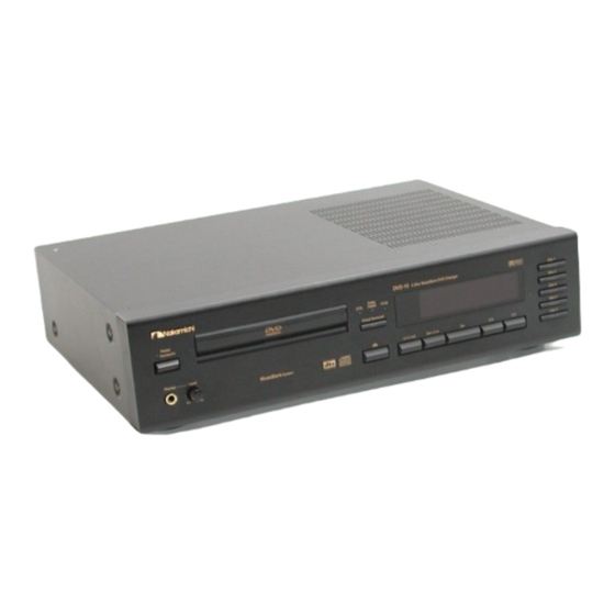
5 Disc MusicBank DVD Changer
CONTENTS
1. GENERAL .............................................................................................................................. 2
2. REMOVAL PROCEDURES .................................................................................................... 4
3. ELECTRICAL ADJUSTMENT ............................................................................................... 9
3-1 Measurement instruments and jigs .................................................................................. 9
3-2 Parts location for adjustment ............................................................................................ 9
3-3 Adjustment Procedure .................................................................................................... 10
3-4 RAM Clear ...................................................................................................................... 11
4. MECHANICAL ASS'Y AND PARTS LIST ........................................................................... 12
4-1 Synthesis Ass'y .............................................................................................................. 12
4-2 Mechanism Ass'y DVD-15 (A01) ................................................................................... 14
4-3 Motor Chassis EX Ass'y (B01) ....................................................................................... 16
4-4 Loading EX Ass'y ADJ-3 (B02) ..................................................................................... 17
4-5 DVD Traverse Ass'y ADJ-3 (B03) ................................................................................... 19
4-6 Pakage Ass'y and Accessory Ass'y ............................................................................... 20
5. ELECTRICAL PARTS LIST ................................................................................................. 21
6. RECOMMENDED SPARE PARTS LIST .............................................................................. 26
7. IC BLOCK DIAGRAMS ........................................................................................................ 27
8. SPECIFICATIONS ................................................................................................................ 49
For Schematic Diagrams, and Mounting Diagrams, see the separate volume.
DVD-15
1
R
Advertisement
Table of Contents

Related Manuals for Nakamichi DVD-15


Summary of Contents for Nakamichi DVD-15
- Page 1 3-4 RAM Clear ........................11 4. MECHANICAL ASS’Y AND PARTS LIST ................12 4-1 Synthesis Ass’y ......................12 4-2 Mechanism Ass’y DVD-15 (A01) ................... 14 4-3 Motor Chassis EX Ass’y (B01) ..................16 4-4 Loading EX Ass’y ADJ-3 (B02) ..................17 4-5 DVD Traverse Ass’y ADJ-3 (B03) ...................
-
Page 2: General
1. GENERAL 1.1 Product Code OBSERVERA! Sådana inställningar av rattarna, omkopplarna eller V685 övriga kontrollknappar som inte är beskriva i 1.2 Destinations bruksanvisningen kan resultera i farlig laserutstrålning. BS, CAN, CH, DA, EP, HK, JPN, OTR, TW, USA, Justering eller reparation av denna kompaktskivspelare KR, AUS skall endast utföras av kvalificerad servicepersonal. - Page 3 GENERAL • How to prevent or discharge the impressed elec- 1.4 Caution for handling Laser Pickup of DVD Player tricity Please refer to the following items. [Electric Influence because of impressed electricity] Laser pickup of a DVD player is weaker and more sen- 1) Grounding sitive than that of CD player, it is possible to damage When you repair a laser pickup, first ground the human...
-
Page 4: Removal Procedures
2. REMOVAL PROCEDURES • Location of Major Parts DVD Main P.C.B. Ass'y Digital P.C.B. Ass'y (Bottom side of Mechanism BLK P-Supply P.C.B. Ass'y Output P.C.B. Ass'y Mechanism BLK Ass'y REG 5V P.C.B. Ass'y LED P.C.B. Ass'y H.P P.C.B. Ass'y REG 3V P.C.B. Ass'y Power-SW P.C.B. - Page 5 REMOVAL PROCEDURES P-Supply P.C.B. Ass'y 2.2 Front Panel (Refer to Fig. 2-3) H.P P.C.B. Ass'y 1) Remove the 5 screws on the front panel. Digital 2) Remove the screws holding the H.P P.C.B. Ass’y. The screws P.C.B. Ass'y can be reached by going through the hole in the left side Power-SW P.C.B.
- Page 6 REMOVAL PROCEDURES 2.6. Bottom Cover EX Ass'y, Top Cover EX Ass'y 6) Pull the edges of the connector CN200 "8" on the Mecha- and F Panel EX Ass'y (Refer to Fig. 2-7) nism P.C.B. Ass'y to unlock the connector edges and care- 1) Remove the 6 screws "1"...
- Page 7 REMOVAL PROCEDURES 2.6. Top Cover EX Ass'y 2.8. Loading EX Ass'y 2.9. DVD Traverse Ass'y 2.7. Mechanism P.C.B. Ass'y 2.6. Panel EX Ass'y 2.6. Bottom Cover EX Ass'y Fig.2-7...
- Page 8 REMOVAL PROCEDURES 2.10 Pickup 1) Remove the DVD Traverse Ass’y. Refer to item 2.9. (Refer to Fig.2-8) 2) Remove a screw F01 (M1.7x3.5+Pan CMT) and detach F02 Caution: Do not remove or loosen screws that are not in- (Hook L.S) cluded in this procedure.
-
Page 9: Measurement Instruments And Jigs
3. ELECTRICAL ADJUSTMENT 3.1 Measurement instruments and Jigs 1) DC Voltmeter 2) AC Voltmeter 3) Tracking Offset Meter LE-9055A or LTM-9055 (Leader Electronics Corp.) 4) A-BEX Vertical Deviation Test Disc TDV-562 (DA09206A) 5) SONY Test Disc Type 3 3.2 Parts Location for Adjustment Fig.3-1 Parts Location for Electorical Adjustment (DVD Main P.C.B. -
Page 10: Adjustment Procedure
ELECTRICAL ADJUSTMENT 3.3 Adjustment procedure (Follow the next steps in order) SIGNAL OUTPUT ITEM ADJUSTMENT REMARKS STEP SOURCE CONNECTION 1. Connect each measuring instrument as follows: DVD Adjust • Connect a DC voltmeter between TP120 (AS) (+ terminal) Mode and TP107 (VREF) (- terminal) on the DVD Main P.C.B. Ass’y. •... -
Page 11: Ram Clear
ELECTRICAL ADJUSTMENT SIGNAL OUTPUT ITEM STEP ADJUSTMENT REMARKS SOURCE CONNECTION CD Tracking CD Test Disc Tracking Offset VR110 1. Set the tracking offset meter as follows: Adjustment SONY Meter • Sensitivity switch: HIGH (right side) • Level switch: MEASURE (left side) Type 3 between •... -
Page 12: Mechanical Ass'y And Parts List
4. MECHANICAL ASS’Y AND PARTS LIST 4.1 Synthesis Ass’y Fig.4-1... - Page 13 DIODE P.C.B. Ass’y 0H08596C Display Lens BK10557A REG.3V P.C.B. Ass’y 0H08585E Front Panel BK BK10556A REG.5V P.C.B. Ass’y (USA/CAN/UK/EP/AUS/DA) ----------- MECHANISM Ass’y DVD-15 0H08586D Dress Panel CG 0E03032A BT4x8+Washer Faced (Black) (CH/JPN/OTR/HK/KR/TW) (USA/CAN/UK/EP/AUS/DA) BK10268A POW SW P.C.B. Ass’y 0E04146A BT4x8+Pan Flange BK10257A LED P.C.B.
-
Page 14: Mechanism Ass'y Dvd-15 (A01)
MECHANICAL ASS’Y AND PARTS LIST 4.2 Mechanism Ass’y DVD-15 (A01) Fig.4-2... - Page 15 MECHANICAL ASS’Y AND PARTS LIST We suggest that you use grease FL-955/G-4270 or equiva- 4.2 Mechanism Ass’y DVD-15 (A01) lent type. Ref. No. Part No. Description Q'ty The company dealing FL-955/G-4270 is as follows: • FL-955 : Kanto Chemicals Co., Ltd.
-
Page 16: Motor Chassis Ex Ass'y (B01)
MECHANICAL ASS’Y AND PARTS LIST 4.3 Motor Chassis EX Ass’y (B01) Fig.4-3 4.3 Motor Chassis EX Ass’y (B01) Ref. No. Part No. Description Q'ty CA09415A Motor Chassis EX Ass’y Apply FL-955 (grease) to the following places (marked 0C10238A Loading Plate Cam SL with ★... -
Page 17: Loading Ex Ass'y Adj-3 (B02)
MECHANICAL ASS’Y AND PARTS LIST 4.4 Loading EX Ass’y ADJ-3 (B02) Fig.4-4... - Page 18 MECHANICAL ASS’Y AND PARTS LIST 4.4 Loading EX Ass’y ADJ-3 (B02) Apply FL-955 (grease) to the following places (marked Ref. No. Part No. Description Q'ty with ★ ) when parts are replaced. CA09505A Loadig EX Ass’y ADJ-3 Ref. No. Location Remarks 0C10201A Loading Plate R SL...
-
Page 19: Dvd Traverse Ass'y Adj-3 (B03)
MECHANICAL ASS’Y AND PARTS LIST 4.5 DVD Traverse Ass’y ADJ-3 (B03) ☆ : Apply lubricant PG-663 Apply PG-663 19: Gear and Gear Top Lubricant: We suggest that you use PG-663 or equivalent type. Please contact: Dowcorning Co., Ltd. 1-1-3 Marunouchi, Chiyoda-ku, Tokyo, Japan Fig.4-5 4.5 DVD Traverse Ass’y ADJ-3 (B03) -
Page 20: Pakage Ass'y And Accessory Ass'y
MECHANICAL ASS’Y AND PARTS LIST 4.6 Pakage Ass’y and Accessory Ass’y Accessory Ass'y Fig.4-6 4.6 Pakage Ass’y and Accessory Ass’y Ref. No. Part No. Description Q'ty Ref. No. Part No. Description Q'ty 0F05622B Carton Box 0D07243A AC Cord CH (CH) 0F05623B Packing 0D07244A... -
Page 21: Electrical Parts List
5. ELECTRICAL PARTS LIST Ref. No. Part No. Description Q'ty Notes: ZD033 0B12168A RD10V JS B2 1. Abbreviations TR-Transistor, SID-Slicon Diode, ZD-Zener Diode, ZD401 0B12150A RD5.6V JS B2 RC-Cement Resistor, RF-Fail Safe Type Resistor, ZD402 0B12160A RD7.5V JS B3 RK-Carbon Resistor. ZD403 0B12153A RD6.2V JS B2... - Page 22 ELECTRICAL PARTS LIST 5.2 DVD Main P.C.B. Ass’y (C3M1) Ref. No. Part No. Description Q'ty Ref. No. Part No. Description Q'ty P800 0B85696A SO 40FLT-SM1-TB* P803 0B85694A FFC 24FLT-SM1-TB* P807 0B85697A SO S06B-XH-SM3-TB* BK10567A DVD Main P.C.B. Ass’y C3M1 P999 0B85695A SO 10FM-1.0-SP1.9* D101,102...
- Page 23 ELECTRICAL PARTS LIST Ref. No. Part No. Description Q'ty 5.3 Digital P.C.B. Ass’y Ref. No. Part No. Description Q'ty P550 0B85930A 14P F Connector* P570 0B85829A 24P F Connector* BK10258A Digital P.C.B. Ass’y (USA/CAN) P600 0B85931A 17P F Connector* BK10562A Digital P.C.B.
- Page 24 ELECTRICAL PARTS LIST 5.4 Output P.C.B. Ass’y Ref. No. Part No. Description Q'ty Ref. No. Part No. Description Q'ty D613,614 0B13385A LED Amber (605NM) SW601,602 0B70298A Tact SW SW603,604 0B70298A Tact SW BK10255A Output P.C.B. Ass’y (Except UK/EP/JPN) SW605,606 0B70298A Tact SW BK10377A Output P.C.B.
- Page 25 ELECTRICAL PARTS LIST 5.14 Mecha Flexible P.C.B. Ass’y 5.8 M-Trans P.C.B. Ass’y Ref. No. Part No. Description Q'ty Ref. No. Part No. Description Q'ty BA09736A Mecha Flexible P.C.B. ASS’y BK10376A M Trans P.C.B. Ass’y D500,501 0B12586A SID 1N4002 PC701,702 0B10737A IC PhotoInterrupter D510,511 0B12586A SID...
- Page 26 6. RECOMMENDED SPARE PARTS LIST Ref. No. Part No. Description Notes: 1. Abbreviations 0B13256A HD6433396F* TR-Transistor, SID-Slicon Diode, ZD-Zener Diode, 0B17033A NJM78M12FA RC-Cement Resistor, RF-Fail Safe Type Resistor, 0B10520A GBU6D RK-Carbon Resistor. 0B10539A MA152WK* IC-Integrated Circuit, CML-Mylar Capacitor, 0B10543A GBU8D CC-Ceramic Capacitor, CE-Electrolytic Capacitor.
-
Page 27: Ic Block Diagrams
7. IC BLOCK DIAGRAMS 7.1 AD1855 (A/D Converter) - IC401,402,403 on Digital P.C.B. Ass’y 7.2 ADV7172 (Video signal decoder) - IC850 on DVD Main P.C.B. Ass’y... - Page 28 IC BLOCK DIAGRAMS 7.3 BA5938FM (Power driver) - U002 on Mechanism P.C.B. Ass’y 7.4 BA6859AFP (3-Phase motor driver) - U001 on Mchanism P.C.B. Ass’y...
- Page 29 IC BLOCK DIAGRAMS 7.5 CYC11AP000 (DVD Pre-AMP) - IC100 on DVD Main P.C.B. Ass’y Pin No. Port Name FUNCTION No connection. AVSS Ground pin. 2,19,23,38,48 LPCVREF LPC (laser power control) reference voltage output. LPCI1 LPC (laser power control) non-inverting input pin. LPCI2 LPC (laser power control) inverting input pin.
- Page 30 IC BLOCK DIAGRAMS Pin No. Port Name FUNCTION OFTRIN OFTR AMP input pin. BDO (black drop out) AMP output pin. CBDO BDO (black drop out) AMP filtering capacitor connecting pin. BDOV1 BDO (black drop out) AMP connecting pin. BDOIN BDO (black drop out) AMP input pin. AGC (automatic gain control) AMP output pin.
- Page 31 IC BLOCK DIAGRAMS 7.6 CYC12AP000 (LION) (Read Channel) - IC201 on DVD Main P.C.B. Ass’y Pin No. Port Name FUNCTION Band gap reference volyage output. PWDNB Power on mode control input. (normal: H) TRSON Traverse servo on. (H: tracking servo on, L: off) XRFOK Drop out input.
- Page 32 IC BLOCK DIAGRAMS Pin No. Port Name FUNCTION AGCINP AGC positive signal input. VMIDI Data slicer comparator positive input test pin. LOENV Data slicer negative envelope output pin. Data slicer input. HIENV Data slicer positive envelope output pin. RSLICE Data slicer internal bias current setting resistor pin. RIREF Reference current setting resistor pin.
- Page 33 IC BLOCK DIAGRAMS 7.7 HD6433396A32F (Mechanism Controller) - U501 on Mechanism P.C.B. Ass’y Pin No. Signal Name Function Active Reset signal. XTAL CPU clock (6MHz). EXTAL CPU clock (6MHz). CPU mode select input. CPU mode select input. Grounded. STBY Grounded. CLK-IN S-BUS clock input (SCI).
- Page 34 IC BLOCK DIAGRAMS Pin No. Signal Name Function Active Not used. Not used. Not used. Not used. Not used. Not used. Not used. Not used. DATA Not used. TR-ON Not used. LDON Not used. CDRST Not used. ENCLK Not used. LED1 Disc 1 LED drive output.
- Page 35 IC BLOCK DIAGRAMS 7.8 LC75874E (LCD driver) - IC601 on Front P.C.B. Ass’y 7.9 LC89055W (Digital audio interface receiver) - IC103 on Digital P.C.B. Ass’y...
- Page 36 IC BLOCK DIAGRAMS 7.10 MN66261 (CD signal processor) - IC490 on DVD Main P.C.B. Ass’y Pin No. Port Name FUNCTION AVSS Ground pin for DSL, PLL circuit. IREF Reference current input pin. RF signal input pin. Bias pin for DSL. DSLF Loop filter pin for DSL.
- Page 37 IC BLOCK DIAGRAMS Pin No. Port Name FUNCTION /TEST Test pin (normally, H) SSEL Output mode select pin for SUBQ pin. (H: Q-code buffer is used) MSEL Output frequency select pin for SMCK pin. (H: SMCK=8.4672 MHz, L: 4.2336 MHz) RESY Re-synchronization signal of the frame synchronization signal.
- Page 38 IC BLOCK DIAGRAMS 7.11 MB90574 (CPU/System control MI-COM) - IC600 on DVD Main P.C.B. Ass’y Pin No. Port Name FUNCTION System bus read strobe signal output. System bus lower 8 bit write strobe signal output. BOOT Ziva Ml-COM transmission control output. CDLOW Disc judge output.
- Page 39 IC BLOCK DIAGRAMS Pin No. Port Name FUNCTION SL.KICK SLED. KICK VREFM TRD offset adjust input. Not used. DASW0 Audio DAC mix channel input data select control output. Not used. DEC.CS Ziva MI-COM chip select output. XDACS1 Audio DAC (L/R) chip select output. XDACS2 Audio DAC (SL/SR) chip select output.
- Page 40 IC BLOCK DIAGRAMS 7.12 MN67700 (Servo Processing IC) - IC300 on DVD Main P.C.B. Ass’y Pin No. Port Name FUNCTION Ground pin for digital circuit. Spindle motor drive signal output. Traverse (sled motor) drive signal output. 4,6-11 No connection. 5,21,39,55 Power supply for digital circuit.
- Page 41 IC BLOCK DIAGRAMS Pin No. Port Name FUNCTION Jitter level signal input. VREF Reference voltage input. PD all addition signal input. Focus error signal input. RFENV RF envelope signal input. Addition signal of inner 4 divided PD. Tracking error signal input. AVDD1 Power supply for analog circuit.
- Page 42 IC BLOCK DIAGRAMS 7.13 NJU3716 (16-bit Serial-to-parallel converter) - IC602 on Front P.C.B. Ass’y 7.14 TA8409F (Motor driver) - U105, 106, 107, 108 on Mechanism P.C.B. Ass’y...
- Page 43 IC BLOCK DIAGRAMS µ 7.15 PD78F4225YGC (System Controller) - IC500 on Digital P.C.B. Ass’y Pin No. Signal Name Function Grounded. Grounded. Grounded. AVSS XINH LCD display OFF signal. LCD driver IC enable signal. AVREF1 COM-SI Serial data input. COM-SO Serial data output. COM-CLK Serial clock output.
- Page 44 IC BLOCK DIAGRAMS Pin No. Signal Name Function DZFL DVD audio zero signal. OPEN Open SW output to DVD. CLOSE Close SW output to DVD. DVRST DVD reset signal. DVD tray motor control terminal signal. DVD tray motor control terminal signal. CTL5V 5V control output for DVD.
- Page 45 IC BLOCK DIAGRAMS 7.16 CYC13D000 (DVD Sync /ECC / Formatter) - IC500 on DVD Main P.C.B. Ass’y Pin No. Port Name l/ O FUNCTION 1,12,26,35,46 52,63,73,81 VSS1-18 Grounded. 95,105,118 131,142,156 170,182,195 SEL0 Grounded. SEL1 Test mode select pins. 4-6,8,10,11 14-22,28,29 116,117,119 TEST 9-46 Test mode output pins.
- Page 46 IC BLOCK DIAGRAMS Pin No. Port Name FUNCTION 122-124 CPUADR0-2 (Video/Audio) HAL [2:0], V/A decoder, CPU address bus. 127-130 133-139 CPUADT0-20 I/O CPU address / data bus. 143-152 XRESET Global reset input. XALE Address latch enable input. Read strobe. XINTO ECC interrupt request.
- Page 47 IC BLOCK DIAGRAMS 7.18 Advanced DVD decoder with integrated Audio DSP ZIVA-3 (MPEG AV decoder) - IC700 on DVD Main P.C.B. Ass’y Pin No. Port Name FUNCTION 122-124 133,138,141 PIO0-10 Programmable I/O pins. 147,153,156 174,190 2-4,6,8-11 HDATA0-7 8 bit bi-directional host data bus. 5,12,17,27 36,40,47,55 661,65,69,75...
- Page 48 IC BLOCK DIAGRAMS Pin No. Port Name FUNCTION 161,163-165 DA-DATA0-3 PCM data out, eight channels. Serial audio samples relative to DA-BCK clock. DA-LRCK PCM left/right clock. Identifies the channel for each audio sample. DA-BCK PCM bit clock output. DA-XCK Audio master frequency clock. DAI-DATA PCM input DATA (Not used).
-
Page 49: Specifications
8. SPECIFICATIONS Discs played DVD video disc 12 cm single-sided, single layer 12 cm single-sided, double layer 12 cm double-sided, single layer 12 cm double-sided, double layer (one layer per side) 8 cm single-sided, single layer 8 cm single-sided, double layer 8 cm double-sided, single layer 8 cm double-sided, double layer (one layer per side) - Page 50 Nakamichi Corporation 1-153 Suzukicho, Kodaira, Tokyo 187-8501, Japan Phone: 81(42)342-1111 Nakamichi America 18375 S. Broadwick St., Rancho Dominguez, CA 90220 Phone: 1(310)631-2122 Fax: 1(310)631-2760 Nakamichi Asia 8/F The Grande Bldg., 398 Kwun Tong Rd., Kowloon, Hong Kong Phone: 852-2357-6690 Fax: 852-2357-6697...
- Page 51 Digital PCB P550 DVD-15 MECHANISM (C3M1) SCHEMATIC DIAGRAM...