Table of Contents
Advertisement
Quick Links
SERVICE MANUAL
Ver 1.1 2004.02
• CX-BK1 is the amplifier, CD player, tape deck
and tuner section in BMZ-K1.
• Tape deck is not loaded in US model.
Licensed by BBE Sound, Inc. under USP4638258, 5510752
and 5736897.
TUNER
FM tuning range
87.5 MHz to 108 MHz
FM usable sensitivity (IHF) 13.2 dBf
75 Ω (unbalanced)
FM antenna terminal
AM tuning range
530 kHz to 1710 kHz (10 kHz step)
531 kHz to 1710 kHz (9 kHz step)
350 µ V/m
AM usable sensitivity
AM antenna
Loop antenna
AMPLIFIER
Power output
US model:
110 W + 110 W (40 Hz - 20 kHz,
THD less than 1%, 6 Ω)
140 W + 140 W (40 Hz - 20 kHz,
THD 10%, 6 Ω)
Chilean, Peruvian and Mexican models:
140 W + 140 W (1 kHz, THD
less than 1%, 6 Ω)
180 W + 180 W (1 kHz, THD
10%, 6 Ω)
0.08 % (90 W, 1 kHz, 6 Ω)
Total harmonic distortion
LINE IN VIDEO: 1.0 Vp-p (75 Ω)
Input
LINE IN AUDIO: 1.1 V
AUX (MD) IN: 1.1 V
MIC: 2.5mV (Chilean, Peruvian
and Mexican models)
SPEAKERS: 6 Ω or more
Outputs
PHONES: 32 Ω or more
AUX (MD) OUT: 500 mV
VIDEO OUT: 1.0 Vp-p (75 Ω)
Sony Corporation
9-877-426-02
2004B05-1
Home Audio Company
C 2004.02
Published by Sony Engineering Corporation
Model Name Using Similar Mechanism
CD Mechanism Type
CD Section
Base Unit Name
Optical Pick-up Name
Model Name Using Similar Mechanism
TAPE Section
(Except US model)
Tape Transport Mechanism Type
SPECIFICATIONS
CD PLAYER
Laser
Semiconductor laser (λ = 800 nm)
Emission duration: continuous
D/A converter
1 bit dual
Signal-to-noise ratio
85 dB (1 kHz, 0 dB)
Wow and flutter
Unmeasurable
CASSETTE DECK (Except US model)
Track format
4 tracks, 2 channels stereo
Frequency response
100 Hz – 10000 Hz (± 3dB)
Recording system
AC bias
Recording/playback × 1, erase × 1
Heads
GENERAL
Power requirements
US model:
120 V, 60 Hz
Mexican model:
127 V, 60 Hz
Chilean and Peruvian models:
120 V/220 – 230 V/240 V AC
(switchable), 50/60 Hz
COMPACT DISC DECK RECEIVER
AEP, UK, Chilean, Peruvian and Mexican models
CX-BK1
AEP Model
NEW
CDM69BV-30CBD64NS
BU-30CBD64NS
A-MAX.3
NEW
CMAL1Z240A
Power consumption
US model:
120 W
Chilean and Peruvian models:
155 W
Mexican model:
160 W
Power consumption in standby mode
US model:
with ECO mode on: 0.25 W
with ECO mode off: 20 W
Chilean and Mexican models:
with ECO mode on: 0.25 W
with ECO mode off: 28 W
Approx. 211 × 379 × 419 mm
Dimensions (w/h/d)
3
(8
Mass
US model:
Approx. 8.6 kg (19 lbs)
Chilean and Peruvian models:
Approx. 9.9 kg
Specifications and external appearance are subject to change
without notice.
COMPACT DISC RECEIVER
US Model
UK Model
E Model
× 15 ×16
5
/
/
in.)
8
8
US model
Advertisement
Table of Contents

Related Manuals for Sony CX-BK1


Summary of Contents for Sony CX-BK1
-
Page 1: Service Manual
AEP Model Ver 1.1 2004.02 UK Model E Model • CX-BK1 is the amplifier, CD player, tape deck and tuner section in BMZ-K1. • Tape deck is not loaded in US model. Licensed by BBE Sound, Inc. under USP4638258, 5510752 Model Name Using Similar Mechanism and 5736897. - Page 2 LINE WITH MARK 0 ON THE SCHEMATIC DIAGRAMS AND IN THE PARTS LIST ARE CRITICAL TO SAFE OPERATION. REPLACE THESE COMPONENTS WITH SONY PARTS WHOSE PART NUMBERS APPEAR AS SHOWN IN THIS MANUAL OR IN SUPPLEMENTS PUB- LISHED BY SONY.
-
Page 3: Table Of Contents
CX-BK1 TABLE OF CONTENTS SERVICING NOTES 8-12. Printed Wiring Board – MAIN Board – ......43 ..........4 8-13. Schematic Diagram – MAIN Board (1/4) – ....44 8-14. Schematic Diagram – MAIN Board (2/4) – ....45 GENERAL 8-15. Schematic Diagram – MAIN Board (3/4) – ....46 Location of Controls ............ -
Page 4: Servicing Notes
CX-BK1 SECTION 1 SERVICING NOTES • MODEL IDENTIFICATION NOTES ON HANDLING THE OPTICAL PICK-UP – Rear Cover – BLOCK OR BASE UNIT The laser diode in the optical pick-up block may suffer electro- static break-down because of the potential difference generated by the charged electrostatic load, etc. - Page 5 CX-BK1 – CD mechanism deck – • In checking the CD mechanism deck section, prepare three extension jigs (Part No. J-2501-242-A:1.00 mm 11core/ Part No. J-2501-245-A: 1.00 mm 23 core/Part No. J-2501-248-A: 1.00mm 27 core). Note: The CD mechanism deck of this model is a vertical type and putting it vertically as shown in the figure is the standard position.
-
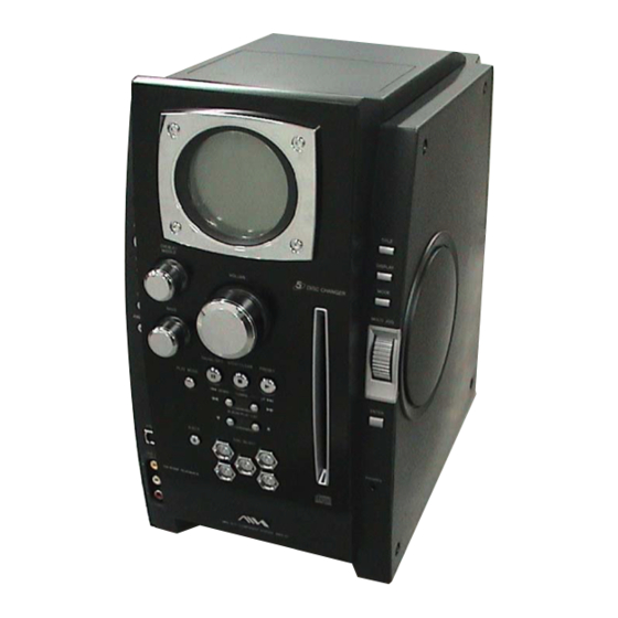
Page 6: General
CX-BK1 SECTION 2 This section is extracted from instruction manual. GENERAL • LOCATION OF CONTROLS Main unit: front 6 PLA Y MODE (US model) TITLE Selects various CD play mode. When the unit is turned off: activates or deactivated DEMO. - Page 7 CX-BK1 7 SHIFT Remote commander TUNER MODE Hold down when pressing a numbered button to change Switches between stereo or monaural FM reception. Refer to the pages indicated in parentheses for details. its function to that printed above the number.
-
Page 8: Disassembly
CX-BK1 SECTION 3 DISASSEMBLY • This set can be disassembled in the order shown below. 3-1. DISASSEMBLY FLOW Note 1: The process described in can be performed in any order. Note 2: Without completing the process described in , the next process can not be performed. -
Page 9: Panel
CX-BK1 Note: Follow the disassembly procedure in the numerical order given. 1 three screws 3-2. PANEL (BVTP3 × 10) • Tape deck is not loaded in US model. The shape of the top panel shown in “DISASSEMBLY” is different from the actual shape. -
Page 10: Front Panel Assy
CX-BK1 E51, MX 3-4. FRONT PANEL ASSY 3 wire (flat type) (5core) (CN504) 2 wire (flat type) (17core) (CN004) 1 wire (flat type) (19core) (CN905) 9 front panel assy 6 two screws 8 two claws (BVTP3 × 10) 4 connector (CN530) 5 five screws (BVTP3 ×... -
Page 11: Rear Cover
CX-BK1 3-6. REAR COVER 1 seven screws (BVTP3 × 10) 3 connector (CN303) 4 rear cover 3-7. TUNER (FM/AM) 1 two screws 2 tuner (FM/AM) (BVTP3 × 8) -
Page 12: Speaker Board
CX-BK1 3-8. SPEAKER BOARD 2 two screws (BVTP3 × 10) 3 speaker board 1 connector (CN503) 3-9. ACDC BOARD, POWER TRANSFORMER 4 two screws 1 connector (CN003) (BVTP3 × 10) 2 connector (CN006) 6 ACDC board 5 seven screws (BVTP3 × 10) -
Page 13: Amp Board
CX-BK1 3-10. AMP BOARD 4 two screws (BVTP3 × 10) 3 two screws (BVTP3 × 10) 5 AMP board 2 CD support board 1 two screws (BVTP3 × 10) 3-11. CD MECHANISM DECK (CDM69BV-30CBD64NS) 1 four screws (BVTP3 × 10) -
Page 14: Signal Cassette Mechanism
CX-BK1 3-12. SIGNAL CASSETTE MECHANISM • Tape deck is not loaded in US model. 1 connector (CN302) 3 signal cassette mechanism 2 four screws (BVTP3 × 10) 3-13. BASE UNIT SECTION 2 screw (+PTPWH) (M2) (DIA. 7) 3 boss 1 floating screw (DIA. 12) -
Page 15: Base Unit (Bu-30Cbd64Ns)
CX-BK1 3-14. BASE UNIT (BU-30CBD64NS) qa base unit (BU-30CBD64NS) 4 floating screw (+PTPWHM2.6 × 6) 1 tension spring (BU30-1) 9 vibration proof rubber 5 floating screw (+PTPWHM2.6 × 6) 3 floating screw (+PTPWHM2.6 × 6) q; vibration proof rubbers 8 vibration proof rubber 2 floating screw (+PTPWHM2.6 ×... -
Page 16: Sw (1) Board, Sw (2) Board, Sw (3) Board, Sw (4) Board, Bracket (Top) Assy
CX-BK1 3-16. SW (1) BOARD, SW (2) BOARD, SW (3) BOARD, SW (4) BOARD, BRACKET (TOP) ASSY 4 SW (3) board 5 SW (4) board 3 SW (2) board 1 four screws (BTP2.6 × 6) 6 six screws (BVTP2.6 × 8) -
Page 17: Motor (Stocker) Assy (Stocker) (M761)
CX-BK1 3-18. MOTOR (STOCKER) ASSY (STOCKER) (M761) 3 two screws (BVTP2.6 × 8) 2 Remove two solders 5 stocker motor board 6 motor (stocker) assy (stocker) (M761) 1 belt (stocker) 3-19. MOTOR (ROLLER) ASSY (ROLLER) (M781) 3 two screws 2 Remove two solders. -
Page 18: Motor (Mode) Assy (Mode) (M771)
CX-BK1 3-20. MOTOR (MODE) ASSY (MODE) (M771) 3 two screws (BVTP2.6 × 8) 1 Remove five solders of rotary encoder. 4 MODE MOTOR board 6 motor (mode) assy (mode) (M771) MODE MOTOR board 2 Remove two solders of motor (M771) 5 belt (mode V) 3-21. -
Page 19: Timing Belt (Front/Rear)
CX-BK1 3-22. TIMING BELT (FRONT/REAR) 3 slider (mode cam) assy 7 two gears (center) When install three timing belts, its pass under each claws. 8 timing belt (rear) timing belt (rear) 5 two gears 9 timing belt (rear) (center) claw... -
Page 20: Sensor Board
CX-BK1 3-24. SENSOR BOARD ql harness qk claw q; cam (eject lock) : Note 9 screw (PTPWH2.6 × 8) qh two claws qd gear (eject lock) qj rotary encoder 8 shaft qs cam (BU U/D) (S771) wa SENSOR board (shutter) w;... -
Page 21: Assembly
CX-BK1 SECTION 4 ASSEMBLY • This set can be assembled in the order shown below. 4-1. HOW TO INSTALL THE CAM (EJECT LOCK) 1 Rotate the cam (BU U/D) fully in the direction of arrow. 2 Engage the gear (eject lock) and the gear of the cam (eject lock) aligning the mark with the center of the gear (eject lock). -
Page 22: How To Install The Gear (Mode C)
CX-BK1 4-3. HOW TO INSTALL THE GEAR (MODE C) 1 Align the mark on the rotary encoder (S771) with the projection of the assy. 2 Check that the cam (BU U/D) can not be rotated in the direction of arrow. -
Page 23: How To Install The Rotary Encoder (S702), Gear (Stocker Communication)
CX-BK1 4-5. HOW TO INSTALL THE ROTARY ENCODER (S702), GEAR (STOCKER COMMUNICATION) 4 gear 5 screw (stocker communication) (PTPWH2.6 × 8) 3 screw 7 two screws (PWH2 × 6) (PTPWH2.6 × 8) 1 rotary encoder Engage the rotary encoder (S702) -
Page 24: Test Mode
CX-BK1 SECTION 5 TEST MODE [Cold Reset] sage “EQ MAX”, “EQ MIN” or “EQ FLAT” is displayed in The cold reset clears all data including preset data stored in this order. the RAM to initial conditions. Execute this mode when re- turning the set to the customer. -
Page 25: Mechanical Adjustments
CX-BK1 SECTION 6 SECTION 7 MECHANICAL ADJUSTMENTS ELECTRICAL ADJUSTMENTS • TAPE MECHANISM DECK SECTION DECK SECTION 0 dB = 0.775 V Note: Tape deck is not loaded in US model. Note: Tape deck is not loaded in US model. Precaution Precaution 1. - Page 26 CX-BK1 3. Mode: Playback Record Bias Adjustment Procedure: SPEAKER board Record mode SPEAKER terminal (JK502) test tape L-CH P-4-A100 oscilloscope (10 kHz, – 10 dB) MAIN board L-CH AUX IN jack (JK602) 1) 315 Hz 50 mV (–23.8 dB) ...
- Page 27 CX-BK1 – DECK Board (Component Side) (Except US model) – SFR452 SFR451 Record Bias Record Bias Adjustment Adjustment (R-CH) (L-CH) – MAIN Board (Conductor Side) – JK602 AUX IN jack (R-CH) AUX IN jack (R-CH) – SPEAKER Board (Conductor Side) –...
-
Page 28: Cd Section
CX-BK1 RFDC signal waveform CD SECTION VOLT/DIV: 200 mV TIME/DIV: 500 ns Note: 1. Use YEDS-18 disc (3-702-101-01) unless otherwise indicated. 2. Use an oscilloscope with more than 10MΩ impedance. 3. Clean the object lens by an applicator with neutral detergent when the level: 0.6 ±... - Page 29 CX-BK1 E-F Balance Adjustment Checking Location: Connection: – BD BOARD (Side B) – oscilloscope BD board TP (TE) TP (VC) – Procedure: Connect an oscilloscpe to test point TP (TE) and TP (VC) on the BD board. AC is put in pushing button to enter the CD test mode.
- Page 30 CX-BK1 MEMO...
-
Page 31: Diagrams
CX-BK1 SECTION 8 DIAGRAMS 8-1. BLOCK DIAGRAM – CD Section – • R-ch is omitted due to same as L-ch. • SIGNAL PATH : CD OPTICAL PICK-UP DIGITAL SERVO, RF AMP DIGITAL SIGNAL PROCESSOR : DIGITAL OUT BLOCK IC101 IC103... -
Page 32: Block Diagram - Tuner/Tape/Usb Section
CX-BK1 8-2. BLOCK DIAGRAM – TUNER/TAPE/USB Section – (Chilean, Peruvian, Mexican) MIC LEVEL • R-ch is omitted due to same as L-ch. Q201 • SIGNAL PATH VR201 J201 MIC MIXING : CD MIC AMP MIC AMP : TUNER IC201 (1/2) -
Page 33: Block Diagram - Amp Section
CX-BK1 8-3. BLOCK DIAGRAM – AMP Section – M301 (FAN) SWITCHING Q618 OUTPUT LEVEL • R-ch is omitted due to same as L-ch. DETECT R-CH R-CH Q620, 621 FAN MOTOR • SIGNAL PATH DRIVE : TUNER Q301 – 303 SWITCHING –... -
Page 34: Block Diagram - Power Supply Section
CX-BK1 8-4. BLOCK DIAGRAM – POWER SUPPLY Section – – VH POWER, VOLTAGE DC UNBALANCE POWER MONITOR POWER MONITOR AC DETECT (Page 33) DETECT DETECT Q105, 106 Q107 – 109 D139, 140 DC UNBALANCE RECT DETECT D116, 117 D112, 113... -
Page 35: Note For Printed Wiring Boards And Schematic Diagrams
CX-BK1 8-5. NOTE FOR PRINTED WIRING BOARDS AND SCHEMATIC DIAGRAMS • Circuit Boards Location Note on Printed Wiring Boards: Note on Schematic Diagram: tuner unit main board • X : parts extracted from the component side. • All capacitors are in µF unless otherwise noted. pF: µµF •... -
Page 36: Printed Wiring Board - Bd Board
CX-BK1 8-6. PRINTED WIRING BOARD – BD Board – • See page 35 for Circuit Boards Location. :Uses unleaded solder. • Semiconductor Location Ref. No. Location IC101 IC102 IC103 IC104 IC121 Q101 C272 IC104 IC101 TP2(TE) CN507 (Page 43) TP6(RFDC) -
Page 37: Schematic Diagram - Bd Board
CX-BK1 8-7. SCHEMATIC DIAGRAM – BD Board – • • See page 42 for Waveforms. See page 68 for IC Block Diagrams. C203 1000p R216 C269 47 4V FB102 C256 C257 0.33 C263 C259 C270 220p 47 4V C255 C249... -
Page 38: Printed Wiring Boards - Changer Section
CX-BK1 8-8. PRINTED WIRING BOARDS – CHANGER Section – • :Uses unleaded solder. See page 35 for Circuit Boards Location. SW (1) BOARD (Page 43) SW (2) BOARD IC701 IC751 IC721 IC711 SW (3) BOARD S718 (STOCKING) SW (4) BOARD... -
Page 39: Schematic Diagram - Changer Section
CX-BK1 8-9. SCHEMATIC DIAGRAM – CHANGER Section – • See page 68 for IC Block Diagram. CN751 CN702 R731 DIODE DIODE IC751 D SENSE D SENSE R733 CN701 R734 DISC INSERT D+3.3V DETECT SENSOR 3 . 2 IC751 R732 M+12V... -
Page 40: Printed Wiring Board
CX-BK1 8-10. PRINTED WIRING BOARD – DECK Board (Except US model) – • :Uses unleaded solder. See page 35 for Circuit Boards Location. • Semiconductor Location Ref. No. Location D401 IC301 DECK BOARD IC401 R323 Q305 L451 CN008 Q306 C452... -
Page 41: Schematic Diagram
CX-BK1 8-11. SCHEMATIC DIAGRAM – DECK Board (Except US model) – • See page 42 for Waveforms. R306 JR303 3.9k C309 R307 R321 C317 IC301(1/2) CN008 R376 R317 R315 NJM14558M 1.2k 390k PB-L R313 C313 R303 REC-L 0.0068 R309 PB-R... - Page 42 CX-BK1 • Waveforms – DECK Board – – MAIN Board – – USB AUX Board – – BD Board – 1 IC103 qg (RFAC) (CD play mode) qa Q453, 454 Base (REC mode) wa IC901 qg (X2) ea IC700 2 (XTO) (USB mode) 1.2 Vp-p...
-
Page 43: Printed Wiring Board - Main Board
CX-BK1 8-12. PRINTED WIRING BOARD – MAIN Board – • See page 35 for Circuit Boards Location. :Uses unleaded solder. • Semiconductor Location (Page 48) (Page 40) Ref. No. Location USB AUX DECK BOARD FM 75Ω BOARD CN008 (COAXIAL) FM/AM/TUNER PACK... -
Page 44: Schematic Diagram - Main Board (1/4)
CX-BK1 8-13. SCHEMATIC DIAGRAM – MAIN Board (1/4) – • • See page 42 for Waveforms. See page 68 for IC Block Diagram. (1/4) CN901 ELV_E3 R901 ELV_E2 R920 R902 ELV_E1 C949 R950 C948 R903 100p 100p ELV_E0 R904 SLD_E3... -
Page 45: Schematic Diagram - Main Board (2/4)
CX-BK1 8-14. SCHEMATIC DIAGRAM – MAIN Board (2/4) – (2/4) (AEP,UK) IC604 GP1FA313TZ DIGITAL OPTICAL C668 C669 OPTICAL TRANSCEIVER CD_D-OUT D-GND (Page 44) C664 (E51,MX) CN504 R671 R676 R515 2.2k MIC-A-GND R699 MIC-OUT 5.6k I-MIC R516 R513 I-MIC D501 UDZSTE173.9B... -
Page 46: Schematic Diagram - Main Board (3/4)
CX-BK1 8-15. SCHEMATIC DIAGRAM – MAIN Board (3/4) – • See page 68 for IC Block Diagrams. (Page 44) (Page 44) (Page 44) (3/4) (AEP,UK) CN508 I-MIC RDS DATA RDS INT (AEP,UK) FM SIGNAL OUT C876 C866 C872 C873 +3V(RDS) 0.0033... -
Page 47: Schematic Diagram - Main Board (4/4)
CX-BK1 8-16. SCHEMATIC DIAGRAM – MAIN Board (4/4) – • See page 68 for IC Block Diagram. (Page 45) (4/4) R681 220k R677 CN007 Q625 2SC3052F-T 1-LF VSTBY(+9V) FEED BACK R680 R679 C675 Q624 220k 100k 0.015 SWITCH M-GND 2SK2158... -
Page 48: Printed Wiring Board - Usb Aux Board
CX-BK1 8-17. PRINTED WIRING BOARD – USB AUX Board – • :Uses unleaded solder. See page 35 for Circuit Boards Location. USB AUX BOARD EP702 C725 (CHASSIS) EP702 C724 C760 R736 X700 C715 R712 JW703 C706 C756 C759 C755 R707... -
Page 49: Schematic Diagram - Usb Aux Board
CX-BK1 8-18. SCHEMATIC DIAGRAM – USB AUX Board – • See page 42 for Waveform. R700 C710 R701 C717 C719 Q702 C700 C701 DTA114EKA-T146 USB ON/OFF SWITCH +5V REGULATOR IC701 Q701 C708 NJM78M05S 2SB1132-T1 C712 0.47 01-R 0.47 R710 220k... -
Page 50: Printed Wiring Boars - Mic Board (Chilean, Peruvian And Mexican Models)
CX-BK1 8-19. PRINTED WIRING BOARD – MIC Board (Chilean, Peruvian and Mexican models) – • See page 35 for Circuit Boards Location. :Uses unleaded solder. MIC BOARD VR201 (Page 43) MIC MIXING MAIN BOARD CN504 C216 CN205 C212 C206 R232... -
Page 51: Schematic Diagram - Mic Board (Chilean, Peruvian And Mexican Models)
CX-BK1 8-20. SCHEMATIC DIAGRAM – MIC Board (Chilean, Peruvian and Mexican models) – CN205 R208 LCK(NC) I-MIC MIC-OUT R214 C212 MIC-A-GND 0.47 C209 (Page 45) C211 R213 820p R210 2.2k R204 C204 0.22 R202 4.7k J201 C208 IC201(2/2) C216 R205... -
Page 52: Schematic Diagram - Amp Board (1/2)
CX-BK1 8-21. SCHEMATIC DIAGRAM – AMP Board (1/2) – (1/2) EP502 R541 D503 2.2k R529 1SS184-TE85L R537 4.7k R037 C524 (CHASSIS) 1k 1/2W (E51,MX) 5.6k R543 2.2k 1k 1/4W (US,AEP,UK) Q531 2SD2439 (US) ∗ R507 D510 R539 2SD2562 (E51,MX) 1SS181-TE85L Q507,509 1.2k... -
Page 53: Schematic Diagram - Amp Board (2/2)
CX-BK1 8-22. SCHEMATIC DIAGRAM – AMP Board (2/2) – (Page 52) (2/2) R695 D629 R681 R686 C636 1SS355TE-17 Q618 3.3k 100p 1/2W 2SK3053 SWITCHING C637 D623 1SS355TE-17 R699 3.3k Q620,621 ∗ R697,698 D626 OUTPUT LEVEL FMB-G16L R676 1.5k (E51,MX) DETECT 2.7k... -
Page 54: Printed Wiring Board - Amp Board
CX-BK1 8-23. PRINTED WIRING BOARD – AMP Board – • :Uses unleaded solder. See page 35 for Circuit Boards Location. AMP BOARD C521 R559 C522 R560 Q527 R561 R591 R066 R090 R562 (AEP) D020 Q012 C514 R037 C513 JW527 C517... -
Page 55: Printed Wiring Board - Headphone Board
CX-BK1 8-24. PRINTED WIRING BOARD – HEADPHONE Board – • 8-25. SCHEMATIC DIAGRAM – HEADPHONE Board – See page 35 for Circuit Boards Location. :Uses unleaded solder. HEADPHONE BOARD JW524 R525 R523 CN530 J521 JW523 PHONES JR501 O-P0WER JW523 BOARD... -
Page 56: Printed Wiring Board - Speaker Board
CX-BK1 8-26. PRINTED WIRING BOARD – SPEAKER Board – • See page 35 for Circuit Boards Location. :Uses unleaded solder. SPEAKER BOARD R571 C525 – C527 JK502 L501 SPEAKER C533 C535 R570 – BOARD CN601 (Page 54) L502 C534 C524... -
Page 57: Schematic Diagram - Speaker Board
CX-BK1 8-27. SCHEMATIC DIAGRAM – SPEAKER Board – CN503 FR SP OUT(R) FR SP GND(R) FR SP OUT(L) FR SP GND(L) L502 (Page 53) R570 1.7µH R571 L501 1/2W 1.7µH 1/2W JK502 C533 0.0022 SPEAKER C532 0.0022 R573 R572 C525... -
Page 58: Printed Wiring Boards - Key Section
CX-BK1 8-28. PRINTED WIRING BOARDS – KEY Section – • See page 35 for Circuit Boards Location. :Uses unleaded solder. • Semiconductor Location Ref. No. Location KEY LED RMC BOARD LEFT BUTTON BOARD IC601 IC602 S311 − 320, S331 − 339... -
Page 59: Schematic Diagram - Key Section
CX-BK1 8-29. SCHEMATIC DIAGRAM – KEY Section – • See page 42 for Waveform. Q601-605 LED DRIVE LED601 SLR-325VC (DISC SLOT ILLUMINATION) ~~ ~ CN613 CN612 Q601 Q602 Q603 Q604 Q605 FMA9AT148 FMA9AT148 FMA9TA148 FMA9TA148 FMA9TA148 R616 R617 R622 R618... -
Page 60: Printed Wiring Boards - Lcd Section
CX-BK1 8-30. PRINTED WIRING BOARDS – LCD Section – • See page 35 for Circuit Boards Location. :Uses unleaded solder. • Semiconductor Location Ref. No. Location RIGHT BUTTON (2) BOARD RIGHT BUTTON (1) BOARD LCD VOL BOARD IC001 R252 JR108... -
Page 61: Schematic Diagram - Lcd Section
CX-BK1 8-31. SCHEMATIC DIAGRAM – LCD Section – R252 R251 R253 R254 R255 R256 R257 R258 LED254 LED252 LED206 LED209 LED212 LED215 LED218 LED221 LED,SELU1910CXM LED,SELU1910CXM SLR-325DCT31 SLR-325DCT31 SLR-325DCT31 SLR-325DCT31 SLR-325DCT31 SLR-325DCT31 LF38 LF38 LED253 LED251 LED205 LED208 LED211 LED214... -
Page 62: Printed Wiring Board - Acdc Board
CX-BK1 8-32. PRINTED WIRING BOARD – ACDC Board – • See page 35 for Circuit Boards Location. :Uses unleaded solder. • Semiconductor Location Ref. No. Location (E51) S001 (Page 54) D002 VOLTAGE SELECTOR 220V − 230V 120V 240V D004 AMP BOARD... -
Page 63: Schematic Diagram - Acdc Board
CX-BK1 8-33. SCHEMATIC DIAGRAM – ACDC Board – CN006 REG-GND(+7V) C008 REG-GND(+4V) JW091 100V REG-GND(+12V) JW090 (Page 53) D004 CN003 D5SBA20 (US,AEP,UK) D10XB20 (E51,MX) (AEP, UK) CN009 JW082 C016 ∗ C015,016 ∗ VH(AC) 3300 63V (AEP,UK) VH(AC) 3300 71V (US) -
Page 64: Printed Wiring Board - Pt Board (Us, Aep And Uk Models)
CX-BK1 8-34. PRINTED WIRING BOARD – PT Board (US, AEP and UK models) – • :Uses unleaded solder. See page 35 for Circuit Boards Location. ACDC BOARD (Page 62) PT BOARD CN010 ∗ NOT REPLACEABLE: BUILT IN TRANSFORMER PT003 POWER TRANSFOEMER... -
Page 65: Schematic Diagram - Pt Board (Us, Aep And Uk Models)
CX-BK1 8-35. SCHEMATIC DIAGRAM – PT Board (US, AEP and UK models) – (AEP, UK) CN011 PT003 POWER TRANSFORMER VH(AC) (MAIN) VH(AC) VL(AC) VL(AC) (Page 63) (US) ∗ CN001 VH(AC) VH(AC) VL(AC) CN010 VL(AC) REG (AC) REG (AC) (Page 63) -
Page 66: Printed Wiring Board - Pt Board (Chilean, Peruvian And Mexican Models)
CX-BK1 8-36. PRINTED WIRING BOARD – PT Board (Chilean, Peruvian and Mexican models) – • See page 35 for Circuit Boards Location. :Uses unleaded solder. PT001 (MX) (E51) ∗ (Page 62) (Page 62) ACDC BOARD ACDC BOARD PT BOARD ∗... -
Page 67: Schematic Diagram - Pt Board (Chilean, Peruvian And Mexican Models)
CX-BK1 8-37. SCHEMATIC DIAGRAM – PT Board (Chilean, Peruvian and Mexican models) – (E51) PT002 POWER TRANSFORMER (MAIN) ∗ ∗ NOT REPLACEABLE: BUILT IN TRANSFORMER (MX) PT001 POWER TRANSFORMER (MAIN) (E51) CN008 ∗ (Page 63) CN007 CN015 VH(AC) VH(AC) (Page 63) - Page 68 CX-BK1 • IC Block Diagrams – BD Board – IC101 CXD3068Q IC102 AN41020A 59 58 57 56 55 54 53 52 51 50 49 48 47 46 45 44 43 42 41 DVDD2 ASYE PVCC/2 DIGITAL ASYMMETRY CORRECTOR DIGITAL DOUT...
- Page 69 CX-BK1 IC103 CXA2647N-T4 ROM/RW DC OFST RFDCI – – RFDC – ROM/RW VOFST APC AMP RF OFF AT VCC RFAC EQ IN ROM/RW RFAC AC SUM SUMMING VOFST – – ROM/RW TE BAL ROM/RW – VOFST – – DVC OR Hi-Z...
- Page 70 CX-BK1 IC104 TC94A20F-CX4 Timing SubQ General Generator /RESET Input Port MIMD /MICS /MILP VSSM MIDIO /MICK /MIACK VDDM VDDT BCKO MP3REQ LRCKO SDIO BCKIA LRCKIA VDDT Switch SDI1 BCKIB...
- Page 71 CX-BK1 – CONNECTOR Board – – MAIN Board – IC701, 711, 721 BA6956AN IC501 BU4052BCF-E2 2XCOM CONTROL LOGIC XCOM IC601 M61529FP-D60G 42 41 39 38 37 34 33 32 31 30 TONE CONTROL ELECTRICAL (BASS/MID/TREBLE) VOLUME INPUT BASS BOOST TONE ATT...
- Page 72 CX-BK1 IC603 NJM2156M (TE2) 19 18 17 16 12 11 BIAS MACH3 IC905 MM1614A CURRENT BIAS LIMITTER REFERENCE – DRIVER THERMAL SHUTDOWN...
-
Page 73: Ic Pin Function Description
CX-BK1 8-38. IC PIN FUNCTION DESCRIPTION • BD BOARD IC101 CXD3068Q (DIGITAL SERVO, DIGITAL SERVO PROCESSOR) Pin No. Pin Name Description DVDD0 — Power supply terminal (+3.3V) (digital system) XRST Reset signal input from the system controller “L”: reset MUTE Muting on/off control signal input terminal “H”: muting on Not used... - Page 74 CX-BK1 Pin No. Pin Name Description IGEN Stabilized current input for operational amplifiers AVDD0 — Power supply terminal (+3.3V) (analog system) ASYO EFM full-swing output terminal ASYI Asymmetry comparator voltage input terminal RFAC EFM signal input from the RF amplifier AVSS1 —...
- Page 75 CX-BK1 • MAIN BOARD IC901 uPD703260YGF-S04-JBT-A (SYSTEM CONTROLLER) Pin No. Pin Name Description RDS_SIG Tuning signal level input from the RDS decoder Used for the AEP, UK models RDS_DATA Serial data input from the RDS decoder Used for the AEP, UK models AVREF0 —...
- Page 76 CX-BK1 Pin No. Pin Name Description SHIFT_DATA Serial data output to the shift register SHIFT_STB Strobe signal output to the shift register PLLCE Latch signal output to the tuner unit PWM1 PWM signal output for focus offset adjustment MCLK Serial data transfer clock signal output to the tuner unit and input select IC...
- Page 77 CX-BK1 Pin No. Pin Name Description ELV_E0 ELV_E0 switch signal input from the CD mechanism RE_TRE Jog dial pulse input from the rotary encoder (TREBLE/MIDDLE) RE_BAS Jog dial pulse input from the rotary encoder (BASS) RE_VOL Jog dial pulse input from the rotary encoder (VOLUME)
- Page 78 CX-BK1 • USB AUX BOARD IC700 uAC3553B (USB INTERFACE) Pin No. Pin Name Description System clock input terminal (12MHz) System clock output terminal (12MHz) AREG1 Connected to the external capacitor AVSS_12 — Ground terminal OUTL USB audio signal output terminal (L-ch)
-
Page 79: Exploded Views
CX-BK1 SECTION 9 EXPLODED VIEWS NOTE: • -XX and -X mean standardized parts, so they • Items marked “*” are not stocked since they The components identified by mark 0 or dotted line with mark may have some difference from the original are seldom required for routine service. -
Page 80: Top Panel Block
CX-BK1 9-2. TOP PANEL BLOCK Note: Tape deck is not loaded in US model. The shape of the top panel shown in “EXPLODED VIEWS” is different from the actual shape. supplied not supplied not supplied Ref. No. Part No. Description Remark Ref. -
Page 81: Front Panel Block-1
CX-BK1 9-3. FRONT PANEL BLOCK-1 not supplied not supplied (LED board) front panel block-2 Ref. No. Part No. Description Remark Ref. No. Part No. Description Remark A-4733-419-A MIC BOARD, COMPLETE (E51, MX) A-4733-395-A KEY LED RMC BOARD, COMPLETE 1-769-869-11 WIRE (FLAT TYPE) (5 CORE) (E51, MX) -
Page 82: Front Panel Block-2
CX-BK1 9-4. FRONT PANEL BLOCK-2 not supplied front panel block-3 Ref. No. Part No. Description Remark Ref. No. Part No. Description Remark X-4955-595-1 VOL ASSY, KNOB RTRY 4-245-101-01 KNOB (JOG), ROTARY X-4955-596-1 TRE ASSY, KNOB RTRY 1-688-408-11 RIGHT BUTTON (1) BOARD... -
Page 83: Front Panel Block-3
CX-BK1 9-5. FRONT PANEL BLOCK-3 not supplied not supplied Ref. No. Part No. Description Remark Ref. No. Part No. Description Remark X-4955-409-2 CABI, FR ASSY (US) 4-245-088-01 WINDOW, SENSOR X-4955-727-2 CABINET (FRONT) ASSY (E51, MX) 4-245-094-01 PANEL, CD DIRECT X-4955-728-2 CABINET (FRONT) ASSY (AEP, UK) -
Page 84: Chassis Block-1
CX-BK1 9-6. CHASSIS BLOCK-1 not supplied chassis block-2 PT001 (MX) PT002 (E51) not supplied PT003 (US, AEP, UK) The components identified by mark 0 or dotted line with mark 0 are critical for safety. Replace only with part number specified. -
Page 85: Chassis Block-2
CX-BK1 9-7. CHASSIS BLOCK-2 not supplied not supplied Q534 Q532 Q533 F001 Q531 not supplied CD mechanism deck section-1 not supplied not supplied (CD support board) not supplied not supplied not supplied The components identified by mark 0 or dotted line with mark 0 are critical for safety. -
Page 86: Cd Mechanism Deck Section-1 (Cdm69Bv-30Cbd64Ns)
CX-BK1 Ver 1.1 9-8. CD MECHANISM DECK SECTION-1 (CDM69BV-30CBD64NS) S702 M761 not supplied (ST encorder board) CD mechanism deck section-2 Ref. No. Part No. Description Remark Ref. No. Part No. Description Remark 1-686-725-12 STOCKER MOTOR BOARD 4-239-689-01 GEAR (STOCKER DECELERATION) 4-951-620-01 SCREW (2.6X8), +BVTP... -
Page 87: Cd Mechanism Deck Section-2 (Cdm69Bv-30Cbd64Ns)
CX-BK1 9-9. CD MECHANISM DECK SECTION-2 (CDM69BV-30CBD64NS) CD mechanism deck section-3 CD mechanism deck section-5 optical pick-up section Ref. No. Part No. Description Remark Ref. No. Part No. Description Remark 1-686-727-12 SW (1) BOARD 4-227-899-01 SCREW (DIA,12), FLOATING 1-686-728-12 SW (2) BOARD... -
Page 88: Cd Mechanism Deck Section-3 (Cdm69Bv-30Cbd64Ns)
CX-BK1 9-10. CD MECHANISM DECK SECTION-3 (CDM69BV-30CBD64NS) not supplied supplied not supplied supplied supplied not supplied Ref. No. Part No. Description Remark Ref. No. Part No. Description Remark X-4955-447-1 PULLEY (A)(BU30) ASSY,CHUCKING 4-243-291-01 SPRING, TORSION 4-992-069-01 SCREW (+PTPWH) (M2) (DIA. 7) -
Page 89: Cd Mechanism Deck Section-4 (Cdm69Bv-30Cbd64Ns)
CX-BK1 9-11. CD MECHANISM DECK SECTION-4 (CDM69BV-30CBD64NS) supplied M781 CD mechanism deck section-5 Ref. No. Part No. Description Remark Ref. No. Part No. Description Remark X-4954-626-1 LEVER (ROLLER) ASSY 4-240-041-01 SPRING (SLIDER 2), TENSION 4-239-666-01 GEAR 4-951-620-01 SCREW (2.6X8), +BVTP... -
Page 90: Cd Mechanism Deck Section-5 (Cdm69Bv-30Cbd64Ns)
CX-BK1 9-12. CD MECHANISM DECK SECTION-5 (CDM69BV-30CBD64NS) CD mechanism deck section-6 Ref. No. Part No. Description Remark Ref. No. Part No. Description Remark 4-240-020-01 GEAR (TIMING) 4-239-699-01 PULLEY 4-239-708-02 BELT (FRONT), TIMING 4-247-349-02 BELT (ROLLER V) 4-239-697-01 GEAR (CENTER) 4-227-899-01 SCREW (DIA. 12), FLOATING... -
Page 91: Cd Mechanism Deck Section-6 (Cdm69Bv-30Cbd64Ns)
CX-BK1 9-13. CD MECHANISM DECK SECTION-6 (CDM69BV-30CBD64NS) not supplied M771 supplied S771 Ref. No. Part No. Description Remark Ref. No. Part No. Description Remark 4-239-693-02 CAM (GEAR) 4-239-692-02 CAM (BU U/D) 1-686-723-12 SENSOR BOARD 4-239-694-01 GEAR (MODE CAM) 4-239-696-01 GEAR (EJECT LOCK) -
Page 92: Optical Pick-Up Section (Bu-30Cbd64Ns)
CX-BK1 9-14. OPTICAL PICK-UP SECTION (BU-30CBD64NS) The components identified by mark 0 or dotted line with mark 0 are critical for safety. Replace only with part number specified. Ref. No. Part No. Description Remark Ref. No. Part No. Description Remark... -
Page 93: Electrical Parts List
CX-BK1 SECTION 10 ELECTRICAL PARTS LIST ACDC NOTE: • Due to standardization, replacements in the • Items marked “*” are not stocked since they The components identified by mark 0 or dotted line with mark parts list may be different from the parts speci- are seldom required for routine service. - Page 94 CX-BK1 ACDC Ref. No. Part No. Description Remark Ref. No. Part No. Description Remark Q102 8-729-120-28 TRANSISTOR 2SC3052F-T1-LF R157 1-216-827-11 METAL CHIP 3.3K 1/10W Q103 8-729-120-28 TRANSISTOR 2SC3052F-T1-LF (US) Q104 6-550-580-01 TRANSISTOR 2SA1235TP-1F R157 1-216-828-11 METAL CHIP 3.9K 1/10W Q105...
- Page 95 CX-BK1 Ref. No. Part No. Description Remark Ref. No. Part No. Description Remark C633 1-126-947-11 ELECT 47uF < SHORT > C634 1-128-552-51 ELECT 47uF JR511 1-216-296-00 SHORT CHIP C635 1-163-833-00 CERAMIC CHIP 0.068uF JR512 1-216-296-00 SHORT CHIP C636 1-162-927-11 CERAMIC CHIP...
- Page 96 CX-BK1 Ref. No. Part No. Description Remark Ref. No. Part No. Description Remark R065 1-216-073-00 RES-CHIP 1/10W R536 1-216-809-11 METAL CHIP 1/10W R066 1-216-085-00 RES-CHIP 1/10W R537 1-247-713-11 CARBON 1/2W R067 1-216-089-11 RES-CHIP 1/10W (E51, MX) R068 1-216-833-11 METAL CHIP...
- Page 97 CX-BK1 Ref. No. Part No. Description Remark Ref. No. Part No. Description Remark 0 R598 1-220-755-11 METAL 0.22 R698 1-216-053-00 METAL CHIP 1.5K 1/10W (AEP, UK) (E51, MX) 0 R598 1-217-153-00 METAL 0.47 R698 1-216-055-00 METAL CHIP 1.8K 1/10W (E51, MX)
- Page 98 CX-BK1 Ref. No. Part No. Description Remark Ref. No. Part No. Description Remark < SHORT > C226 1-126-607-11 ELECT CHIP 47uF C227 1-164-360-11 CERAMIC CHIP 0.1uF 1-216-864-11 SHORT CHIP C229 1-164-360-11 CERAMIC CHIP 0.1uF C230 1-164-360-11 CERAMIC CHIP 0.1uF < COIL >...
- Page 99 CX-BK1 CONNECTOR DECK Ref. No. Part No. Description Remark Ref. No. Part No. Description Remark R225 1-216-809-11 METAL CHIP 1/10W C761 1-162-306-11 CERAMIC 0.01uF R226 1-216-809-11 METAL CHIP 1/10W C762 1-164-159-21 CERAMIC 0.1uF R227 1-216-809-11 METAL CHIP 1/10W R230 1-216-811-11 METAL CHIP...
- Page 100 CX-BK1 DECK Ref. No. Part No. Description Remark Ref. No. Part No. Description Remark C318 1-126-956-91 ELECT 0.1uF JR401 1-216-295-00 SHORT CHIP C325 1-164-156-11 CERAMIC CHIP 0.1uF JR402 1-216-296-00 SHORT CHIP C326 1-164-227-11 CERAMIC CHIP 0.022uF C327 1-107-826-11 CERAMIC CHIP 0.1uF...
- Page 101 CX-BK1 DECK HEADPHONE KEY LED RMC Ref. No. Part No. Description Remark Ref. No. Part No. Description Remark R417 1-216-833-11 METAL CHIP 1/10W < RESISTOR > R418 1-216-833-11 METAL CHIP 1/10W R419 1-216-821-11 METAL CHIP 1/10W R376 1-216-833-11 METAL CHIP...
- Page 102 CX-BK1 KEY LED RMC LCD VOL Ref. No. Part No. Description Remark Ref. No. Part No. Description Remark Q604 6-550-336-01 TRANSISTOR FMA9AT148 S334 1-771-410-21 SWITCH, TACTILE (TUNING DOWN . m) Q605 6-550-336-01 TRANSISTOR FMA9AT148 ************************************************************** < RESISTOR > A-4733-394-A LCD VOL BOARD, COMPLETE...
- Page 103 CX-BK1 LCD VOL LEFT BUTTON MAIN Ref. No. Part No. Description Remark Ref. No. Part No. Description Remark LED BOARD LED209 8-719-061-96 LED SLR-325DCT31 (ILLUMINATION) ********** LED210 8-719-061-96 LED SLR-325DCT31 (ILLUMINATION) LED211 8-719-061-96 LED SLR-325DCT31 (ILLUMINATION) < LED > LED212 8-719-061-96 LED SLR-325DCT31 (ILLUMINATION)
- Page 104 CX-BK1 MAIN Ref. No. Part No. Description Remark Ref. No. Part No. Description Remark C518 1-104-665-11 ELECT 100uF C676 1-126-960-11 ELECT C519 1-104-665-11 ELECT 100uF C601 1-124-261-00 ELECT 10uF C677 1-107-826-11 CERAMIC CHIP 0.1uF C602 1-124-261-00 ELECT 10uF C682 1-137-367-11 MYLAR 0.0033uF 5%...
- Page 105 CX-BK1 MAIN Ref. No. Part No. Description Remark Ref. No. Part No. Description Remark C934 1-126-933-11 ELECT 100uF D910 8-719-423-10 DIODE MA8100-M-TX C935 1-164-227-11 CERAMIC CHIP 0.022uF C936 1-126-933-11 ELECT 100uF D911 8-719-988-61 DIODE 1SS355TE-17 C938 1-126-960-11 ELECT C939 1-164-156-11 CERAMIC CHIP 0.1uF...
- Page 106 CX-BK1 MAIN Ref. No. Part No. Description Remark Ref. No. Part No. Description Remark JR907 1-216-864-11 SHORT CHIP R515 1-216-837-11 METAL CHIP 1/10W JR908 1-216-864-11 SHORT CHIP 0 (AEP, UK) R516 1-216-837-11 METAL CHIP 1/10W < SHORT > R517 1-216-174-11 METAL CHIP...
- Page 107 CX-BK1 MAIN Ref. No. Part No. Description Remark Ref. No. Part No. Description Remark R651 1-216-845-11 METAL CHIP 100K 1/10W R718 1-216-833-11 METAL CHIP 1/10W R652 1-216-845-11 METAL CHIP 100K 1/10W R719 1-216-833-11 METAL CHIP 1/10W R655 1-216-824-11 METAL CHIP 4.7K...
- Page 108 CX-BK1 MAIN Ref. No. Part No. Description Remark Ref. No. Part No. Description Remark R937 1-216-809-11 METAL CHIP 1/10W R785 1-216-841-11 METAL CHIP 1/10W R938 1-216-809-11 METAL CHIP 1/10W R786 1-216-841-11 METAL CHIP 1/10W R939 1-216-809-11 METAL CHIP 1/10W R787...
- Page 109 CX-BK1 MAIN MODE MOTOR RIGHT BUTTON (1) Ref. No. Part No. Description Remark Ref. No. Part No. Description Remark R996 1-216-864-11 SHORT CHIP 0 (AEP, UK) R204 1-216-809-11 METAL CHIP 1/10W R997 1-216-833-11 METAL CHIP 1/10W R205 1-216-825-11 METAL CHIP 2.2K...
- Page 110 CX-BK1 RIGHT BUTTON (2) ROLLER MOTOR SENSOR SPEAKER STOCKER SW (1) SW (2) SW (3) SW (4) USB AUX Ref. No. Part No. Description Remark Ref. No. Part No. Description Remark 1-686-727-12 SW (1) BOARD 1-688-409-11 RIGHT BUTTON (2) BOARD...
- Page 111 CX-BK1 USB AUX Ref. No. Part No. Description Remark Ref. No. Part No. Description Remark C755 1-162-927-11 CERAMIC CHIP 100PF R716 1-216-827-11 METAL CHIP 3.3K 1/10W R718 1-216-827-11 METAL CHIP 3.3K 1/10W C756 1-126-963-11 ELECT 4.7uF R720 1-216-827-11 METAL CHIP 3.3K...
- Page 112 CX-BK1 Ref. No. Part No. Description Remark Ref. No. Part No. Description Remark Q531 6-550-320-01 TRANSISTOR 2SD2562 (E51, MX) Q531 8-729-020-52 TRANSISTOR 2SD2439-OPY (US) Q532 6-550-291-01 TRANSISTOR FN1016 (AEP, UK) Q532 6-550-320-01 TRANSISTOR 2SD2562 (E51, MX) Q532 8-729-020-52 TRANSISTOR 2SD2439-OPY (US)
- Page 113 CX-BK1 MEMO...
-
Page 114: Revision History
CX-BK1 REVISION HISTORY Clicking the version allows you to jump to the revised page. Also, clicking the version at the upper right on the revised page allows you to jump to the next revised page. Ver. Date Description of Revision 2003.06...