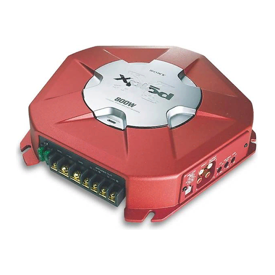
Sony XM-D400P5 Service Manual
Monaural power amplifier
Hide thumbs
Also See for XM-D400P5:
- Operating instructions (2 pages) ,
- Specifications (2 pages) ,
- Limited warranty (1 page)
Table of Contents
Advertisement
QQ
3 7 63 1515 0
SERVICE MANUAL
Ver 1.0 2003. 01
AUDIO POWER SPECIFICATIONS (US MODEL)
POWER OUTPUT AND TOTAL HARMONIC DISTORTION
200 watts minimum continuous average power into 4 ohms,
20 Hz to 300 Hz with no more than 0.2% total harmonic
distortion per Car Audio Ad Hoc Committee standards.
TE
L 13942296513
Other Specifications
Circuit system
Class D Technology
Pulse power supply
Inputs
RCA pin jacks
High level input connector
Outputs
Speaker terminals
Through out pin jacks
Suitable speaker impedance
2 – 8 Ω
Maximum outputs
400 W (at 4 Ω)
800 W (at 2 Ω)
Rated outputs (supply voltage at 14.4 V)
200 W (20 Hz – 300 Hz, 0.2% THD, at 4 Ω)
400 W (20 Hz – 300 Hz, 0.6% THD, at 2 Ω)
Frequency response
5 Hz – 300 Hz (
Harmonic distortion
0.06% or less (at 100 Hz, 4 Ω)
Input level adjustment range
0.3 – 6.0 V (RCA pin jacks)
1.2 – 12.0 V (High level input)
www
.
Sony Corporation
9-877-038-01
2003A0400-1
e Vehicle Company
© 2003. 01
Published by Sony Engineering Corporation
http://www.xiaoyu163.com
+0.5
dB)
–3
x
ao
u163
y
i
http://www.xiaoyu163.com
XM-D400P5
2 9
8
SPECIFICATIONS
Q Q
3
6 7
1 3
1 5
Low-pass filter
Low boost
Power requirements
Power supply voltage
Current drain
Dimensions
Mass
Supplied accessories
Design and specifications are subject to change without
notice.
Notes on Chip Component Replacement
• Never reuse a disconnected chip component.
• Notice that the minus side of a tantalum capacitor may be
damaged by heat.
MONAURAL POWER AMPLIFIER
co
.
9 4
2 8
US Model
Canadian Model
AEP Model
UK Model
E Model
0 5
8
2 9
9 4
2 8
50 – 300 Hz, –12 dB/oct
0 – 10 dB (40 Hz)
12 V DC car battery
(negative ground)
10.5 – 16 V
at rated output : 62 A (at 2 Ω)
Remote input : 2 mA
Approx. 295 × 57 × 290 mm
(11
× 2
× 11
in.) (w/h/d) not incl.
5/8
1/4
1/2
projecting parts and controls
Approx. 2.8 kg (6 lb. 3 oz.) not incl. accessories
Mounting screws (5)
High level input cord (1)
Protection cap (1)
m
9 9
9 9
1
Advertisement
Table of Contents

Related Manuals for Sony XM-D400P5


Summary of Contents for Sony XM-D400P5
- Page 1 • Never reuse a disconnected chip component. • Notice that the minus side of a tantalum capacitor may be damaged by heat. MONAURAL POWER AMPLIFIER u163 Sony Corporation 9-877-038-01 2003A0400-1 e Vehicle Company © 2003. 01 Published by Sony Engineering Corporation http://www.xiaoyu163.com...
-
Page 2: Table Of Contents
XM-D400P5 3 7 63 1515 0 TABLE OF CONTENTS 1. GENERAL Location and Function of Controls .......... 3 Connections ................4 2. DISASSEMBLY 2-1. Bottom Plate ................ 6 2-2. Main Board Section ............. 7 2-3. Disassembly and Assembly of Ornamental Plate ....7 2-4. -
Page 3: General
XM-D400P5 SECTION 1 GENERAL 3 7 63 1515 0 This section is extracted from instruction manual. Location and Function of Controls Emplacement et fonction des commandes 1 POWER/PROTECTOR indicator 1 Indicateur POWER/PROTECTOR POWER/PROTECTOR Lights up in green during operation. -
Page 4: Connections
• Do not connect any active speakers (with built-in the ground terminal of the car battery to avoid la borne de masse de la batterie de voiture In such a case, consult your nearest Sony dealer. amplifiers) to the speaker terminals of the unit. short circuits. - Page 5 XM-D400P5 3 7 63 1515 0 Input Connections Connexions d’entrée For details on the settings of switches and controls, refer to “Location and Function of Controls.” Pour plus de détails sur les réglages des commutateurs et commandes, reportez-vous à “Emplacement et fonction des commandes”.
-
Page 6: Disassembly
XM-D400P5 SECTION 2 DISASSEMBLY 3 7 63 1515 0 Note : This set can be disassemble according to the following sequence. 2-1. BOTTOM PLATE (Page 6) 2-2. MAIN BOARD SECTION (Page 7) 2-5. LED BOARD 2-3. DISASSMBLY AND ASSEMBLY 2-4. -
Page 7: Main Board Section
XM-D400P5 3 7 63 1515 0 2-2. MAIN BOARD SECTION 2 P 3x6 3 BTP 3x14 4 BTP 3x14 6 MAIN board section 5 BTP 3x14 1 P 3x8 heat sink (main) 7 CNT2 L 13942296513 2-3. DISASSEMBLY AND ASSEMBLY OF ORNAMENTAL PLATE... -
Page 8: Main Board
XM-D400P5 3 7 63 1515 0 2-4. MAIN BOARD 2 P 3x8 1 P 3x8 4 MAIN board 3 panel (front) L 13942296513 2-5. LED BOARD 1 P 3x6 2 LED board heat sink (main) u163 http://www.xiaoyu163.com... -
Page 9: Diagrams
XM-D400P5 SECTION 3 DIAGRAMS 3 7 6 3 1 5 1 5 0 3-1. IC BLOCK DIAGRAM THIS NOTE IS COMMON FOR PRINTED WIRING BOARDS AND SCHEMATIC DIAGRAMS. (In addition to this, the necessary note is IC6 TL494CN printed in each block.) -
Page 10: Printed Wiring Boards -Main Section (1/2)
XM-D400P5 3 7 6 3 1 5 1 5 0 3-2. PRINTED WIRING BOARDS — MAIN SECTION (1/2) — • Refer to page 9 for Common Note on Printed Wiring Boards. MAIN BOARD (SIDE A) • Semiconductor Location (Side A) Ref. -
Page 11: Printed Wiring Boards -Main Section (2/2)
XM-D400P5 3 7 6 3 1 5 1 5 0 3-3. PRINTED WIRING BOARDS — MAIN SECTION (2/2) — • Refer to page 9 for Common Note on Printed Wiring Boards. MAIN BOARD (SIDE B) • Semiconductor MC14 Location (Side B) Ref. -
Page 12: Schematic Diagram -Main Section (1/2)
XM-D400P5 3 7 6 3 1 5 1 5 0 3-4. SCHEMATIC DIAGRAM — MAIN SECTION (1/2) — • Refer to page 9 for Common Note on Schematic Diagram. R136 CNT1 IC1(1/2) IC2(1/2) IC3(1/2) R163 IC4(2/2) IC5(2/2) EC51 R164... -
Page 13: Schematic Diagram -Main Section (2/2)
XM-D400P5 3 7 6 3 1 5 1 5 0 3-5. SCHEMATIC DIAGRAM — MAIN SECTION (2/2) — • Refer to page 9 for Common Note on Schematic Diagram and IC Block Diagram. EC61 R112 R114 R115 R143 R110... - Page 14 XM-D400P5 3 7 6 3 1 5 1 5 0 MEMO 1 3 9 4 2 2 9 6 5 1 3 w w w u 1 6 3 http://www.xiaoyu163.com...
-
Page 15: Exploded Views
XM-D400P5 SECTION 4 EXPLODED VIEWS 3 7 63 1515 0 NOTE: • The mechanical parts with no reference • Color Indication of Appearance Parts The components identified by mark 0 or dotted line with mark number in the exploded views are not supplied. -
Page 16: Main Board Section
XM-D400P5 3 7 63 1515 0 4-2. MAIN BOARD SECTION not supplied not supplied not supplied L 13942296513 Ref. No. Part No. Description Remark Ref. No. Part No. Description Remark 3-253-080-01 PANEL (FRONT) 3-912-431-01 SCREW (+–P) A-3274-811-A MAIN BOARD, COMPLETE 3-912-432-01 SCREW (+–B) -
Page 17: Electrical Parts List
XM-D400P5 SECTION 5 MAIN ELECTRICAL PARTS LIST 3 7 63 1515 0 NOTE: • Due to standardization, replacements in • Items marked “*” are not stocked since The components identified by mark 0 or dotted line with mark the parts list may be different from the they are seldom required for routine service. - Page 18 XM-D400P5 MAIN 3 7 63 1515 0 Ref. No. Part No. Description Remark Ref. No. Part No. Description Remark 8-719-800-76 DIODE 1SS226 FET2 8-729-056-77 FET RFP70N06 8-719-987-67 DIODE 11EFS2 FET3 8-729-056-77 FET RFP70N06 8-719-987-67 DIODE 11EFS2 FET4 8-729-056-77 FET RFP70N06...
- Page 19 XM-D400P5 MAIN 3 7 63 1515 0 Ref. No. Part No. Description Remark Ref. No. Part No. Description Remark < TRANSFORMER > 1-216-073-00 METAL CHIP 1/10W 1-216-049-11 METAL CHIP 1/10W 1-439-760-11 TRANSFORMER, DC-DC CONVERTER 1-216-097-00 METAL CHIP 100K 1/10W...
- Page 20 XM-D400P5 MAIN 3 7 63 1515 0 Ref. No. Part No. Description Remark Ref. No. Part No. Description Remark 1-208-813-11 RES-CHIP 1/10W R150 1-216-198-00 METAL CHIP 1/8W 1-216-073-00 METAL CHIP 1/10W R151 1-216-198-00 METAL CHIP 1/8W 1-208-553-11 RES-CHIP 620K...
- Page 21 XM-D400P5 MAIN 3 7 63 1515 0 Ref. No. Part No. Description Remark < DIODE > 8-719-069-69 DIODE RD18F-T7B 8-719-069-69 DIODE RD18F-T7B 8-719-069-69 DIODE RD18F-T7B 8-719-069-69 DIODE RD18F-T7B 8-719-069-69 DIODE RD18F-T7B ************************************************************* MISCELLANEOUS *************** 0 FUSE1 1-532-947-11 FUSE (BLADE TYPE) (AUTO FUSE) (30A)
- Page 22 XM-D400P5 3 7 63 1515 0 REVISION HISTORY Clicking the version allows you to jump to the revised page. Also, clicking the version at the upper on the revised page allows you to jump to the next revised page.