
Related Manuals for Nokia NSB-6 Series


Summary of Contents for Nokia NSB-6 Series
- Page 1 PAMS Technical Documentation NSB–6 Series Transceivers System Module E Nokia Mobile Phones Ltd. Issue 1 06/2000...
-
Page 2: Table Of Contents
........E Nokia Mobile Phones Ltd. - Page 3 ......Parts list of UP9 (EDMS Issue 9.2) Code: 0201362 ..E Nokia Mobile Phones Ltd. Page 3 Issue 1 06/2000...
- Page 4 ..A–12 RF Testpoints of UP9 – Layout (Version 12) ....A–13 E Nokia Mobile Phones Ltd. Page 4 Issue 1 06/2000...
- Page 5 NSB–6 PAMS Technical Documentation System Module This page intentionally left blank. E Nokia Mobile Phones Ltd. Page 5 Issue 1 06/2000...
-
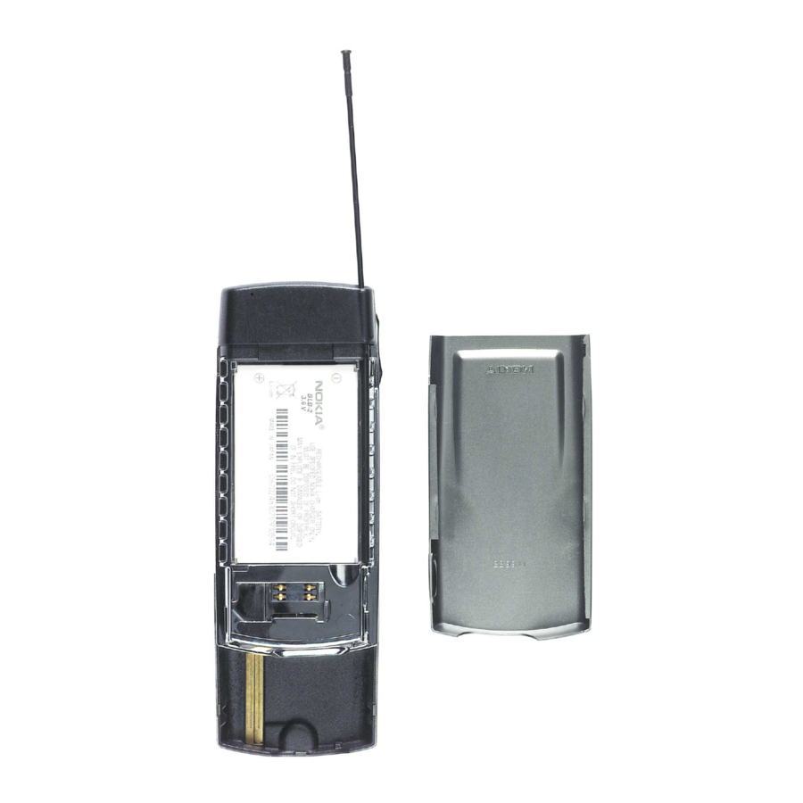
Page 6: Transceiver Nsb-6
The charge mode is effective in parallel with all previous modes. The charge mode itself consists of two different states, i.e. the fast charge and the maintenance mode. The local mode is used for alignment and testing. E Nokia Mobile Phones Ltd. Page 6 Issue 1 06/2000... -
Page 7: Interconnection Diagram
NSB–6 PAMS Technical Documentation System Module Interconnection Diagram Keyboard module module Battery Radio Module Charger Antenna Slide (mic.) IR Link Earpiece HF/HS E Nokia Mobile Phones Ltd. Page 7 Issue 1 06/2000... -
Page 8: System Module
Block Diagram TX/RX SIGNALS RF SUPPLIES PA SUPPLY 13MHz SYSTEM CLOCK COBBA SUPPLY COBBA CCONT 32kHz BB SUPPLY SLEEP CLOCK VBAT MEMORIES BATTERY CHAPS EXT. AUDIO BASEBAND Charger HS–connector connector E Nokia Mobile Phones Ltd. Page 8 Issue 1 06/2000... -
Page 9: Technical Summary
EMC shielding is implemented using a metallized plastic frame. On the other side the engine is shielded with PCB grounding. Heat generated by the circuitry will be conducted out via the PCB ground planes. E Nokia Mobile Phones Ltd. Page 9 Issue 1 06/2000... -
Page 10: External And Internal Signals And Connections
Battery voltage 2.85 Battery size indication Phone has 100kohm pull up resistor. SIM Card removal detection (Treshold is 2.4V@VBB=2.8V) kohm Battery indication resistor (BLB–2) kohm Battery indication resistor (service battery) E Nokia Mobile Phones Ltd. Page 10 Issue 1 06/2000... -
Page 11: Sim Card Connector
Notes Backup battery charg- 3.02 3.15 3.28 VBACK ing from CHAPS Backup battery charg- Vout@VBAT–0.2V ing from CHAPS Backup battery supply 3.28 VBACK to CCONT Backup battery supply to CCONT E Nokia Mobile Phones Ltd. Page 11 Issue 1 06/2000... -
Page 12: Power Distribution
At phone end there is no difference between a plug–in charger or a desktop charger. The DC–jack pins and bottom connector charging pads are connected together inside the phone. E Nokia Mobile Phones Ltd. Page 12 Issue 1 06/2000... -
Page 13: Startup Charging
The power switch is immediately turned OFF if the voltage in VOUT rises above the selected limit VLIM1 or VLIM2. Parameter Symbol LIM input Unit Output voltage cutoff limit VLIM (during transmission or Li– battery) E Nokia Mobile Phones Ltd. Page 13 Issue 1 06/2000... - Page 14 OFF until the the battery voltage falls below VLIM and PWM = LOW is detected. The switch can be turned on again by setting PWM = HIGH. VCH<VOUT VOUT VLIM SWITCH PWM (32Hz) E Nokia Mobile Phones Ltd. Page 14 Issue 1 06/2000...
-
Page 15: Battery Removal During Charging
4. Software sets PWM = LOW –> CHAPS does not enter PWM mode 5. PWM low –> Startup mode, startup current flows until Vstart limit reached 6. VOUT exceeds limit Vstart, Istart is turned off 7. VCH falls below Vpor E Nokia Mobile Phones Ltd. Page 15 Issue 1 06/2000... -
Page 16: Pwm
SIM card before the power is lost. The BSI contact in the battery contact disconnects before the other con- tacts so that there is a delay between battery removal detection and sup- ply power off. E Nokia Mobile Phones Ltd. Page 16 Issue 1 06/2000... -
Page 17: Battery Temperature
47k +/–5%@+25C , B=4050+/–3% Phone power up by battery (input) Power up pulse width kohm Service battery value –5 100k pullup resistor tolerance VBATT BATTERY TRANSCEIVER VREF 100k CCONT BTEMP BTEMP BGND E Nokia Mobile Phones Ltd. Page 17 Issue 1 06/2000... -
Page 18: Supply Voltage Regulators
In additon to the above mentioned signals MAD includes also TXP control signal which goes to HAGAR power control block. The transmitter power control TXC is led from COBBA to HAGAR. E Nokia Mobile Phones Ltd. Page 18 Issue 1 06/2000... - Page 19 1.75 MAD2WD1 C05 1.75 NOTE 1: Characteristics above are NOT valid if Vbat < 3.0V. NOTE 2: Line regulation is 20dB for f<100kHz when battery voltage is lower than 3.1V. E Nokia Mobile Phones Ltd. Page 19 Issue 1 06/2000...
-
Page 20: Switched Mode Supply Vsim
Power up with a charger When the charger is connected CCONT will switch on the CCONT digital voltage as soon as the battery voltage exceeds 3.0V. The reset for E Nokia Mobile Phones Ltd. Page 20 Issue 1 06/2000... -
Page 21: Power Up With The Power Switch (Pwronx)
PWRONX is not low when 64 ms expires, PURX will not be released, and CCONT will go to power off ( digital section will send power off signal to analog parts) E Nokia Mobile Phones Ltd. Page 21 Issue 1 06/2000... -
Page 22: Power Up By Rtc
If the battery voltage is dropped below the operation limit, ei- ther by not charging it or by removing the battery. Letting the CCONT watchdog expire, which switches off all CCONT regulators and the phone is powered down. E Nokia Mobile Phones Ltd. Page 22 Issue 1 06/2000... -
Page 23: Modes Of Operation
The MAD starts the wake up sequence and sets the VCXOPwr and ExtSysResetX control high. After VCXO settling time other regulators and clocks are enabled for active mode. E Nokia Mobile Phones Ltd. Page 23 Issue 1 06/2000... -
Page 24: Charging
CCONT. The WD-counter runs during that time, though. Watchdog counter is reset internally to 32 s at power up. Normal- ly it is reset by MAD writing a control word to the WDReg. E Nokia Mobile Phones Ltd. Page 24 Issue 1 06/2000... -
Page 25: Audio Control
SIO. The COBBA–GJP also generates the PCMSClk signal to DSP by di- viding the PCMDClk. The PCMDClk frequency is 512 kHz. PCMSClk fre- quency is 8.0 kHz. PCMDClk PCMSClk sign extended PCMTxData sign extended PCMRxData E Nokia Mobile Phones Ltd. Page 25 Issue 1 06/2000... -
Page 26: Digital Control
VCXO supply power from the CCONT regulator output. The CCONT pro- vides a 32 kHz sleep clock for internal use and to the MAD2, which is E Nokia Mobile Phones Ltd. Page 26 Issue 1 06/2000... - Page 27 LCD driver read/ write select VCC_CORE Core VCC in Power 3325c10 Row4 Input, pullup I/O line for key- pullup PR0201 board row 4, par- allel LCD driver register selection control E Nokia Mobile Phones Ltd. Page 27 Issue 1 06/2000...
- Page 28 ARMGND ARM Ground MCUAd0 MCU address MEMORY ARMVCC ARM Power MCUAd1 MCU address MEMORY MCUAd2 MCU address MEMORY MCUAd3 MCU address MEMORY MCUAd4 MCU address MEMORY MCUAd5 MCU address MEMORY E Nokia Mobile Phones Ltd. Page 28 Issue 1 06/2000...
- Page 29 Input MCU data bus MEMORY Ground ExtMCUDa1 Output MCU data bus MEMORY ExtMCUDa2 Output MCU data bus MEMORY ExtMCUDa3 Output MCU data bus MEMORY ExtMCUDa4 Output MCU data bus MEMORY E Nokia Mobile Phones Ltd. Page 29 Issue 1 06/2000...
- Page 30 External flag SCVCC Special cell Pow- RFClk VCXO Input System clock from VCTCXO RFClkGnd Input System clock reference ground input SIMCardDetX Input SIM card detec- tion SCGND Special cell Ground E Nokia Mobile Phones Ltd. Page 30 Issue 1 06/2000...
- Page 31 LEADGND LEAD Ground GenSDIO CCONT, UIF Input, external Serial data in/out exter- pullup/down depending pullup/ on how to down boot GenSClk CCONT, UIF Serial clock SIMCardData CCONT SIM data Ground E Nokia Mobile Phones Ltd. Page 31 Issue 1 06/2000...
- Page 32 COBBASD COBBA COBBA IData COBBA COBBA QData COBBA COBBA VCC_CORE Core VCC in Power 3325c10 DSPGenOut3 DSP general purpose output DSPGenOut2 DSP general purpose output DSPGenOut1 DSP general purpose output E Nokia Mobile Phones Ltd. Page 32 Issue 1 06/2000...
- Page 33 DSPGenOut0 CRFU DSP general purpose output FrACtrl RF front amplifi- er control SynthEna HAGAR Synthesizer data enable SynthClk HAGAR Synthesizer clock SynthData HAGAR Synthesizer data TxPA HAGAR Power amplifier control E Nokia Mobile Phones Ltd. Page 33 Issue 1 06/2000...
-
Page 34: Memories
1024kx16 uBGA 48 SRAM 256kx16 uBGA 48 MCU Memory Map MAD2 supports maximum of 4GB internal and 4MB external address space. External memories use address lines MCUAd0 to MCUAd21 and E Nokia Mobile Phones Ltd. Page 34 Issue 1 06/2000... -
Page 35: Flash Programming
Time from boot indication to MAD2 initialization sequence Time from MAD2 initialization se- quence to byte lenght information Time from byte lenght information to 10 per16 end of secondary boot code loading. bit word E Nokia Mobile Phones Ltd. Page 35 Issue 1 06/2000... -
Page 36: Cobba Gjp
RF–circuitry. COBBA performs analogue to digital conversion of the re- ceive signal. For transmit path COBBA performs digital to analogue con- version of the transmit amplifier power control ramp and the in–phase and E Nokia Mobile Phones Ltd. Page 36 Issue 1 06/2000... -
Page 37: Real Time Clock
24bit hardware random serial number that is read from the COBBA and calculates a flash authority identification number that is stored into the phone (emulated) EEPROM. E Nokia Mobile Phones Ltd. Page 37 Issue 1 06/2000... -
Page 38: Baseband Testing
MCU will remain in local mode as the factory set has not been executed. To allow re–programming of working modules the MCU is at startup forced into local mode by connecting the BSI and BTEMP signals to ground using specified resistors. E Nokia Mobile Phones Ltd. Page 38 Issue 1 06/2000... -
Page 39: Rf Module
45 MHz / 80 MHz Channel spacing 200 kHz Number of RF channels 174 / 299 Power class 4 (EGSM900) / 1 (GSM1900) Number of power levels 15 / 16 E Nokia Mobile Phones Ltd. Page 39 Issue 1 06/2000... -
Page 40: Rf Frequency Plan
Typ. cur- Notes rent cons. <10 uA Leakage current ( PA ) 28 mA Synthesizer 81 mA RX active 138 mA TX active except PA 1900 mA TX active, full power E Nokia Mobile Phones Ltd. Page 40 Issue 1 06/2000... -
Page 41: Power Distribution Diagram
RF–IC 6 mA HAGAR VREF bias ref vsyn_1 1 mA 20 mA vsyn_2 RX / TX TX: 100 mA parts BATTERY RX: 53 mA 3.6 V VCTCXO +buff. 2 mA E Nokia Mobile Phones Ltd. Page 41 Issue 1 06/2000... -
Page 42: Rf Functional Description
VCTCXO module and discrete LNA stages for both receive bands. HAGAR RX_I RX_Q RXref 1.2V BIAS Vref_2 1.5V EGSM Serial CTRL BUS Bias crtl Low pwr crtl VCTCXO Dual PA TXIP TXIN TXQP EGSM TXQN EGSM E Nokia Mobile Phones Ltd. Page 42 Issue 1 06/2000... -
Page 43: Frequency Synthesizer
LO–signal is generated by SHF VCO module. VCO has double frequency in GSM1900 and x 4 frequency in EGSM compared to actual RF channel frequency. LO signal is divided by two or four in HAGAR (depending on system mode). E Nokia Mobile Phones Ltd. Page 43 Issue 1 06/2000... -
Page 44: Receiver
COBBA GJP) is used as a zero level to RX ADCs. Single ended filtered I/Q–signal is then fed to ADCs in COBBA–IC. Input level for ADC is 1.4 Vpp max. E Nokia Mobile Phones Ltd. Page 44 Issue 1 06/2000... -
Page 45: Transmitter
This pole decreases gain on higher frequencies to get phase margins high enough. Power control loop in HAGAR has two outputs, one for both freq. bands. E Nokia Mobile Phones Ltd. Page 45 Issue 1 06/2000... -
Page 46: Agc Strategy
VCTCXO–output don’t occur so fast (temperature). Settling time requirement comes also from the start up–time allowed. When transceiver is in sleep mode and ”wakes” up to receive mode, there E Nokia Mobile Phones Ltd. Page 46 Issue 1 06/2000... -
Page 47: Dc-Compensation
3520 ... 3660 / 3700 ... 3820 MHz Output power 2 W / 1 W peak Gain control range min. 30 dB Maximum phase error ( RMS/peak ) max 5 deg./20 deg. peak E Nokia Mobile Phones Ltd. Page 47 Issue 1 06/2000... -
Page 48: Parts List Of Up9 (Edms Issue 9.2) Code: 0201362
1430792 Chip resistor 33 k 5 % 0.063 W 0402 R274 1430812 Chip resistor 220 k 5 % 0.063 W 0402 R275 1620105 Res network 0w06 2x2k2 j 0404 0404 E Nokia Mobile Phones Ltd. Page 48 Issue 1 06/2000... - Page 49 2DB ATT 0400404 R806 1430738 Chip resistor 5 % 0.063 W 0402 R807 1430738 Chip resistor 5 % 0.063 W 0402 R829 1430752 Chip resistor 5 % 0.063 W 0402 E Nokia Mobile Phones Ltd. Page 49 Issue 1 06/2000...
- Page 50 2320778 Ceramic cap. 10 n 10 % 16 V 0402 C251 2320778 Ceramic cap. 10 n 10 % 16 V 0402 C253 2320783 Ceramic cap. 33 n 10 % 10 V 0402 E Nokia Mobile Phones Ltd. Page 50 Issue 1 06/2000...
- Page 51 2320620 Ceramic cap. 10 n 5 % 16 V 0402 C562 2320546 Ceramic cap. 27 p 5 % 50 V 0402 C564 2320783 Ceramic cap. 33 n 10 % 10 V 0402 E Nokia Mobile Phones Ltd. Page 51 Issue 1 06/2000...
- Page 52 2320524 Ceramic cap. 3.3 p 0.25 % 50 V 0402 C783 2312401 Ceramic cap. 1.0 u 10 % 10 V 0805 C785 2320805 Ceramic cap. 100 n 10 % 10 V 0402 E Nokia Mobile Phones Ltd. Page 52 Issue 1 06/2000...
- Page 53 5140157 Buzzer 85db 3000hz 3.0v 8.5x8.5x 8.5x8.5x3 G800 4350231 Vco 3520–3980mhz 2.7v 20ma G830 4510275 VCTCXO 26 M+–5PPM 2.7V F101 5119019 SM, fuse f 1.5a 32v 0603 Z600 4511169 Dual saw filt925–960/1930–1990mhz E Nokia Mobile Phones Ltd. Page 53 Issue 1 06/2000...
- Page 54 TSSOP20 N400 4860079 Irda qsdl–m127#021 60cm2v7 cosmos COSMOS N401 4340335 IC, regulator TK11228AM SSO6 N505 4370667 Hagar 3 sttza8hg80t lfbga80 LFBGA80 N600 4340719 IC, regulator TK11247BMC 4.7 V SOT23L E Nokia Mobile Phones Ltd. Page 54 Issue 1 06/2000...
- Page 55 X300 5409099 SM, slide conn 2pol spr p2 12v0. 12V0.1A A001 9510569 RF shield assy dmc02666 M300 9854352 PC board UX7V 4.5x4.5x1.6 d 140/pa 9854375 PC board 94.8x40x1.15 m8 4/pa E Nokia Mobile Phones Ltd. Page 55 Issue 1 06/2000...
- Page 56 NSB–6 PAMS Technical Documentation System Module This page intentionally left blank. E Nokia Mobile Phones Ltd. Page 56 Issue 1 06/2000...