
Related Manuals for Sharp MZ-3500


Summary of Contents for Sharp MZ-3500
-
Page 1: Table Of Contents
8. Other interface 9. Power circuit description 10. Keyboard controller circuit discription 11. Self check functions 12. IPL flow chart 13. Circuit diagram & P.W.B Parts list & Guide SHARP CORPORATION SERVICE MANUAL CODE: OOZMZ 3500SM/E PERSONAL COMPUTER MODEL CONTENTS MZ-3500... -
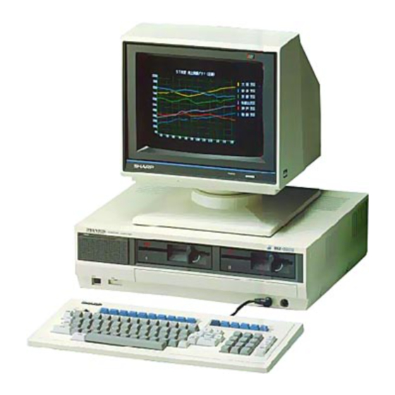
Page 2: Specifications
1-1. Specification of the main unit (Model 35XX) 1) High speed processing using multi-CPL' 2) Built in mini floppy disk 3) Built in printer interface and RS232C Aerial interface Outline 4) Connection of up to two video displa, mitt (separate graphic display or overlaid display possible on two individual color monitor units) 5) Permits the use of standard CP/M Model 3530 incluse a single double-side, double density mini floppy... - Page 3 Keyboard layout Refer to the page TIN "CIRCUIT DIAGRAM" 1-3. MZ-1U02 Expansion unit for the MZ-3500 series CPU, which can be attached to the rear side of the main unit. Optional boards are plugged in to the expansion box. Outline The expansion box will accomodate up to four option boards.
- Page 4 1-4. MZ-IR03 Optional board used graphic display functions with the Model-3500 series CPU. It includes 32KB of RAM. Outline It is inserted through the slot on the front panel of the PU. The MZ-1U02 expansion box is not required. vinrn HAM Specifications ~~~~~ Graphic functions...
- Page 5 MZ3500 1-6. MZ-1R06 Optional board for memory expantion of the MZ-3500 sries CPU. with this option the main memory (RAM) can be expanded Outline up to a maximum of 256 KB. This option plug into the expantion box in slot 1 or 3.
- Page 6 1-7. MZ-1D07 High resolution MZ 3500 series 12 green Outline Type Video tube Fluorescent color P39 (green, long PERSISTANCE) Total number of Display capacity display characters Specifications Display size 220 x 145 Method Input signals Horizontal Power supply 29W power consumpt Molded Cabinet Size (W x H x U...
- Page 7 MZ3500 1-8. System configuration of Model 3500 "Model-3541 = Model-3531 + MZ-1F03 Keyboard MZ-1K02 MZ-1K03 MZ-1K04 MZ-1K05 Printer IO2824E Option MFDI CE-331M |...
-
Page 8: Software (Memory) Configuration
2. SOFTWARE (MEMORY) CONFIGURATION Memory will be operated under four states of SDO ~ SD3, depending on the hardware and software configurations. In the paragraphs to follow, description will be made for those four states. MAIN CPU FFFF RAMA RAMA cooo BFFF RAMA... - Page 9 M 7. 3500 Operational description (1) Upon reset after power on, the main CPU loads the contents of the initial program loader (IPL) into RAM starting at address 4000H, during which time reset is applied to the sub-CPU. TIMING OF RESET SIGNAL Vtc- S Y S K E S - SKES-...
- Page 10 ROM-IPL 1. An 8KB ROM (2764 or mask ROM equivalent) is used for the ROM-IPL. 2. When the system reset signal turns from low to high state after power on, the main CPU starts to operate At this stage, the ROM-IPL is addressed. 3.
- Page 11 4000H-5FFFH. (2) As the main CPU loads the information from sector Communication between Main and SUB CPU 2:3. SD2 (ROM based BASIC) SD2 is active when "SHARP BASIC" is executed via ROM. M A S M A 2 BANK °...
- Page 12 2-4. SD3 (RAM based BASIC) SD3 is active when "SHARP BASIC" is ececuted via RAM. "SHARP BASIC" is loaded in RAM from the floppy disk. MAIN CPU BANK SELECT Ffft I I I RAMB gFFF RAMA ROM! ROM2 1FFF 0 0 0 0...
-
Page 13: Cpu And Memory
3-1. Block diagram 1) Relation between MMR (Main Memory Mapper) and main memory. , RAM (II'TION ' 6 4 K B V 2 ) J K » 2 K * Ml DM1 I MO*J OK II K U MO* 400 kl Mil I 1 ION si v i (.us... - Page 14 3-2. Main CPU and I/O port —££-1 v~\ r IORQ ADDRESS A7 A6 A5 A4 A3 A2 A1 AO • Connector I PC 2 |~^T "" f^-r-^r-. — r ~~> \J> -•> r DL \J I Obr (jtA. G2 B 0 MFUC •...
- Page 15 MZ3500 3-3. Sub CPU and I/O port *"" "MT 74LS138 2 3 4 5 6 7 8 9 A B C D E F AS 7654 £X\ 0000 0001 8251 S02 8253 0010 S03 8255 0011 S04 input port select 0100 0101 0110...
- Page 16 3-4. Memory mapper (MMR) SP6102R-001 1) Block diagram ADDRESS BUS AO . i. is. COAB COAB MKEQB RFSH I / O CONTROL BUS PORT MERQ LOGIC RFSH "WR DATA BUS I — \ DO-D7 INTB WAIT TIMING WAITB GENERATOR SYSR ->TO Memory mapping logic A 15...
- Page 17 AR13-AR15. This is means by which the 4 basic and CP/M memory maps are made, along with MS1 AR15 MSO. BASIC interpreter 32KB mask ROM chip select signal. Valid when SD2 is active (Sharp ROM based BASIC). Command (LDA 02H OUT 3FD) Internal MMR I/O port select logic signal. IOAB Goes low by the command IN/OUT #FC-#FF.
- Page 18 Polarity Pin No. IN/OUT Signal Name Main CPU 128KB dynamic RAM output buffer (LS244) output enable signal. RF1B Signal identical to R F 1 B RF2B Wait signal to the mam CPU (One wait cycle 15 applied during the memory fetch cycle of the main CPU. It consists of one clock WATB period) Chip select signal issued from the mam CPU to select the RAM shared by the main CPU and...
- Page 19 MX 3500 Polarity Pin No IN/OUT Signal Name System reset signal. SYSR Used to reset I/O port in the MMR. Input from the sytem assignment dip switch. "See the dip switch description, provided separately. Shared RAM select signal. COAB Address of the shared RAM is *F800-#FFFF for the main CPU Select signal for 8KB area allocated to slot 1.
- Page 20 MAIN CPU I/O PORT IN MEMORY MAPPER A D D K K S S A7 A6 A5|A4|A3|A2|Al|AO H E X UHUS 1 1 1 1 1 1 1 0 1 1 1 1 1 1 1 1 1. All output signals are reset to low level upon power on, except for SRBQ that goes high.
- Page 21 MZ3500 3-5. Memory (ROMIPL, RAMCOM, S-RAM) select circuit To main CPU 1) ROM-IPL select by the main CPU As ROM IPL turns to low level after power on address bus buffers (LS244, LS367) and data bus buffer (LS245) are enabled. S of the data selector 1C (LS157) is set to a low level to enable input 1A-4A.
-
Page 22: Crt Display
4-1. Specification 3KB (characit>-s! Display memory 96KB. max (graphic i Character display Screen structure 80 chrs x 25 lines. 80 chrs x 20 lines 40 chrs x 25 lines, 40 chrs x 20 lines Programmable 8 x 1 6 dots With lower case descenders Character 255 characters... - Page 23 Summary of video display specification High resolution CRT (640 x 400 dots mode) ^""~-\^ Type of monitor Green monitor Characters Graphics (option) Function ^^\^^ ASCII 8 x 1 6 Elements 8 x 20 Character s t r u c t u r e 5 x 1 4 80 x 25 mode Screen s t r u c t u r e...
- Page 24 1) Character display 1.1. Screen structure High resolution CRT Medium resolution CRT CRT used x 400 (640 dot) (640 fH = 20 9KHz ( N e w ) f V = 47 3Hz Character 80 x 25 lines 80 x 25 lines ASCIL 40 x 25 lines 40 x 20 lines...
- Page 25 MZ 3500 6) Screen overlay and displaying on two CRT's As there are two video output channels sible to display two independent screens on separate video display unit Overlay is possible on either Address ;p i (50) NOTE Both CRT1 and CRT2 must be high resolution CRT's (640 x 400) or medium resolution CRT's 'RO x Output to each CRT may be possible in the following combination .
- Page 26 7) ASCII CG Uses an 8KB MROM contains two patterns' 640 x 400 dots ( 8 x 1 6 dots) and 640 x 200 dots ( 8 x 8 dots) # O F F F 8 x 8 d o t pattern (2K byte) ! x 8 dot pattern (2K byte)
- Page 27 2) 20 line display mode Without line Graphic symbol 9) Cursor Sharp of the cursor: Same as seen in Model 3200 Reverse and blink) 10) Light pen input Incorporates the light pen input connector and its inter- face. The light pen, however, is an option.
- Page 28 2) Read/write from Z 80 to VRAM (1) Timing period for display and V-RAM Read/write. H • SYNC- BLNK- (2) Timing that the Z-80 can read/write VRAM The Z-80 can read/write VRAM when GDC FIFO buffer is either empty or Full, and can be accessed by 3) Structure of character VRAM (1) When read/write from GDC #07FF...
- Page 29 MZ3500 4) Graphic V R A M memory (MZIR03) • Block Diagram 1. read/write Mode The select signal RASA, RASB and RASC are generate from RAS, A14 and A1 5 which is signal of GDC-2. The address is allocated to each area selected by above signal. Read/write by Z-80 via the GDC (1) 640 x 200 dots display mode byte...
- Page 30 (2) 640 x 400 dots display mode Option I ( 4 8 K b y t e ) # 4 0 0 0 16 bits structure # 3 KKK * 0 0 0 0 B F F F Option II (96K byte) 16 bits s t r u c t u r e # 8 0 0 0...
- Page 31 MZ3500 (2) 640 x 400 bits display mode fH = 20.92 kHz fV = 47.3 Hz Dot clock (OD) 2XCCLK Horizontal display time Vertical display time Total rasters: 441 rasters Display rasters 400 rasters (3) CRT synchronizing signal specification (400 raster CRT) 1.
- Page 32 0 For 40 digit display CH48 - 1 : For 80 digit display There is a 40/80 digit switching signal I/O port in the gate array of CSP1 and CSP2, but, the I/O signal called CH48 is provided apart from the I/O port.
- Page 34 4/6. Master slice LSI (CSP-1) SP6102C 002 signal description Priority Signal Name HSYi Horizontal synchronizing signal from the GDC1 Also, it becomes the refresh timing signal in the dynamic RAM mode. NABC Input from the UPD7220 GDC1. When the GDC1 is in the character display mode, the attribute, blinking timing and line counter ciear signals are multiplexed.
- Page 35 MZ3500 CSP-1 Block Diagram 4 ,. .. MkRO (bO) DSO ' Jl J, „ o > — H — I)S2 — HSYI NABC FYD2 BLNK DSP2 "\ "N AT 2 n F/F l-» D F/F AT 4 1 i > n F/F »...
- Page 36 46. LSI (CSP-2) SP6012C-003 Signal Description Polarity IN/OUT Signal Name HSY2 Horizontal synchronizing signal from GDC2 which also becomes the refresh tirniny . i j r . s ' i in the dynamic RAM mode. BLK2 Erase signal input from the GDC2 which is supplied 4T the following times: 1.
- Page 37 >00 P r i o r i t y Signal Name Clock input 32MHz, 200 raster Graphic DRAM address multiplexer signal (High order 8 bits I ADS ADI 5] /low 3'der S hi" |ADO A D 7 ] select signal ) DSP2 Display timing signal (In the CSP 2, the signal BLINK from GDC2 is delayed by 2 collor intervals to create this signal )
- Page 38 4-7. GDC (Graphic display controller) (UPD7220) signal description Polarity Signal Name 2XCCLK Double character clock supplied from the external dot timing generator which has the followin^ two modes: 1. Character display mode 2. G DBIN Memory contro signal supp'ied to the image memory from the GDC, which causes the image memory output data to be sent on the data bus.
- Page 39 M Z 3500 Polar, ty IN/OUT Pin No Signal Name AD13ILCO)- IN/OUT Provides the following functions based on the operational mode of the GDC (graphic display mode, 35-37 character display mode 0, character display mode 1). AD15ILC2) 1. In the graphic display mode and character display mode 0: Bidirectional address/data bus 2.
- Page 40 4 8 CG Address Select Circuit ASCII C.G. Structure » I i r r =^=^ 1020 10! 1- Character Code 01 leBytes 8 x 1 6 dot Model 3500 > Pattern 400 Rasters lOOh Character Code 00 ifiBytes Model 3500 \ l'= I - 1000 01-1^...
- Page 41 MZ 3500 4-9. VSYNC From (8255 PB7) CH48 [Circuit description] When more than two UPD7220 GDC's are to be operated in parallel, one must be assigned to the master and the other to the slave in order to mantain synchronous display timing.
- Page 42 4-10. Character VRAM select circuit The signal BLNK is used to address the ASCII RAM within address area of 0000-07FF in transferring the display data from the VRAM to the CG. BL'SC BLNK Erase signal 6 I 1 6 > 2 K » 8 ) ASL C V - K A M 8bil...
- Page 43 MZ3500 4-12. Read/write from the Z-80 to V-RAM Read/write of the Model 3500 V-RAM is done via the UPD7220GDC. There are two methods used to read/write data. The method (1) is used for the model 3500. Set GDC command code Set parameter for the command Set parameter for the command.
- Page 44 (Subroutine lo send command and parameter to the GDC via the F I F O ) Example of graphic drawing by GDC 1) Dot display 0000 0001 0027 0028 HL reg — First address of the command code oarametpr B. reg — Q'ty of data. C reg - 60H (graphic GDC), 70H (character GDC) >...
- Page 45 M23500 [Explanation] C-COMMAND CODE p_ PARAMETER Display dot, specify the display address of the VRAM and the dot address. Set the command code of the SET mode (set mode plus CLEAR, REPLACE, and COMPLEMENT modes using "WRITE", and specify to "VECTE".
- Page 46 2) Straight line drawing 00000 0001 0027 0028 0050 Example to draw a straight line from (X, Y) = (3, 1) to (X, Y) = (635, 1). Coordinates must be changed to absolute addresses. (3, 1) - absolute address = 0028H Dot address = 2H Displacement between two points when the line draw direction is OA (to the right): X = 635-3 = 632 (=278H),...
-
Page 47: Mfd Interface
M Z 3500 5-1. Outline Floppy disk is a disk which is made of a mylar sheet whose surface is coated with magnetic particles and set on the device to write and read data on the surface of the disk It will be necessary to know operating pnciple of the floppy disk unit and operational description, including recording method and format. - Page 48 Example 2: CE330S (light passing through the notch is sensed and decoded as write protect) (Double side, Double density) Write enabled Front side Two types of write protection are used and attention must bepaid to the presience of the label because it may cause a wrong result if the label is used improperly.
- Page 49 MZ3500 o MFM method (double density) The MFM method writes data on the basis of the condi tion metntioned below, and it yields a data density two 0 £ 0 £ Input data \ /\ /\ X"V /\ / n n nnn n Write data The clock pulse (Ci will be eliminated in above illustra tion as there is no data preceding or following the clock...
- Page 50 Shown below is an enlarged view of sequence W r i t i n g starts as soon as the index hole comes through the index detect hole Sector 01 DATA < I N D E X Start point TT HH SS DL CRC CRC 7) Formatting To write the above format (ID section, data section, gap) on an entire surface of a new floppy disk is called...
- Page 51 MZ3500 5-3. MFD interface block diagram > MOTOT ON - 56 -...
- Page 52 FDC (UPD765) UPD765 pin configuration (top view) R L S t IQ »• OVcc » KDRW/SEEK »• K 3 L C T / D I R > *O FLTR/STEP > K3HDLD DBOo-« » « 0 READY DB1CX » O W P R X / 2 S 1 D E DB2O4 O FLT/TRKO DB304...
- Page 53 MZ3500 UPD765 signal description Signal name Pin No. RESET DB7 ~ DBO 1 3 - 6 DACK USD, 29,28 SYNC RW/SEEK HOLD SIDE LCT/DIR FLTR/STEP READY WPRT/2 SIDE INDEX FLT/TRKO WDATA WCLK Function Single phase, TTL level clock Set the FDC into an idle state, and all drive unit interface outputs, except PSO, 1 , and WDATA (don't care), are set to low level In addition, INT and DRW outputs are set to low level DB goes into an input state.
- Page 54 Signal name P,n No 32. 31 PSO. RDATA WINDOW 5-5. Data recording method There are two ways of recording data; FM recording method and MFM recording method. 2) MFM recording method (1) Data bit is placed in a middle of a bit cell. (2) When the data bit is "0", a clock bit is placed before the current bit cell.
- Page 55 M 7.3 500 5-7. Precompensate Circuit (Fig. 2) Not changed Not changed LATE(125»is) EARLY(125ja) (Table!) WDATA- 8MHz CLOCK EARLY- NOMAL- LATE- (Fig.3) The precompensate circuit is used to compensate the peak shift before writing. The FDC sends out the compensation rate to PSO and PS1 and the data bit location is shifted according to this signal.
- Page 56 In the case of the MFM method, need to trace cycle fluc- tuation is further increased, as a peak shift is apt to occur because there are three write data cycles. (Peak shift). Data read cycles fluctuate as the flux change point is moved forwards or backwards.
- Page 57 MZ3500 2) VFO circuit configuration READ — » DATA" The VFO circuit has the following capabilities. (1) Two modes: MFM and FM. (2) The VFO circuit operation is suspended during the SYNC field located before the ID field and data field. (3) After suspention, the VFO circuit will synchronize with the read data (timing is affected by a speed change in the FDD).
- Page 58 MFM Mode _rLTLJT_r A l M H z B)QA) Nomal Eary Delay ©...
- Page 59 MZ3500 A 4M B ( Q A ) C ( Q B ) D ( Q C ) WINDOW Normal Advanced Delayed Does not trace ± I FM mode timing chart...
- Page 60 ,— ^ "c — 0 2 - 8 « 1 £ CD" oinQle density ~^~^~ ~~^~~~ "o Q. J2 "O £ <u •£ "S'o "*" 1C *" T— 1 i. "6 O 4J i ui^ <u J: r "£ - ^J 2 r~ <—...
- Page 61 M/asoo Track 0, sector 1 information (SBACIS) (Fig 1) m media No of Track SIDE Sector sectors f 0 . Single density, other than front side, track 0. 1 . Double density, other than front side, track 0. . Side 0 (front side) SIDE = Side 1 (reverse side) No of data transfers INT=[IOCScapacity/1k] +1...
- Page 62 o Map information 0 track 9 sector 1 7H &0H 7 EH \ 127 \128 MAPNa Block NO Starting block number (directory) 0 track 10 sector I 71! 128 blocks are controlled by one sector. OOH-7FH 80H: End of link FEH: Links to next map, Indicates the byte position •...
- Page 63 MZ3500 o Block number allocation The program and data areas are located after Track 2 1 block = 2K bytes (8 sector) track Front B144 6145 B148 B149 2Kx 152 = 304K Each track is blocked in the following manner: 1 sector 1 block 15 sector...
-
Page 64: R232C Interface
6-1. General specification RS-232C bit serial input/output Input/output format 1 channel No of channels JIS 7-channel/JIS 8 channel Code used 110 to 9600 bits/sec Baud rate Half-duplex Transmission system Synchronization method Start-stop Communication control Non-procedure procedure Stop bif 1/1.5/2, with or without Data format even or odd parity. - Page 65 MZ3500 6-3. Block diagram of the interface 6-4. System switch functions ER signal is disabled. Causes an error when the ER signal is low or open during data output. The CD signal is set high Always high when power is while data output, but on to the main unit.
- Page 66 2) Data output control Stop S K N U 8251 AC Command instruction " L " - > K T S ( K T S , R X E N , T X E N ) »- 8251 AC Set counter (200ms) ERROR 101 Output data to The 8251 send data when CTS goes low.
- Page 67 M/3SOO 3) Data input control Waits for NMI by the RXRDY signal Resets error by setin DTR high Command instruction ( tK > 8251 AC ERROR R C V 8251 AC Command nstruction /Error reset ( E R . R X D I S L N ) \Data input disable/ 8251 AC...
- Page 68 6-6. 8253 Controls Baud rate of this interface will be determined by the clock output of the 8253. The 8251 is configured such that its baud rate is 1/16 of the input clock and has the following relation between the 8253 output clock and the baud rate: 8253 input frequency: 2457.6kHz 8253 Mode set: Mode 3(rec'angle waveform rate generator) Control signals...
- Page 69 M Z 3500 DO~D7 Data Bas Receive Data (IN/OUT) Write (IN) Read (IN) Control/Data (IN/OUT) Chip Select (IN) Data Set Ready (IN) Data Terminal Ready (OUT) Request to Send (OUT) Clear to Send (IN) T X R D Y . Transmitter Ready (OUT) Transmitter Clock (IN) .
- Page 70 8 2 5 1 D T K 8 2 5 1 Rl S chip address[0001/xxxx] TXRDY U i x OUT) RXRDY "RXC SYN/BD 8253 C L K O GATED OUTO 8 2 5 3 CLK1 chip address[0010/xxxx] GATE1 OUT1 # U x H 2 X H O U T # | CLK2...
-
Page 71: Printer Interface
M 7. 3500 7-1. Printer interfacing circuit AS 4 • AS 5 AS6 • AS 7 C h i p I )fi i >de r R I ) 3C r-— • ^ — ° I ORQ °^ * - ! - 'arallel interfacing signals IN/OUT Pin No. - Page 72 7-3. General description of the parallel interface The 8255 is used for the LSI to control the parallel inter- face. The 8255 can be set in the following mode. /PORT A: MODE 0 I P O R T B : MODE 1 C: Output Data transfer timing BUSY...
- Page 73 M / 3500 7-6. I/O port map 8255 ON SUB CPU BUS 8255 chip address(0011/xxxxj Group A: Mode 1 Group B: Mode 0 INPUT P O R T C 7 4 L S 2 4 4 7 4 L S 2 4 4 port address[0100/xxxx] # 4 X DATA8...
-
Page 74: Other Interface
8-1. Clock circuit 1) Schematic 2) Clock timing READ HOLD . READ mode mode mode Cn(CO~C2) WRITE HOLD mode mode Don't care DOUT Tens digit of seconds 8. OTHER INTERFACES " l«"-.r / ^Ones digit of seconds Tens digit of seconds Tens digit of month ' Tens digit of month* - 8) -... - Page 75 MZ3500 3) ^PD1990AC Block diagram OK O Command specification Command Register hold Register shift Time set Time read Input/output format Example: In the case of 10 o'clock, 25 minutes, 49 seconds, July 30th. (LSB) «- Seconds—' Description DOUT Holds 40-bit S/R Data input/output [LSB] Output of LSB Data of the 40-bit S/R is...
- Page 76 8-2. Voice input/output circuit Music output waveform • Tonal signal OUT1 • Sustain • 2SC458 emitter • 2SC458 collector Speaker • -Tlj output » GETE1 PD8255 mmmil - 83 -...
- Page 77 M/3500 Expansion and interrupt (See 3-(2)-4 for interrupt) 1) Options and expansion units Options not requiring expansion unit JIS keyboard MZ 1K01 1001 14" medium resolution color CRT 1D02 12" high resolution green CRT •1D03 1 2" high resolution color CRT -1S01 14"...
- Page 78 System SW1 (DIP SW) (User operative through the cabinet bottom) Position Function Signal name Printer select CRT select Choice of decimal point output format RS232C assign Key shift mode setup (SW8) Choice of CG for display (SW9) ^ = — = T Dip switches (A) and (B) located on the PWB are used for servicing the MFD or for other machine service and there fore the user is not supposed to use these switches...
- Page 79 MZ3500 DIPSW(B) DIP S W ( A ) ><^ Can be in either state Switches are set in this manner before shipment of machines this us the single-sided minifloppy disk drive. Switches are set in this manner before shipment of machines that use the double-sided minifloppy disk drive.
-
Page 80: Power Circuit Description
9, POWER CIRCUIT DESCRIPTION 1. BLOCK DIAGRAM A. +5V and +12V supplies 1. Functions a. Supply voltage is first rectified in the rectifier circuit and sent out to the switching regulator via the over- current detector provided in the overcurrent protect circuit. - Page 81 M 7,3500 Switching regulator + 5V (Switching regulator and constant voltage control circuit) « VR is the+5V or+12V adjusting VR. • is provided to discharge current from Cj after power off. - 88-...
- Page 82 c. Power switching circuit As the signal from the oscillator is amplified through Q7 to Q6 to change current to the transformer T2. it causes voltage to appear on the base of Q5 (one of components is cut by D1), so that the transistor Q5 begins to per- form switching operation in synchronization with the oscillation frequency.
- Page 83 MZ3500 10. MZ1K01 KEYBOARD CONTROLLER CIRCUIT DESCRIPTION 10-1. Specification of keyboard control 1) Input Buffer Capacity: 64 bytes • Key-in data is written to the input buffer first, and is supplied to the CPU, byte by byte. • When an overflow is detected, the overflow code is affired to the key-in data already sent, before being sent to the CPU.
- Page 84 10-2. Key search timing Single key entry STROBE 1 Strobe *~5.5ms M 5ms -» RETURN cvcle DATA OUT Two key entry Key 1 /A" Key 2 STROBE -5.5ms—M—•6.5ms —M—5ms —W DATA DATA 10-3. Key serial transmission procedure 1) Data format Key -»...
- Page 85 MZ 3500 • Command flag: "0" when succeedeing 8 bits are a key data. "1" when it is a command or a graphic control data. • Data: Positive logic (negative logic on the cable) • Parity: Odd parity up to 27 bit from the correction flag. 2) Interfacing signals •...
- Page 86 M?3500 10-4. Keyboard controller basic flow Power ON Timer START (5mS) - 93 -...
-
Page 87: Self Check Functions
MZ3500 10-5. keyboard controller signal description Porality IN/OUT signal name Output data signal from the sub CPU (D(O) XTAL1 Internal clock oscillator crystal input XTAL2 Internal clock oscillator crystal input RESET Processor initialize + 5V Strove of D(C) that also is used for interrupt to the keyboard side (ST(O) PSEN RETURN signal from the keyboard is input when a key is pushed during key search 0V supply... - Page 88 Type of error MDF 1/F error 1sec. 4sec. (2.1 SDO read/write error SDO bank alternation error ® AD2 bank alternation error © AD3 bank alternation error ROM sum-check error © Option RAM read/write error (Indicated even when the option RAM is not in use) /s~.
- Page 89 MZ 3500 Sector 1, Track 0 information TRACK SIDE SECTOR A A H Represent the Drive unit system media specification NO. OF SECTOR Single dencity (Track 0) Double density (other than Track 0) SIDE 0 (front side) SIDE SIDE 1 (reverse side) 11-2.
- Page 90 1) Memory test Sub-IOCS RAM (4000H-5FFF) Shared RAM (2003H-23FFH) Shared RAM (2440H-27FFH) Above are tested. [Display] (1) Normal test ending RA OK: SUB-IOCS RAM RA OK Shared RAM RA OK Above information are displayed on three display lines. (2) Abnormal test ending 3) CRT inter face test Performance of the CRT is tested.
- Page 91 MZ3500 ( Check No. 4 ) Border in black !• "H" in whi ( Check No. 6 ) Backroung in red L "H" in blue L "H" in green [• "H" in white 4) Speaker test Performance of the speaker and the volume control are tested.
- Page 92 8) ROM-IPL MAIN CPU CHECKER FLOW CHART 1/2 MAIN CUP CHECKERSTAHT Write "66" »nd~Of~ on Tracki 0.20.»^3 NOTE lnclud« SEEK etroi and RECALIBRANTE NOTE tr»c1i>d« SEEK error and RECALIBRATE - 99- MZ3500...
- Page 93 MZ3500 MAIN CPU CHECKER FLOW CHART Option HAM read/write check Change bank of the option RAM - 100 - Error on display HALT...
- Page 94 M 7*500 SUB CPU CHECKER FLOW CHART 1/3 SUB CPU CHECKER START CRTmt*f face t«t SeiGDCto«00<amr. - 101 -...
- Page 95 MZ3500 SUB CPU CHECKER FLOW CHART 2/3 th» timer to 23 hourt. minuiei. 58 **corxii *mb«r 3 III Printer int M»c* tt»t SUB CPU CHECKER FLOW CHART 3/3 11-3. Keyboard unit test functions 1) Keyboard controller ROM test (1) After power on in a normal condition, it starts to carry out the ROM self-test.
-
Page 96: Ipl Flow Chart
12-1. MAIN CPU IPL FLOW CHART 1/2 MAIN CPU (PL START Transfer the program m 1000E-J0400E-. ROM/RAM test S**ect memory location SUM IPL START Check MFD Index itgnal 12. IPL FLOW CHART Jump to 400EH Contents of parameter sector 1. Kind of MFD Single-side dencity. - Page 97 MZ3500 MAIN CPU IPL FLOW CHART 2/2 Check if IOCS program area is smaller than RAM volume. LOAD IOCS SEEK& READ Transfer the IOCS program to shared RAM 8000H~-»-F800H~ LOAD BOOT LOAD BOOT SSEK& READ JUMP BOOT ADDRESS I/O SYSTEM LOAD ERROR transfer HALT...
- Page 98 Rest GDC Check ROM sum Initialize GDC and check G VRAM Set the custom LSI CSPI and CSP2 control boards Initialize GDCagatr C-GDC, G-GDC command transfer IPL ROM is broke u indicated on display HALT CUP STOP - 105 - MZ-3500...
- Page 99 13-18. PIN CONFIGURATION OF 1C & LSI 74 LS 00 « H m R R R R R F1 LJ LJ U U U LJ U ^> LJ LiJ LiJ LJ LL! LiJ LJ 74 LS 03 LJ LJ LJ LJ LJ LJ LJ 74 tS 04 LJ LJ LJ LJ LJLJ LJ CM>...
- Page 100 M 7. - 3500 LJLJLJliJLJULJ 1 Ml 74 LS 367 ("- «A LJ LiJ LJ bJ LJ LUTJ TZT E N A B L E bJ LJ LU U LiJ LiJ OLTPbT JQ CONTROL LJ U U LT .,-. C I R ENABLE /<J LU LU U LJ LlJ LJ U U...
- Page 101 / " P D 8 2 5 1 D»i i ' - C I.2C K M . C ^ R V T I M C M>C DIM R DKT^ ""'C J D S K I > l C I X . Q I-7C "~K I K (_ I H 0 f"~...
-
Page 102: Parts List & Guide
MZ-35OO PARTS GUIDE LI... - Page 103 MZ-3500 li Exteriors PRICE PARTS CODE RANK MARK C C A B C 1 0 0 7 A C Z Z G F T A F 1 0 0 1 A C Z Z H B D G B 3 0 0 4 G E S A...
- Page 104 IE--or ooss-zw...
- Page 105 MZ-3500 [2] PWB & Fixing angles PRICE PARTS CODE RANK MARK J K N B M 0 0 0 4 P A Z Z L A N G S 1 0 0 6 A C 2 Z L A N G K 1 0 0 7 A C Z Z...
- Page 106 13. Connector PRICE PARTS CODE RANK MARK O C N C P 6 0 4 1 Q C Z Z Q C N C P 4 8 4 1 Q C Z Z Q C N C W 1 0 0 1 A C Z Z Q C N C M 1 0 0 4 A C Z Z QC N W- 1 0 0 7 AC Z Z QCN CWO 2 0 7 HC Z Z...
- Page 107 MZ-3500 [41 Others PRICE PARTS CODE RANK MARK R M E M R 1 0 0 4 A C 0 7 U B N D A 1 0 0 8 C C Z Z S P A K A 1 0 0 3 A C Z Z...
- Page 108 Transistor (2SA733-Q) Transistor (2SA733-Q) Transistor (2SA1 020- Y) Transistor (2SC2334-L) Transistor (2SC2655-Y) Transistor (2SC1815-Y) Transistor (SI OSC4M) Zener diode (H29L-A1) Diode (1S234-8H) Zener diode (HZ11L-B1) Zener diode (HZ7L-C2) MZ-3500 [M001] [Q001] [Q002] [Q003] [0004] [Q005] [Q006] [0007] [Q008] [Q009] [Q010]...
- Page 109 MZ-3500 [6j Power supply unit PRICE PARTS CODE RANK MARK O A E 3 0 1 2 1 9 2 1 X X O A E 3 0 1 2 1 9 2 1 / / O A E 3 0 3 7 9 0 2 9 / /...
- Page 110 M2-3500 J9, MZ1K02,1K03,1K04,1K05 (Key unit) i <,...
- Page 111 MZ-3500 [1Q! MZ1R03 (Graphic board) PRICE PARTS CODE RANK MARK D U N T K 1 0 2 5 A C Z Z S P A K A 1 0 1 3 A C Z Z S P A K C 1 0 7 8 A C Z Z...
- Page 112 R V R - A 5 4 5 2 Q C Z Z R V R - M C 3 2 1 Q C Z Z I S ] S P A K A 1 0 0 3 A C Z Z MZ-3500 PRICE PART RANK...
- Page 113 MZ-3500 PRICE PART PARTS CODE MARK RANK RANK S P A K A 0 04 A C Z Z 9- 109 S P A K A 0 0 9 A C Z Z 9- 110 S P A K A...
- Page 114 OAE 2 3 594 924// O A E 3 0 1 0 9 0 6 6// OAE 30 1 1 67 29// O A E 3 0 1 2 0 4 56// OAE 30 1 20524// MZ-3500 PRICE PART RANK MARK...
- Page 115 MZ-3500 PRICE PART PARTS CODE RANK MARK RANK O A E 3 0 1 20524// 6- 65 6- 66 6- 44 O A E 3 0 1 206 5 O// O A E 3 0 1 2 1 8 6 6//...
- Page 116 SHARP CORPORATION Industrial Instruments Group Reliability & Quality Control Department Yamatokoriyama, Nara 639-11, Japan 1983 January Printed in Japan s...