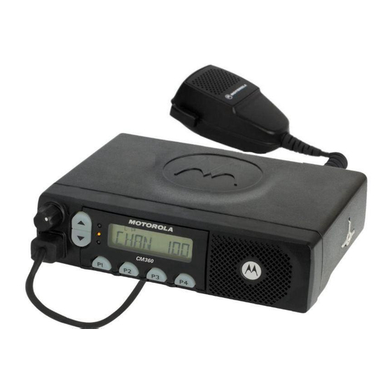
Motorola CM160 Service Information
Commercial series cm radios uhf1 (403-440mhz) high power
Hide thumbs
Also See for CM160:
- User manual (46 pages) ,
- Basic user's manual (12 pages) ,
- Service information (90 pages)

Related Manuals for Motorola CM160


Summary of Contents for Motorola CM160
- Page 1 Commercial Series CM Radios UHF1 (403-440MHz) High Power Service Information Issue: October 2004...
- Page 2 Accordingly, any copyrighted Motorola computer programs contained in the Motorola products described in this manual may not be copied or reproduced in any manner without the express written permission of Motorola. Furthermore, the purchase of Motorola...
-
Page 3: Table Of Contents
Table of Contents Chapter 1 MODEL CHART AND TECHNICAL SPECIFICATIONS 1.0 CM160 Model Chart.....................1-1 2.0 Technical Specifications ..................1-2 Chapter 2 THEORY OF OPERATION 1.0 Introduction ......................2-1 2.0 UHF (403-440MHz) Receiver ................2-1 2.1 Receiver Front-End ..................2-1 2.2 Receiver Back End ..................2-2 3.0 UHF Transmitter Power Amplifier (403-440 MHz) ..........2-2... - Page 4 8.3 Dual Tone Multiple Frequency (DTMF) Data ..........2-18 9.0 Receive Audio Circuits..................2-19 9.1 Squelch Detect ..................... 2-19 9.2 Audio Processing and Digital Volume Control..........2-20 9.3 Audio Amplification Speaker (+) Speaker (-) ..........2-20 9.4 Handset Audio....................2-21 9.5 Filtered Audio and Flat Audio ...............
-
Page 5: Model Chart And Technical Specifications
Chapter 1 MODEL CHART AND TECHNICAL SPECIFICATIONS Model Chart (UHF1 403-440 MHz - High Power) CM Series UHF1 403-440 MHz Model Description MDM50QPF9AA2_N CM160 403-440 MHz 25-40W 64-Ch Item Description PMUE2160_ S. Tanapa UHF1 40W 64 Ch BNC FCN5523_ Control Head... -
Page 6: Technical Specifications
UHF1 Frequency Range: 403-440 MHz Frequency Stability ±2.5 PPM (-30°C to +60°C, 25°C Ref.) Channel Capacity: CM160 - 64 Channel Spacing: 12.5/25 kHz Power Supply: 13.6 Vdc (10.88 Vdc - 16.32 Vdc) negative Vehicle ground 4.65” X 6.67” X 1.73”... - Page 7 Technical Specifications Transmitter Specification UHF1 Power Output 25-40W Conducted/Radiated -36 dBm < 1 GHz Emissions: -30 dBm > 1 GHz Audio Response: (from 6 dB/ oct. Pre-Emphasis, 300 to +1, -3dB 3000Hz) Tx Audio Distortion < 3% Modulation Limiting: ±2.5 kHz @ 12.5 kHz ±4.0 kHz @ 20 kHz ±5.0 kHz @ 25 kHz FM Hum and Noise:...
- Page 8 MODEL CHART AND TECHNICAL SPECIFICATIONS THIS PAGE INTENTIONALLY LEFT BLANK...
-
Page 9: Theory Of Operation
Chapter 2 THEORY OF OPERATION Introduction This Chapter provides a detailed theory of operation for the UHF circuits in the radio. Details of the theory of operation and trouble shooting for the the associated Controller circuits are included in this Section of the manual. -
Page 10: Receiver Back End
THEORY OF OPERATION Receiver Back End The IF signal from the crystal filter enters the IF amplifier which provides 20 dB of gain and feeds the IF IC at pin 1. The first IF signal at 44.85 MHz mixes with the second local oscillator (LO) at 44.395 MHz to produce the second IF at 455 kHz. -
Page 11: Power Controlled Driver Stage
UHF Transmitter Power Amplifier (403-440 MHz) PA.Op-amp U103-3 monitors the drain current of U101 via resistor R122 and adjusts the bias voltage of U101. In receive mode, the DC voltage from RX_EN line turns on Q101, which in turn switches off the biasing voltage to U101. -
Page 12: Harmonic Filter
THEORY OF OPERATION Harmonic Filter Inductors L111, L113 and L128 along with capacitors C1011, C1023, C1020, C1016, C1025 and C1026 form a low-pass filter to attenuate harmonic energy coming from the transmitter. Resistor R150 along with L130 drains any electrostatic charges that might otherwise build up on the antenna. The harmonic filter also prevents high level RF signals above the receiver passband from reaching the receiver circuits to improve spurious response rejection. -
Page 13: Fractional-N Synthesizer
UHF (403-440MHz) Frequency Synthesizer parameters (four characterize the inverse Bechmann voltage curve and one for frequency accuracy of the reference oscillator at 25 degrees C). This algorithm is implemented by the LVFRAC-N (U200) at the power up of the radio. TCXO Y200, along with its corresponding circuitry R204, R205, R210, and C2053, are not placed as the temperature compensated crystal proved to be reliable. -
Page 14: Voltage Controlled Oscillator (Vco)
THEORY OF OPERATION Voltage Controlled Oscillator (VCO) The Voltage Controlled Oscillator (VCO) consists of the VCO/Buffer IC (VCOBIC, U201), the TX and RX tank circuits, the external RX buffer stages, and the modulation circuitry. AUX3 (U200 Pin 2) U200 Pin 32 Prescaler Out TRB IN Pin 20... -
Page 15: Synthesizer Operation
UHF (403-440MHz) Frequency Synthesizer Synthesizer Operation The synthesizer consists of a low voltage FRAC-N IC (LVFRAC-N), reference oscillator, charge pump circuits, loop filter circuit, and DC supply. The output signal (PRESC_OUT) of the VCOBIC (U201, pin 12) is fed to the PREIN, pin 32 of U200 via a low pass filter which attenuates harmonics and provides a correct input level to the LVFRAC-N in order to close the synthesizer loop. -
Page 16: Controller Theory Of Operation
THEORY OF OPERATION Controller Theory of Operation This section provides a detailed theory of operation for the radio and its components. The main radio is a single-board design, consisting of the transmitter, receiver, and controller circuits. A control head is connected by an extension cable. The control head contains LED indicators, a microphone connector, buttons, and speaker. - Page 17 Controller Theory of Operation The DC voltage applied to connector P2 supplies power directly to the following circuitry: • Electronic on/off control • RF power amplifier • 12 volts P-cH FET -U514 • 9.3 volt regulator • Audio PA Ignition Control Head RF_PA, 8.5A Audio_PA...
-
Page 18: Protection Devices
2-10 THEORY OF OPERATION Voltage regulator U503 provides 5V for the RF circuits. Input and output capacitors are used to reduce the high frequency noise and provide proper operation during battery transients. VSTBY is used only for CM360 5-tone radios. The voltage VSTBY, which is derived directly from the supply voltage by components R5103 and VR502, is used to buffer the internal RAM. -
Page 19: Microprocessor Clock Synthesiser
Controller Theory of Operation 2-11 5.3.3 Emergency Mode The emergency switch (P1 pin 9), when engaged, grounds the base of Q506 via EMERGENCY _ACCES_CONN. This switches Q506 to off and consequently resistor R5020 pulls the collector of Q506 and the base of Q506 to levels above 2 volts. Transistor Q502 switches on and pulls U501 pin2 to ground level, thus turning ON the radio. -
Page 20: Serial Peripheral Interface (Spi)
2-12 THEORY OF OPERATION Serial Peripheral Interface (SPI) The µP communicates to many of the IC’s through its SPI port. This port consists of SPI TRANSMIT DATA (MOSI) (U403-pin100), SPI RECEIVE DATA (MISO) (U403-pin 99), SPI CLK (U0403-pin1) and chip select lines going to the various IC’s, connected on the SPI PORT (BUS). This BUS is a synchronous bus, in that the timing clock signal CLK is sent while SPI data (SPI TRANSMIT DATA or SPI RECEIVE DATA) is sent. -
Page 21: Normal Microprocessor Operation
Controller Theory of Operation 2-13 Normal Microprocessor Operation For this radio, the µP is configured to operate in one of two modes, expanded and bootstrap. In expanded mode the µP uses external memory devices to operate, whereas in bootstrap operation the µP uses only its internal memory. -
Page 22: Static Random Access Memory (Sram)
2-14 THEORY OF OPERATION Static Random Access Memory (SRAM) The SRAM (U402) contains temporary radio calculations or parameters that can change very frequently, and which are generated and stored by the software during its normal operation. The information is lost when the radio is turned off. The device allows an unlimited number of write cycles. -
Page 23: Transmit Audio Circuits
Transmit Audio Circuits 2-15 Transmit Audio Circuits 24kOhms TX SND TX RTN U509 CONTROL HEAD FILTERS AND CONNECTOR PREEMPHASIS ASFIC_CMP GCB3 U504 LIMITER HS SUMMER EXT MIC U509 SPLATTER FLAT TX FILTER AUDIO MOD IN ACCESSORY LS SUMMER CONNECTOR SECTION GCB5 (SYNTHESIZER) ATTENUATOR... -
Page 24: Ptt Sensing And Tx Audio Processing
2-16 THEORY OF OPERATION 7.1.2 Standard Microphone Hook Pin is shorted to the hook mic inside the standard Mic, If the mic is out off hook, 3.3V is routed to R429 via R458, D401, and it create 0.7V on MIC_SENSE (u.P U403-67) by Voltage Divider R429/R430. -
Page 25: Transmit Signalling Circuits
Transmit Signalling Circuits 2-17 Transmit Signalling Circuits SUMMER 5-3-2 STATE HIGH SPEED ENCODER CLOCK IN SPLATTER (HSIO) FILTER DTMF MICRO ENCODER CONTROLLER U403 ASFIC_CMP U504 LOW SPEED ENCODER SUMMER CLOCK IN (LSIO) TO RF ATTENUATOR SECTION MOD IN (SYNTHESIZER) Figure 2-8 Transmit Signalling Path From a hardware point of view, there are 3 types of signaling: •... -
Page 26: High Speed Data
2-18 THEORY OF OPERATION High Speed Data High speed data refers to the 3600 baud data waveforms, known as Inbound Signaling Words (ISWs) used in a trunking system for high speed communication between the central controller and the radio. To generate an ISW, the µP first programs the ASFIC CMP (U504) to the proper filter and gain settings. -
Page 27: Receive Audio Circuits
Receive Audio Circuits 2-19 Receive Audio Circuits ACCESSORY CONNECTOR FLT RX AUDIO AUDIO SPKR + EXTERNAL SPKR - U502 SPEAKER SPKR+ SPKR- CONTROL HEAD CONNECTOR MUTE U509 INTERNAL SPEAKER HANDSET AUDIO U505 GCB4 U IO AUDIO URX OUT GCB1 VOLUME AUX RX ASFIC_CMP ATTEN. -
Page 28: Audio Processing And Digital Volume Control
2-20 THEORY OF OPERATION Audio Processing and Digital Volume Control The receiver audio signal (DISC AUDIO) enters the controller section from the IF IC where it is.DC coupled to ASFIC CMP via the DISC input U504-pin 2. The signal is then applied to both the audio and the PL/DPL paths The audio path has a programmable amplifier, whose setting is based on the channel bandwidth being received, an LPF filter to remove any frequency components above 3000Hz, and a HPF to... -
Page 29: Handset Audio
Receive Signalling Circuits 2-21 Handset Audio Certain handheld accessories have a speaker within them which require a different voltage level than that provided by U502. For these devices HANDSET AUDIO is available at control head connector J2 pin18. The received audio from the output of the ASFIC CMP’s digital volume attenuator is routed to U505 pin 2 where it is amplified. -
Page 30: Alert Tone Circuits
2-22 THEORY OF OPERATION The low speed limited data output (PL, DPL, and trunking LS) appears at U504-pin18, where it connects to the µP U403-pin 80. The low speed data is read by the µP at twice the frequency of the sampling waveform; a latch configuration in the ASFIC CMP stores one bit every clock cycle. -
Page 31: Troubleshooting Charts
Chapter 3 TROUBLESHOOTING CHARTS This section contains detailed troubleshooting flowcharts. These charts should be used as a guide in determining the problem areas. They are not a substitute for knowledge of circuit operation and astute troubleshooting techniques. It is advisable to refer to the related detailed circuit descriptions in the theory of operation sections prior to troubleshooting a radio. -
Page 32: Troubleshooting Flow Chart For Receiver Rf (Sheet 1 Of 2)
TROUBLESHOOTING CHARTS Troubleshooting Flow Chart for Receiver RF (Sheet 1 of 2) START Problem No (Either 12.5K or 25K channel spacing having problem) in 12.5 KHz and 25 KHz channel spacing 9V on Go to to U301 Check R310 (LNA) DC Section Go to RX_EN... -
Page 33: Troubleshooting Flow Chart For Receiver (Sheet 2 Of 2)
Troubleshooting Flow Chart for Receiver RF (Sheet 1 of 2) Troubleshooting Flow Chart for Receiver (Sheet 2 of 2) From Check visually all receiver Go to (IFIC -Vcc) components DC Section OK ? installation ? Inject - 40dBm (CW) Check to RF connector Installation the component... -
Page 34: Troubleshooting Flow Chart For 40W Transmitter (Sheet 1 Of 3)
TROUBLESHOOTING CHARTS Troubleshooting Flow Chart for 40W Transmitter (Sheet 1 of 3) START No or too low power when keyed Check components between >4A Current >500mA & <4A Q100 and RF output, increase when Antenna Switch D104, keyed? D103, VR102 and Q106 <500mA Control Check PA... -
Page 35: Troubleshooting Flow Chart For 40W Transmitter (Sheet 2 Of 3)
Troubleshooting Flow Chart for 40W Transmitter (Sheet 1 of 3) Troubleshooting Flow Chart for 40W Transmitter (Sheet 2 of 3) Check PA Stages No or too low power when keyed Voltage Check U510 at Q101 & Q102 Check Q102, base=0? Q101, R122, R165 Check resistive network at Voltage at... -
Page 36: Troubleshooting Flow Chart For 40W Transmitter (Sheet 3 Of 3)
TROUBLESHOOTING CHARTS Troubleshooting Flow Chart for 40W Transmitter (Sheet 3 of 3 Check Final PA Stage Check components PA_Bias Supply Voltage between ASFIC & Voltage at Replace Q100 Q100 before re- R134 placing Q100 2.11V 1-4V RF Voltage after C1044 >0.36mV? RF Voltage Check FGU... -
Page 37: Troubleshooting Flow Chart For Synthesizer
Troubleshooting Flow Chart for Synthesizer Troubleshooting Flow Chart for Synthesizer Start 3.3V Check 3V at U200 Regulator pins 5, 20, 34 U503 & 36 Visual Correct check of the Problem Board Check D200, D201, C2026, C2025, & C2027 16.8MHz 16.8MHz Replace signal at U200 Pin 47... -
Page 38: Troubleshooting Flow Chart For Vco
TROUBLESHOOTING CHARTS Troubleshooting Flow Chart for VCO Low or no RF Signal Low or no RF Signal TX VCO RX VCO at input to PA at TP1 Visual check Visual check Correct of board of board Problem Make sure Synthesizer is 4.5V DC 4.5V DC working correctly and runner... -
Page 39: Troubleshooting Flow Chart For Dc Supply (1 Of 2)
Troubleshooting Flow Chart for DC Supply (1 of 2) Troubleshooting Flow Chart for DC Supply (1 of 2) Since the failure of a critical voltage supply might cause the radio to automatically power down, supply voltages should first be probed with a multimeter. If all the board voltages are absent, then the voltage test point should be retested using a rising-edge-triggered oscilloscope. -
Page 40: Troubleshooting Flow Chart For Dc Supply (2 Of 2)
3-10 TROUBLESHOOTING CHARTS Troubleshooting Flow Chart for DC Supply (2 of 2) D3_3V Check VDC on C5007 Go to Digital Section Check Voltage on V=3.3V C5041 Replace U510 Go to Start 9v<V<9.8v... -
Page 41: Allocation Of Schematics And Circuit Boards
Chapter 4 UHF1 PCB/ SCHEMATICS/ PARTS LISTS Allocation of Schematics and Circuit Boards UHF1 and Controller Circuits The UHF circuits are contained on the printed circuit board (PCB) which also contains the Controller circuits. This Chapter shows the schematics for both the UHF circuits and the Controller circuits. The PCB component layouts and the Parts Lists in this Chapter show both the Controller and UHF circuit components. - Page 42 UHF1 PCB/ SCHEMATICS/ PARTS LISTS THIS PAGE INTENTIONALLY LEFT BLANK...
-
Page 43: Uhf1 25-40W Pcb 8486577Z02 / Schematics
UHF1 25-40W PCB 8486577Z02 / Schematics UHF1 25-40W PCB 8486577Z02 / Schematics VREV_BUFFER_IN VREV_BUFFER_IN TX_INJ TX_INJ FILT_SW_B+ FILT_SW_B+ PA_BIAS PA_BIAS COMPARTMENT MAIN COMP_B+ COMP_B+ DET_VFWD DET_VFWD PWR_SET PWR_SET INTEGRATOR INTEGRATOR RX_EN RX_EN TX_EN TX_EN PA_CURRENT PA_CURRENT UHF 1 Interconnection between Main Board and Power Amplifier Compartment... - Page 44 UHF1 25-40W PCB 8486577Z02 / Schematics C110 R101 C1088 C1113 C1037 C5100 R197 C1097 R195 C1001 C1008 C1004 C1026 C1283 C1025 VR693 C5004 R196 C1095 Q104 VR501 C1252 VR500 L130 L126 C1251 C1114 R199 C1017 C1267 C1098 C1154 R5082 L111 R187 L120 R5081...
- Page 45 UHF1 25-40W PCB 8486577Z02 / Schematics R113 C1112 R110 C1089 C5000 R129 R114 C1055 C5086 R127 C1061 VR692 R128 D402 L117 R126 C1106 R150 C1002 R403 R175 R404 R147 C1073 L124 R131 VR503 C5083 L121 R184 R405 R421 R134 C1027 L500 R5049 D100...
- Page 46 UHF1 25-40W PCB 8486577Z02 / Schematics FILT_SW_B+ D3_3V FILT_SW_B+ D3_3V TX_EN SPI_CLK SPI_MOSI SPI_MISO RX_EN LOC_DIST RSSI SYNTH_CS SYNTH_LOCK ASFIC_CS CH_ACT SQ_DET LSIO HSIO F1200 uP_CLK DIGITAL VS_AUDIO_SEL RESET J3 - DNP D3_3V VS_INT J3-17 SERIAL CLOCK VOICE STORAGE AUDIO SELECT J3-4 VS_RAC J3-16...
- Page 47 UHF1 25-40W PCB 8486577Z02 / Schematics RX_EN TX_EN (SOURCE) (SOURCE) (SOURCE) 3V D3_3V 5V COMP_B+ D3_3V COMP_B+ PA_CURRENT PA_CURRENT SPI_MOSI PA_BIAS PA_BIAS SPI_CLK PWR_SET PWR_SET FILT_SW_B+ ASFIC_CS (SOURCE) FILT_SW_B+ CH_ACT FILT_SW_B+ SQ_DET (SOURCE) LSIO HSIO DC & AUDIO VREV_BUFFER_IN F1200 VREV_BUFFER_IN FILT_SW_B+ uP_CLK...
- Page 48 UHF1 25-40W PCB 8486577Z02 / Schematics (SOURCE) Place inside of the PA compartment PA_FILT_B+ L100 IF108 LOAD_3 57R01 2113740F57 L119 57R01 C1053 COMP_B+ 180.p IF109 C1116 R137 39.p C1115 C1099 C1100 39.K FLT_9V C1000 C1112 C1111 C1110 C1109 C1106 C1089 C1103 FILT_SW_B+_PA C1107...
- Page 49 UHF1 25-40W PCB 8486577Z02 / Schematics R132 100K PA_CURRENT C1095 LM2904 39pF R111 U102 R114 R177 0662057A49 0662057A73 5113818A01 FINAL_CURRENT_SENSE C1055 R113 C1056 FILT_SW_B+_PA 120.p 120.p 120.p 0662057A73 C1073 R110 R115 0662057A49 0662057B05 R112 R101 200K C110 0662057A73 1.639m 120.p R116 Current sense protection(option) LOAD_2...
- Page 50 4-10 UHF1 25-40W PCB 8486577Z02 / Schematics L217 390nH C2000 C2034 C2015 R225 2.2uF C2026 120.p 0.1uF 150. C2025 R228 100. C2055 D200 L200 C2016 C2004 C2024 390nH 0.1uF 2.2uF R226 C2005 C2023 C2035 150. 120.p 2.2uF C2027 C2198 D201 R202 C2013 C2001...
- Page 51 UHF1 25-40W PCB 8486577Z02 / Schematics 4-11 V_SF L201 R231 680nH C2009 100n C2040 C2038 C2007 C2011 120.p 120.p 0.1uF C2008 C2042 C2041 0.1uF R235 0.1uF 120.p 120.p R220 L209 510. 100.0n V_SF L208 100.0n C2010 C2039 100n 120.p C2021 R215 R216 L202...
- Page 52 4-12 UHF1 25-40W PCB 8486577Z02 / Schematics FRONT-END SHIELD R334 Q304 Q306 430. C321 R346 LOC_DIST 10.K R300 R310 120.p MIXER SHIELD L304 10.K 15.K 150.n C350 R345 120.p SH301 10.K R336 C323 SHIELD 220. RX_EN Q300 L301 Q301 R331 150.n 4880142L01 C349...
- Page 53 UHF1 25-40W PCB 8486577Z02 / Schematics 4-13 U301 TC7W04F R306 R315 FL301 20.K 12.K C313 FLTR 100n U301 TC7W04F BW_SEL D302 R316 D301 R305 FL302 12.K C312 20.K FLTR 100n OUT 2 R314 R324 R327 12.K 3.3K 2.4K C316 Check if it is 3v or another value 0.1uF U301 PWR_GND...
- Page 54 4-14 UHF1 25-40W PCB 8486577Z02 / Schematics L120 57R01 IF502 POWER SUPPLY AUDIO COMP_B+ IF503 C1114 C1113 C1097 C1088 C1098 9.3V SOURCE 39.p 39.p 120.p 39.p 120.p FILT_B+ U501 SOURCE L500 LM2941T 1019447 9.3V IF505 VOUT R5081 VR500 C5015 C5074 C5095 C5096 C1087...
- Page 55 UHF1 25-40W PCB 8486577Z02 / Schematics 4-15 C5089 C5090 82.p 82.p R5024 R5022 100.K 100.K POST_LIMITER_FLAT_TX_AUDIO_RETURN_OPT_BRD R5046 R5068 R5056 24.K 6.2K 4.7uF 10.K C5056 U506 LM2904 R5045 C5101 U506 33.K LM29048 C5033 C5055 R5023 100n 4.7uF 100.K C5032 FLAT_TX_AUDIO_INPUT_ACCESS_CONN C5081 100n 120.p R5057...
- Page 56 4-16 UHF1 25-40W PCB 8486577Z02 / Schematics D3_3V R462 SCI_CH SPI_MISO C410 TP410 TP406 TP404 100n TEST_POINT TEST_POINT TEST_POINT R439 R450 R451 SPI_MOSI 10.K LSIO 10.K 10.K SPI_CLK CH_ACT ASFIC_CS SQ_DET Q407 Q400 SYNTH_CS HSIO DISPLAY_CS_CH OPT_DATA_R_OPBD D3_3V SHIFT_R_CS uP_CLK D3_3V SPI_MISO R425...
- Page 57 UHF1 25-40W PCB 8486577Z02 / Schematics 4-17 FILT_SW_B+ R401 Q403 R460 2.7K 1.5K PROG_OUT-ALARM_4 D3_3V Q401 R444 TP405 D3_3V 10.K TEST_POINT Q415 R436 R457 R459 3.3K 33.K R431 47.K ACCESS_PTT BOOT_EN_IN_CH D3_3V 10.K Q412 VR400 6.80 C490 R458 3.3K D401 D3_3V R421 220.
- Page 58 4-18 UHF1 25-40W PCB 8486577Z02 / Schematics U100 LM2904 5180932W01 L101 R141 IF700 2462587T30 22.K IF701 0662057A81 DET_VFWD INTEGRATOR C1046 C1075 C1045 120.p 39.p 120.p C1082 C1071 2113740F53 2113740F41 2113740F53 39pF 120.p 2113740F53 FILT_SW_B+ R140 R117 0662057A79 0662057P02 C1049 120.p R164 2113740F53 R144...
-
Page 59: 2.1 Uhf1 Pcb 8486577Z02 Parts List 40W
UHF1 25-40W PCB 8486577Z02 / Schematics 4-19 2.1 UHF1 PCB 8486577Z02 Parts List 40W Circuit Motorola Circuit Motorola Circuit Motorola Description Description Description Ref. Part No. Ref. Part No. Ref. Part No. Circuit Motorola Description Ref. Part No. C1026 NOT PLACED... - Page 60 4-20 UHF1 25-40W PCB 8486577Z02 / Schematics Circuit Motorola Circuit Motorola Circuit Motorola Circuit Motorola Description Description Description Description Ref. Part No. Ref. Part No. Ref. Part No. Ref. Part No. C1090 NOT PLACED GCAM DUMMY PART NUM- C1110 2113740F41...
- Page 61 UHF1 25-40W PCB 8486577Z02 / Schematics 4-21 Circuit Motorola Circuit Motorola Circuit Motorola Circuit Motorola Description Description Description Description Ref. Part No. Ref. Part No. Ref. Part No. Ref. Part No. C2003 2113743K15 CHIP CAP, CER 0.1UF C2027 2113741F49 CAP CHIP CL2 X7R REEL...
- Page 62 4-22 UHF1 25-40W PCB 8486577Z02 / Schematics Circuit Motorola Circuit Motorola Circuit Motorola Circuit Motorola Description Description Description Description Ref. Part No. Ref. Part No. Ref. Part No. Ref. Part No. C309 2113743E20 CAP CHIP. 10 UF 10% C334 2113740L25 CAP CER CHIP 20.0 PF +/-...
- Page 63 C5056 2113741M69 CAP CHIP CLS2 100000 PF C5076 2113740F53 CAP CHIP REEL CL1 +/-30 C5032 2113743K15 CHIP CAP, CER 0.1UF 20V 1 (CM160 only) C5006 2311049A57 CAP TANT CHIP A/P 10UF C5033 2113743K15 CHIP CAP, CER 0.1UF 10% 16 C5057 2113928C04 CAP CER CHIP 4.7UF...
- Page 64 CAP CHIP CL2 X7R REEL C607 2113740F41 CAP CHIP REEL CL1 +/-30 C626 2113740F41 CAP CHIP REEL CL1 +/-30 D201 4802233J09 DIODE TRIPLE SOT25-RH 1000 (CM160 only) D202 4862824C03 DIODE VARACTOR C5102 2113743E20 CAP CHIP. 10 UF 10% C608 NOT PLACED GCAM DUMMY PART...
- Page 65 0986615Z01 CONN,ZIF,F,28CONT,,TIN,,,C L310 2460591C35 COIL AIR WOUND INDUC Q103 4813824A06 XSTR NPN 30V L200 2462587Q42 IND CHIP 390NH 10% BL (CM160 only) 18.08 DARLINGTON L201 2462587V44 IND CHIP 680 NH 10% L100 7686135U02 FLTR,EMI L311 2460591C35 COIL AIR WOUND INDUC...
- Page 66 4-26 UHF1 25-40W PCB 8486577Z02 / Schematics Circuit Motorola Circuit Motorola Circuit Motorola Circuit Motorola Description Description Description Description Ref. Part No. Ref. Part No. Ref. Part No. Ref. Part No. Q304 4809939C04 TSTR DUAL PNP/NPN UMC3 R103 0683962T51 RES CHIP 120 5-1...
- Page 67 UHF1 25-40W PCB 8486577Z02 / Schematics 4-27 Circuit Motorola Circuit Motorola Circuit Motorola Circuit Motorola Description Description Description Description Ref. Part No. Ref. Part No. Ref. Part No. Ref. Part No. R193 NOT PLACED GCAM DUMMY PART R219 NOT PLACED...
- Page 68 0662057A73 CHIP RES 10K OHMS 5% NUMBER R5084 0662057B47 CHIP RES 0 OHMS +-.050 R5025 0662057A97 CHIP RES 100K OHMS 5% OHMS (CM160 only) R5057 0662057A73 CHIP RES 10K OHMS 5% R471 0662057A01 CHIP RES 10 OHMS 5% R5026 0662057A85...
- Page 69 IC QD OP AMP GEN PURP 0786637Z01 SPRT,REINFORCE- U515 5162852A59 IC CMOS ANALOG SWITCH R5098 NOT PLACED GCAM DUMMY PART MC3303D MENT,CRS SPDT (CM160 only) NUMBER U200 5185963A27 IC TESTED AT25016 48 PIN VR101 4813830A18 DIODE 6.8V 5% R5099 NOT PLACED GCAM DUMMY PART...
- Page 70 4-30 UHF1 25-40W PCB 8486577Z02 / Schematics THIS PAGE INTENTIONALLY LEFT BLANK...