Advertisement
Quick Links
Home Theater DVD Player
Service
Service Manual
. Location of PCB Boards,Version Variation and Repair Scenario Matrix.....1-2
. Technical Specifications.........................................................1- 3
. Safety Instruction, Warning & Notes........................................1- 4
. DFU Instruction..............................................................................2-1
. Mechanical and Dismantling Instructions....................................3-1
. Software Upgrades .......................................................................
. Trouble Shooting Chart......................................................
. Wiring Diagram..................................................................6-1
. Electrical Diagrams and Print-layouts......................................7-1
. Votages and Waveforms for Connection Pins...........................8-1
. Pin Description & Block Diagrams of ICs..................................9-1
. Set Mechanical Exploded view & Part list...............................10-1
. Revision List.................................................................................11-1
©Copyright 2013 Philips Consumer Electronics B.V. Eindhoven, The Netherlands
All rights reserved. No part of this publication may be reproduced, stored in aretrieval system or
transmitted, in any form or by any means, electronic, mechanical, photocopying, or otherwise
without the prior permission of Philips.
Published by Arya & Stephen - 1309Printed in The Netherlands Subject to modification
Version 1.0
TABLE OF CONTENTS
HTD5540/12/98/94/93
Page
4-1
.
5-1
.
LASER PRODUCT
GB
PHILIPS
CLASS 1
3141 785 39860
Advertisement

Related Manuals for Philips HTD5540/12


Summary of Contents for Philips HTD5540/12
-
Page 1: Table Of Contents
. Set Mechanical Exploded view & Part list.…………………..….…10-1 . Revision List.................11-1 CLASS 1 ©Copyright 2013 Philips Consumer Electronics B.V. Eindhoven, The Netherlands All rights reserved. No part of this publication may be reproduced, stored in aretrieval system or LASER PRODUCT transmitted, in any form or by any means, electronic, mechanical, photocopying, or otherwise without the prior permission of Philips. - Page 2 PCB Board Locations: Front Control Board Loader Power Board Main Board VERSION VARIATIONS Type / Versions HTD5540 Service Policy Board in used MAIN BOARD POWER BOARD FRONT CONTROL BOARD LOADER Tips: C -- Component Lever Repair * M -- Module Lever Repair X -- Used...
- Page 3 Product Video: .avi, .divx, .mpg, .mpeg, Picture: .jpg, .jpeg specifications Total output power: 1000W RMS (30% THD) Frequency response: 20 Hz-20 kHz / Note ±3 dB Signal-to-noise ratio: > 65 dB (CCIR) / notice. (A-weighted) Input sensitivity: AUX: 2 V AUDIO IN: 1 V Region codes The type plate on the back or bottom of the...
- Page 4 Class support: USB Mass Storage Class HTD5540: 90 x 185 x 82 mm (front); (MSC) 247 x 1090 x 242 mm (rear) File system: FAT16, FAT32, NTFS HTD5570: 247 x 1090 x 242 mm USB port: 5V , 500mA (front/rear) Weight (front): HTD5510: 0.53 kg/each Main unit...
-
Page 5: Safety Instruction, Warning & Notes
Safety instruction, Warning & Notes Safety instruction 1. General safety 2.Laser safety Safety regulations require that during a repair: This unit employs a laser. Only qualified service personnel . Connect the unit to the mains via an isolation transformer. may remove the cover, or attempt to service this device . - Page 6 Warning 1.General 2. Laser . All ICs and many other semiconductors are susceptible to . The use of optical instruments with this product, will electrostatic discharges (ESD). Careless handing during increase eye hazard. repair can reduce life drastically. Make sure that, during .
- Page 7 Solder Joint...
- Page 8 - lead free BGA-ICs will be delivered in so-called respected by the workshop during a repair: ‘dry-packaging’ (sealed pack including a silica gel Use only lead-free solder alloy Philips SAC305 with pack) to protect the IC against moisture. After order code 0622 149 00106. If lead-free solder-paste is...
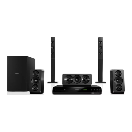
- Page 9 Your home theater Congratulations on your purchase, and support that Philips offers, register your home theater at www.philips.com/welcome. Main unit a Disc compartment b Display panel (Open/Close) Open or close the disc compartment. (Play/Pause) Start, pause or resume play. e SOURCE Select an audio or video source for the home theater.
- Page 10 AUDIO SOURCE: Select an audio Open or close the disc compartment. input source. (Home) RADIO: Switch to FM radio. Access or exit the home menu. USB: Switch to USB storage device. q AUDIO SYNC c Navigation buttons Select an audio language or channel. Navigate menus.
- Page 11 b SPEAKERS Connect to the supplied speakers and subwoofer. c VIDEO OUT Connect to the composite video input on the TV. d AUDIO IN-AUX Connect to an analog audio output on the TV or an analog device. e DIGITAL IN-OPTICAL Connect to an optical audio output on the TV or a digital device.
- Page 12 Connect and set up FRONT FRONT FRONT WOOFER LEFT RIGHT CENTER This section helps you connect your home theater to a TV and other devices, and then set it up. For information about the basic connections of your home theater and accessories, see the quick start guide.
- Page 13 SUBWOOFER (subwoofer): such as volume control for both the Place the subwoofer at least one meter TV and the home theater. (see 'Set to the left or right of the TV. Leave about up EasyLink (HDMI-CEC control)' on 10-centimeter clearance from the wall. page 10) If you cannot hear the TV audio through your home theater, set up the audio...
- Page 14 If you cannot hear the TV audio through Connect audio from TV and your home theater, set up the audio other devices manually. Play audio from TV or other devices through Note your home theater speakers. If your TV has a DVI connector, you can use an HDMI/ Use the best quality connection available on DVI adapter to connect to TV.
- Page 15 For information on your device, see Using an analog cable, connect the AUX the user manual of the device. connectors on your home theater to the Philips does not guarantee 100% interoperability with AUDIO OUT connectors on the TV or all HDMI-CEC devices. other device.
- Page 16 To play the audio from the TV EasyLink controls speakers, select [Off], and skip the following steps. With EasyLink, you can control your home theater, TV, and other connected HDMI-CEC Select [HDMI Setup] > [EasyLink Setup] compliant devices with a single remote control. >...
-
Page 17: Mechanical And Dismantling Instructions
Mechanical and Dismantling Instructions Dismantling Instruction Detailed information please refer to the model set. The following guidelines show how to dismantle the player. Step1: Open the top cover. Remove 2 screws on both sides and 4 screws on back panel,then open the cover. (Figure 1) Figure 1 Step2:Dismantle the loader.Open the tray,dismantle the CD door,remove 2 screws beside the loader. - Page 18 Mechanical and Dismantling Instructions Dismantling Instruction Detailed information please refer to the model set. The following guidelines show how to dismantle the player. Step3: Dismantle the main board.Disconnect connectors(XP221,XP82,XS751),remove 2 screws on the board and 6 screws on back panel.(Figure 3) Step4: Dismantle the power board.Remove 4 screws on the board.(Figure 3) XS751 XP221...
-
Page 19: Software Upgrades
Software Upgrade 1. There are 2 ways to software upgrade: First: Upgrade from USB: Copy the upgrade file HTD5510_X X.BIN to USB then press the USB key on RC or SOURCE key on front panel. When upgrade file detected, select "Yes" to upgrade, select "Cancel" to cancel. ... -
Page 20: Trouble Shooting Chart
5 - 1 Trouble shooting chart No display on LED, and buttons do not work No display on LED, and buttons do not work Check XP3 pin14 Check Q751 in It should be 5V main board Replace Q751 Check the front board signals VSCLK,VSDA,VSTB Check the main board SPI signal... - Page 21 5 - 2 Trouble shooting chart No audio output No audio output +34V refer < Check 34v voltage on AMP board is normal output > Check the signals of I2S (U20 Pin Replace main board 34,35,36,42,43,44) Check the I2S signals (U1500 Pin Check the PCB Layout 11,22,23,24,25,26) Check the PWM signals (U1500...
- Page 22 5 - 3 Trouble shooting chart Remote control does not work Remote control does not work Check whether the remote Replace the battery for remote controller controller’s battery exhausted or not. In the front control board,check Replace IR601 IR601 pin1 Waveform In the main board U20 Check the pcb layout pin 16 waveform...
- Page 23 Trouble shooting chart 5 - 4 Can’t read disc or can’t open the disk door Can’t read disc or can’t open the disk door Check whether Check the connection 4pin cable from the DVD loader running is main board normal Check 24pin cable from main board connection to Fix the connection the 24pin cable...
- Page 24 5 - 5 Trouble shooting chart No video display No Video display Check if R899 is on Add R188,For Indian ,add CE881 For Indian ,please check CE881 Replace the main board...
- Page 25 5 - 6 Trouble shooting chart No output by Optical in No output by Optical in Check Optical in mainboard P451 connector P451 Check U451 power supply pin5 Check system power supply Replace U451...
- Page 26 Trouble shooting chart 5 - 7 No output by Aux IN No output by Aux in Check U361 pin1 ,12 line to main board Aux In Check U211 pin1 , 2 Replace U5 Check U211 I2S output Replace U211 pin9 , 10,11,12 Replace Main board...
- Page 27 Trouble shooting chart NO +12V 、+5 and +34V output +12V output whether Check AC input Check whether Powerline is good voltage is OK. electrical contact. whether Check the voltage of Check BD501 and F501 CE501&CE502 is OK whether Check the voltage of Check D505and D503 CE511 &CE503 is between 5.5V and 6.5V.
- Page 28 Trouble shooting chart No +5V output No +5V output Check whether Check D516、D518 voltage of CE516 is +5V. whether Check U504、 U509 and Replace component T501 is OK.
- Page 29 5-10 Trouble shooting chart No +12V output No +12V output Check whether Check D515 voltage of CE512 is +12V. U504 、 whether Check Replace component U509 and T501 is OK.
- Page 30 5-11 Trouble shooting chart No +34V output No +34V output whether Check Check U507、D503、ZD509、ZD502 voltage CE503 between 5.5V and 6.5V. Check whether Check D514 voltage CE507 +34V. U503 、 whether Check U507 and T502 is OK. Replace component...
- Page 31 Block Diagram for HTD5540: HDMI CVBS TUNER OPTICAL AC IN CEN/RR RL/SW FR/FL Connector RZ5B 74CH02 TS5A 3157 74HC4052 F4558 MPEG Decode SPHE8203 AK5358 AK5358 TAS5352 TAS5352 TAS5352 TAS5352 TAS5352 TAS5352 AM5890 Main Board & AMP Board 24PIN 24PIN 6PIN 6PIN 2PIN 2PIN...
- Page 32 Front Control Board Circuit Diagram: ST5V R637 R637 VSCLK R641 R641 VSDA R639 R639 VSTB KEY_POW R704 R704 R705 R705 R694 R694 R703 R703 MP3_L 4.7K 4.7K 4.7K 4.7K 4.7K 4.7K MP3_R U301 U301 DRIVER_LED_ET6202 DRIVER_LED_ET6202 GRID[1:7] GRID1 GRID1 MIC_Detect VSDA GRID1 GRID2...
- Page 33 Power Board Circuit Diagram: CY505 CY505 470pF/250VAC 470pF/250VAC 01U0PWOPP-PW101 C507 2200pF/1KV C507 2200pF/1KV R527 R527 JP509 JP509 T502 T502 NC/Jumper NC/Jumper PQ3230 PQ3230 C506 C506 10/1W 10/1W R515 R515 +34V_1 +34V 0.0022uF(222)400V 0.0022uF(222)400V ZD508 ZD508 R516 R516 R517 R517 R518 R518 D514 SF20A300HPI/20A/300V D514 SF20A300HPI/20A/300V...
- Page 34 Main Board Circuit Diagram:Power TO POWER BOARD PVDD XP751 XP751 12 : PVDD FB1501 FB80@100MHz FB1501 FB80@100MHz 11 : PVDD 10 : PVDD FB1502 FB80@100MHz FB1502 FB80@100MHz ST5V 9 : PGND 8 : PGND P+5V 7 : PGND A+5V To Servo R751 R751 Q751...
- Page 35 Main Board Circuit Diagram:SPHE8203R TP20 TP20 DVCC3 VCC1.2 RF3.3V DAC_VREF CE20 CE20 RFGND A+5V A+5V 47uF/16V 47uF/16V XP100 XP100 A+5V CE100 CE100 RFGND FOC- C100 C100 0.1uF/25V/Y5V 0.1uF/25V/Y5V FOC+ V_FSADJ 1K/1% 1K/1% RAD+ R100 R100 NC/100uF/16V NC/100uF/16V RAD- close to XP100 VCC3.3V RFGND LDSW...
- Page 36 Main Board Circuit Diagram:Analog Video Output P+5V SCART16 R881 R881 NC/180 NC/180 VCC3.3V Q881 Q881 R/V_OUT R882 R882 NC/0 NC/0 C891 C891 R883 R883 NC/NPN_3DG3904M NC/NPN_3DG3904M TV_DAC3 NC/0.1uF/25V/Y5V NC/0.1uF/25V/Y5V NC/1K NC/1K R884 R884 R885 R885 NC/4.7K NC/4.7K C882 C882 R886 R886 NC/100pF/50V/NP0 NC/100pF/50V/NP0...
- Page 37 Main Board Circuit Diagram:Audio Input Vref Vref R399 R399 R401 R401 R409 R409 R408 R408 Q845 Q845 FB841 FB841 P+5V FM_3.3V MP3_L R362 R362 C362 1uF/16V/Y5V C362 1uF/16V/Y5V AL_CH3 NPN_MMBT8050C NPN_MMBT8050C 500/500mA 500/500mA FM_L R849 R849 8.2K 8.2K C862 C862 2.2uF/10V/Y5V 2.2uF/10V/Y5V TUNER_L...
- Page 38 Main Board Circuit Diagram:HDMI & USB Differential signal trace (TXC+/-, TX1+/-, TX2+/- and TX0+/-): 50ohm single end and 100ohm differential impedance No via & length than 5cm VCC3 VCC5 FL851 NC/ACM2012H-900-2P FL851 NC/ACM2012H-900-2P P851 P851 TXC+ TXC+ TX2+ TXC- TXC- TX0+ TX0+ C851...
- Page 39 Main Board Circuit Diagram:TAS5538 VCC3.3V AMP_3.3V FB1500 FB1500 500/500mA 500/500mA C1500 C1500 CE1500 CE1500 CE1501 CE1501 220uF/16V 220uF/16V 0.1uF/25V/Y5V 0.1uF/25V/Y5V 47uF/16V 47uF/16V +12V Q1500 Q1500 XP1500 XP1500 PNP_MMBT8550CLT1 PNP_MMBT8550CLT1 AMP_3.3V R1501 R1501 U1500 U1500 R1505 R1505 TGND + CE1502 + CE1502 C1510 C1510 C1511...
- Page 40 Main Board Circuit Diagram:AMP TAS5342*2 NOTE ALL CHANEL POWER SUPPLY NET \SPEAKER OUT NET AND ITS WIRE WIDE=3.5MM +12V R1600 R1600 C1600 C1600 R1601 R1601 C1601 C1601 C1602 C1602 0.1uF/50V/X7R 0.1uF/50V/X7R 0.1uF/50V/X7R 0.1uF/50V/X7R 0.1uF/50V/X7R 0.1uF/50V/X7R C1603 C1603 U1600 U1600 LC DEMODULATION 0.1uF/50V/X7R 0.1uF/50V/X7R PVDD...
- Page 41 7-10 7-10 Main Board Circuit Diagram:AMP TAS5352*1 R1700 R1700 +12V WIRE WIDE=3MM WIRE WIDE=1MM R1701 R1701 C1700 C1700 C1701 C1701 C1702 C1702 0.1uF/50V/X7R 0.1uF/50V/X7R 0.1uF/50V/X7R 0.1uF/50V/X7R 0.1uF/50V/X7R 0.1uF/50V/X7R C1703 C1703 0.1uF/50V/X7R 0.1uF/50V/X7R U1700 U1700 GVDD_B GVDD_A 0.033uF/50V/X7R 0.033uF/50V/X7R WIRE WIDE=3MM C1704 C1704 BST_A...
- Page 42 7-11 7-11 Front Control Board print-layout:...
- Page 43 7-12 7-12 Power Board print-layout:...
- Page 44 7-13 7-13 Main Board print-layout(bottom side):...
- Page 45 7-14 7-14 Main Board print-layout(top side):...
- Page 46 Voltages for per connect pin XP751 from main board to power board Pin No. Pin Assign Remark 1 AMP_ON/OFF AMP_ON/OFFsignal 2 +P_12V 12V 3,4,7,8,9 GND GND 5,6 M_5V 5V 10,11,12 PVDD 34V XP221 from main board to FB board PIN NO. PIN Assign Remark 1 VCC‐USB 5V 2 GND GND 3 USB_DM USB D‐ 4 USB_DP USB D+ XP82 from main board to FB board ...
- Page 47 XP136(4‐5) from main board to Loader Pin No. Pin Assign Remark 4 GND GND 5 TRAYIN TRAYIN signal XP100 from main board to Loader Pin No. Pin Assign Remark 1,9,13 GND GND 2 PUH_DVDLD PUH_DVDLD signal 3,4 NC / 5 CDMDI CDMDI signal 6 PUSH_CDLD PUSH_CDLD signal 7 DVDVR DVDVR signal 8 CDVR CDVR signal 10 E E signal 11 ...
- Page 48 SPHE8203R/Rx MAIN IC BLOCK DIAGRAM...
- Page 49 SPHE8203R/Rx SIGNAL DESCRIPTION Pin Configuration...
- Page 50 SPHE8203R/Rx Pin Description Pin Name Pin Type Description SPDC_OUT Servo SPDC OUT SC_OUT Servo SC OUT DMEA Servo DMEA DVDVR/GPIO/STEP_OUT Servo STEP OUT CDVR/GPIO/SC1_OUT Servo SC1 OUT TRAY_OUT/GPIO/DFCT Servo TRAY OUT TRAYIN/GPIO/FGIN Servo TRAYIN or I2C CLK or GPIO[9] TRAY+/GPIO/TRAYOUT Servo TRAYOUT or GPIO[10] SCART_SIG / GPIO SCART_SIG / GPIO[11]...
- Page 51 SPHE8203R/Rx Pin Name Pin Type Description HDMI_HPD/GPIO GPIO [52] [IO] HDMI_CEC/GPIO GPIO [53] [IO] DDC_SDA GPIO [54] [IO] DDC_SCL GPIO [55] [IO] AUDIO_MUTE/GPIO GPIO [56] [IO] SPDIF_IN GPIO [57] [IO] SPDIF_OUT GPIO [58] [IO] VDD12 Kernel logic power supply pins for chip kernel logic and input pre-driver #1 VDD_33 I/O power supply pins #2 V_COMP...
- Page 52 SPHE8203R/Rx Pin Name Pin Type Description TX2+ HDMI TX2+ HAPGND Ground pin for HDMI PHY AD_AVDD 3.3V power for ADC HOME/GPIO servo test out 0 or GPIO[96] (HOME) LDSW/GPIO servo test out 1 or GPIO[97] (LDSW) AD_AVSS ADC ground pin RF_AVDD 3.3V power for RF AGCCAP...
- Page 53 10-1 10-1 Exploded View for HTD5540/12/93:...
- Page 54 10-2 10-2 Exploded View for HTD5510/94 HTD5540/94 HTD5570/94...
- Page 55 10-3 10-3 Exploded View for HTD5510/98 HTD5540/98 HTD5570/98...
-
Page 56: Revision List
1 1 - 1 Revision List Version 1.0 Initial Release for HTD5540/12/98/94/93.