Panasonic EB-X70 Service Manual
Hide thumbs
Also See for EB-X70:
- Operating instructions manual (158 pages) ,
- Service manual (82 pages) ,
- Technical information (4 pages)
Table of Contents
Advertisement
Quick Links
Download this manual
See also:
Technical Information
Service Manual
This service information is designed for experienced repair technicians only and is not designed for use by the general
public. It does not contain warnings or cautions to advise non-technical individuals of potential dangers in attempting to
service a product.
Products powered by electricity should be serviced or repaired only by experienced professional technicians. Any attempt to
service or repair the product or products dealt with in this service manual by anyone else could result in serious injury or
death.
Issue 1
Revision 0
EB-X70
Tx Frequency Range:
Rx Frequency Range:
Tx / Rx separation
RF Channel Bandwidth
Number of RF channels
Speech coding
Operating temperature
Type
RF Output Power
Modulation
Connection
Voice digitizing
Transmission speed
Signal Reception
Antenna VSWR
Dimensions
(excluding
antenna)
Volume
Weight
Main Display
Sub Display
Illumination
Keys
SIM
External DC Supply
Voltage
Battery
Standby Time
Talk Time
Talk and standby time will be dependent on network conditions, SIM card, backlight usage
and network condition.
WARNING
© 2003
Development of Europe Ltd. All rights reserved.
Unauthorized copying and distribution is a violation
of law.
Order Number: PMCD030901C8
Digital Cellular Phone
900 MHz
1800 MHz
1710 -1785 MHz
880 - 915MHz
1805 -1880 MHz
925 - 960 MHz
45 MHz
95 MHz
200 kHz
174
374
Full rate/Half rate/Enhanced Full rate
-10 °C to +55 °C
Class 4 Handheld
Class 1 Handheld
2 W maximum
1 W maximum
GMSK (BT = 0.3)
8 ch / TDMA
13 kbps RPE-LTP / 13 kps ACLEP / 5.6 kps CELP / VSLEP
270.833 kbps
Direct conversion
< 2.1 : 1
Height: 87.3 mm
Width: 47.1 mm
Depth: 24 mm
80 cc
95 g
LCD, 176 x 132 pixels, 65,536 colours
LCD, 96 x 28 pixels, monochrome
10 LEDs for Keypad Backlighting (White)
4 LEDs for LCD Backlighting (White)
3 LEDs for Sub LCD (Blue, Green, Orange)
17-key Keypad, Navigation key, 1 memo key
3 V Plug-in type only
5.8 V
3.7 V nominal, 680mAh, Li-Ion
Panasonic
Mobile
1900 MHz
1850 - 1910 MHz
1910 - 1990 MHz
60 MHz
299
Class 1 Handheld
1 W maximum
Communications
Advertisement
Table of Contents

Related Manuals for Panasonic EB-X70


Summary of Contents for Panasonic EB-X70
- Page 1 Order Number: PMCD030901C8 Service Manual Digital Cellular Phone EB-X70 900 MHz 1800 MHz 1900 MHz 1710 -1785 MHz 1850 - 1910 MHz Tx Frequency Range: 880 - 915MHz 1805 -1880 MHz 1910 - 1990 MHz Rx Frequency Range: 925 - 960 MHz...
-
Page 2: Table Of Contents
Every care has been taken to ensure that the contents of this manual give an accurate representation of the equipment. However, Panasonic Mobile Communications Development of Europe Ltd. accepts no responsibility for inaccuracies which may occur and reserves the right to make changes to the specification or design without prior notice. -
Page 3: Introduction
1.1. Purpose of this Manual This Service Manual contains the information and procedures required for installing, operating and servicing the Panasonic GSM Personal Cellular Mobile Telephone system operating on GSM Digital Cellular Networks. -
Page 4: Structure Of The Manual
INTRODUCTION 1.2. Structure of the Manual The manual is structured to provide service engineering personnel with the following information and procedures: General and technical information - provides a basic understanding of the equipment, kits and options, together with detailed information for each of the major component parts. Installation and operating information - provides instructions for unpacking, installing and operating the equipment. -
Page 5: General Description
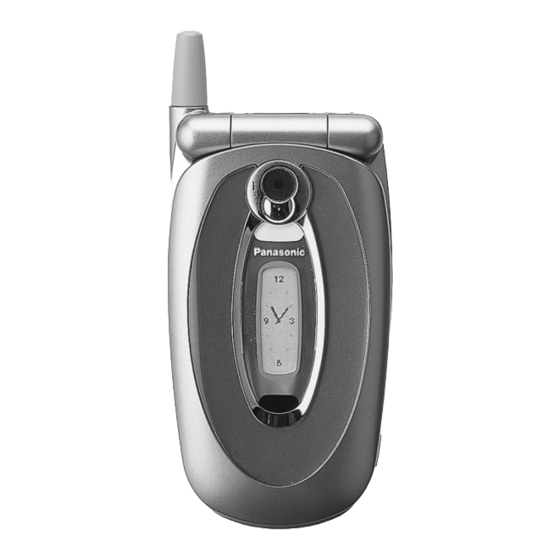
2.3. Features The Panasonic Phone Model X70 is a high performance, small, light, telephone handsets for business and domestic use on General Packet Radio Service (GPRS) running on GSM networks. The following features are provided: • Triple Band, EGSM900, GSM1800 and GSM1900 operation. -
Page 6: Operating Instructions
OPERATING INSTRUCTIONS 3 OPERATING INSTRUCTIONS 3.1. General This section provides a brief guide to the operation and facilities available on the telephone handset. Refer to the Operating Instructions supplied with the telephone for full operational information. 3.2. Controls and Indicators Earpiece Main Display Antenna... -
Page 7: Liquid Crystal Displays
OPERATINGINSTRUCTIONS 3.3. Liquid Crystal Displays The telephone handset has two Liquid Crystal displays - a colour display for main operation and a monochrome sub-display for a quick review of phone status. Figure 3.3: Main Liquid Crystal Display 3.4. Alpha Entry 3.4.1 Character Set / Key Assignments Alpha entry is used to enter alphanumeric characters in to the Phonebook, Short Messages and Greeting Message areas... -
Page 8: Features Menu Structure
OPERATING INSTRUCTIONS 3.5. Features Menu Structure 1. Settings Display Wallpaper Alerts Ring Volume On/Off Show Keys Ring Type Brightness Phone Settings Language Quiet Mode Backlight Time Clock DTMF Length Vibration Alert Key Baclight All Tones Call Service Melody Composer Create Clock/Calendar Call Divert Active Flip... -
Page 9: Imei And Software Identification
OPERATING INSTRUCTIONS 3.6. IMEI and Software Identification To check the IMEI number of the phone: Press: * # 0 6 # To identify the software version installed on the phone: Press: * # 9 9 9 9 # within five seconds of switching on. 3.7. - Page 10 OPERATING INSTRUCTIONS 3.7.5 Enabling Procedure 1. Press 2. Scroll up / down to select: "SIM" for SIM Personalisation "Network" for Network Personalisation "Sub-Network" for Sub-Network Personalisation "ServiceProvider" for Service Provider Personalisation, or "Corporate" for Company Personalisation. 3. Press 4. Enter the 8 or 16 digit Control Key and press 5.
-
Page 11: Technical Description
TECHNICAL DESCRIPTION 4 TECHNICAL DESCRIPTION 4.1. RF Overview 4.1.1 General Specifications The telephone is a triple band product incorporating three switchable transceivers, EGSM 900 band,GSM 1800 (DCS 1800) band and GSM 1900 band. The transmit and receive bands are given in the table below: EGSM 900 880-915 MHz 925-960 MHz... -
Page 12: Block Diagram
TECHNICAL DESCRIPTION 4.1.3. Block Diagram FRONT END TRIPLE BAND TRANSCEIVER BASEBAND (SWITCH MODULE) FILTERS EGSM 900 BASEBAND AMPLIFIERS GSM 1800 GSM 1900 ÷4 BUFFER AMP EGSM 900 COUPLER ÷2 TRIPLE ATTENUATORS BAND COUPLER 1800 / 1900 GSM 1800 / 1900 PA RAMP 10699-1 Figure 4.1: RF Block Diagram... -
Page 13: Transmitter
TECHNICAL DESCRIPTION 4.1.6. Antenna The antenna is a fixed helical type and is designed for triple band operation (EGSM 900, GSM 1800 and GSM 1900). 4.2. Transmitter 4.2.1 Functional Description U603 U601 ÷4 FL600 U604 FL608 TRIPLE BAND SWITCH BUFFER AMP ANTENNA ATTENUATOR MODULE... -
Page 14: Receiver
TECHNICAL DESCRIPTION 4.3. Receiver 4.3.1 Functional Description FL600 U603 SWITCH TRIPLE BAND TRANSCEIVER MODULE BASEBAND FILTERS EGSM 900 BASEBAND AMPLIFIERS GSM 1800 GSM 1900 10698-1 Figure 4.4: Receiver Block Diagram The main building block for the receiver is the transceiver IC (U605) which includes a direct conversion receiver with I and Q quadrature demodulation. -
Page 15: Baseband Overview
TECHNICAL DESCRIPTION 4.4. Baseband Overview 4.4.1 Introduction The Baseband circuits of the phone are required to perform the following functions: • Equalisation • Channel coding / decoding • Speech coding / decoding • Data Encryption • Layer 1, 2 and 3 software tasks •... - Page 16 TECHNICAL DESCRIPTION The Baseband circuits are built around a GSM chipset developed by Texas Instruments. The chipset comprises two chips, CALYPSO+ and SYREN. The highly integrated nature of the chips means that each contain a large number of functions. CALYPSO+ is a signal processing device with a digital signalling processor (DSP) and CPU. The DSP performs channel and speech encoder/decoder tasks, together with equalisation and encryption.
-
Page 17: Camera Module
TECHNICAL DESCRIPTION 4.4.3 LCD Modules The handset has two displays forming a single module. The main display is positioned inside the clamshell of the handset while the sub display is mounted on the outside of the top half of the handset. The Main LCD module consists of a Transmissive TFT colour display driven by a chip-on-glass driver connected to the LCD / Camera interface. -
Page 18: Calypso
TECHNICAL DESCRIPTION 4.4.6. Infrared Transceiver The Infrared transceiver is a 115 kbits/s IrDA transceiver with a transmission range of approximately 20 cm. The transceiver is connected directly to CALYPSO+ via RX, TX and shutdown (SD) data lines. 4.5. CALYPSO+ 4.5.1 Introduction CALYPSO+ contains the DSP, CPU, GSM timing and peripheral functions. -
Page 19: Cpu Memory
TECHNICAL DESCRIPTION 4.5.4 CPU Memory The phone uses the following memory configuration: • 256 Mbits Flash memory • 5 Mbits internal SRAM • 128 Mbits external PSRAM Although CALYPSO+ has 5 Mbits internal memory, only the external PSRAM memory is protected by the backup battery. 4.5.5 Real Time Clock (RTC) Clock functions are provided by a Real Time Clock built into CALYPSO+. -
Page 20: Syren
TECHNICAL DESCRIPTION 4.6. SYREN 4.6.1 Introduction SYREN U120 contains the interace circuits to the audio, RF and auxiliary analogue functions. It is configured using the TSP on CALYPSO+ and interfaces with the DSP in CALYPSO+ via the voice and I & Q interfaces. U120 PARAMP SYREN... -
Page 21: Bluetooth Module
TECHNICAL DESCRIPTION 4.7. Bluetooth Module Bluetooth module U500 provides short range (typically 10 metres or less) connectivity from the handset to Bluetooth-enabled devices such as headsets, car kits, personal computers for transferring voice and data. VCXO_EN VCXO 26 MHz ÷2 U120 U120 U100... -
Page 22: Power Supplies
TECHNICAL DESCRIPTION 4.8. Power Supplies 4.8.1 Introduction VBAT U120 SYREN VBACKUP U142 VBAT BACKUP VBAT CELL U141 D18V U140 VRRAM FLASH + SRAM Q202 D28V VRMEM D18VMEM D28VB VRIO1 MAIN BATTERY VRIO2 U301 U500 MELODY BLUETOOTH U100 GENERATOR BAT-TEMP VRABB CALYPSO A28BB VRDBB... -
Page 23: Voltage Regulation
TECHNICAL DESCRIPTION 4.8.3 Power On / Off Control The power on sequence can begin when VBAT >2.6 V or VBACKUP >2.6 V. In this state SYREN (U120) is in Power On Condition and internal supply UPR is active. RESPWRONZ signal to CALYPSO+ (U100) is released high. If SYREN is in the Power On Condition, one of following conditions start the Power Up sequence. - Page 24 TECHNICAL DESCRIPTION • D18VMEM / D18V: Power supply used by Flash and PSRAM memory and memory I/O, vibrate. Voltage 1.8 V ±0.1 V Current 450 mA max. Dropout 100 mV max (load max) Supply VBAT The D18V power supply is provided by a permanently enabled discrete 1.8V regulator IC. This rail is used to supply the vibrate motor and is FET switched to provide the D18MEM rail for the CALYPSO+ memory interface and external flash memory IC.
- Page 25 Over Voltage Protection As the accessory connector is unique to Panasonic, only approved chargers can be used with the handset. Therefore, no additional circuitry is required within the handset to prevent the charger voltage exceeding the design limit of 20 V.
- Page 26 TECHNICAL DESCRIPTION 4.8.8. Accessory Control The telephone can detect accessories connected to the I/O connector by measuring the ADC value of ADIN4 (ACCY_ID) on SYREN. It can then communicate with the detected peripheral and control set ACC_PWR where required, as detailed in the following table.
-
Page 27: Repair Procedures
REPAIR PROCEDURES 5 REPAIR PROCEDURES 5.1. Introduction This section describes the equipment and software required to test and calibrate the phone. Calibration Procedures are described in Section 9. The handset can be connected to a compatible personal computer for electronic adjustment and fault diagnosis. This section provides a description of the equipment required to perform those tasks. -
Page 28: Jigs And Tools
REPAIR PROCEDURES 5.4. Jigs and Tools 5.4.1 Personal Computer (PC) The PC (IBM compatible) is used as a Unit Under Test controller. This, in conjunction with the channel box software, allows all of the test facilities normally provided through the keypad of the Unit Under Test. The Microsoft Windows®... - Page 29 REPAIR PROCEDURES 5.4.4. Power Supply (2) A power supply is required to provide power to the PCB via the PCB Repair Jig while a second unit is required to provide power baseband calibration and unit testing. 5.4.5 Channel Box Software This is the test software for the telephone unit and should be installed onto the personal computer to be used for testing.
-
Page 30: Using The Channel Box Software
Check that the handset is powered-up (LCD is backlit and all LEDs are on). The Channel Box should also display handset IMEI number and Firmware version information in the left-hand column of the screen. A toolbar should also be visible in the top panel where the Panasonic logo is displayed. Figure 5.5: Channel Box Toolbar Additional user instructions are provided in the documentation files supplied with the Channel Box. -
Page 31: Disassembly / Reassembly
DISASSEMBLY / REASSEMBLY INSTRUCTIONS 6 DISASSEMBLY / REASSEMBLY INSTRUCTIONS General 6.1. This section provides disassembly and reassembly procedures for the main components of the telephone. These assemblies MUST be performed by qualified service personnel at an authorised service centre. The following Warnings and Cautions MUST be observed during all disassembly / reassembly operations: WARNING The equipment described in this manual contains polarised capacitors utilising liquid electrolyte. -
Page 32: Disassembly
DISASSEMBLY / REASSEMBLY INSTRUCTIONS 6.2. Disassembly 6.2.1. Lower case assembly and main board removal Remove the battery from the phone. 10715-1 Using tweezers, remove the four grey screw caps. Discard these items. 10716-1 Use the Trident screwdriver to remove the four case screws. Retain the screws for re-use. Remove the I/O cover and retain for reassembly. - Page 33 DISASSEMBLY / REASSEMBLY INSTRUCTIONS Undo the two screws securing the hinge strap. Retain the screws. Slide the hinge strap forwards (towards the upper case unit) to remove it, taking care not to damage the board to board flexi-strip. 10718-1 Gently twist the upper case assembly to lift the Main PCB away from the lower case back. Separate the PCB from the upper case assembly by disconnecting the ribbon cable from connector CN200.
- Page 34 DISASSEMBLY / REASSEMBLY INSTRUCTIONS Use a strip of plastic (thickness of a credit card) to separate the case halves. 10724-1 Gently lift the receiver connector at the point marked ‘A’ below. Remove the receiver and retain for reassembly. 10725-1 Lift the display module out from the case, taking care not to damage the board-to-board flexi-strip. Disconnect the main LCD flexi-strip (‘A’), the camera (‘B’) and sub-LCD (‘C’) flexi-strips.
-
Page 35: Removal Of Hinge Unit And Spigot
DISASSEMBLY / REASSEMBLY INSTRUCTIONS 6.2.3. Camera removal Unhook the camera de-sense shield / flexi-strip (‘A’) out from its retaining lug on the LCD chassis. Pull the camera out from its mounting position. 10737-1 6.2.4 Removal of hinge unit and spigot Lift the upper case front from the lower case front. -
Page 36: Antenna Removal
DISASSEMBLY / REASSEMBLY INSTRUCTIONS Push the vibrate motor assembly from underneath the holder to remove it. 10722-1 Remove the speaker wires from the cable management hooks. Apply downward pressure to the holder at point ‘A’, then gently ease out the speaker in the direction shown. 10751-1 6.2.6 Antenna Removal... -
Page 37: Reassembly
DISASSEMBLY / REASSEMBLY INSTRUCTIONS 6.2.8 Microphone removal Lift the microphone insert from its recess in the handset lower case. 10739-1 6.3. Reassembly CAUTION IF ANY OF THE RF, BLUETOOTH OR BASEBAND SHIELDS ARE REMOVED FROM THE PCB AT ANY TIME, THEY MUST BE REPLACED BY NEW ITEMS. - Page 38 DISASSEMBLY / REASSEMBLY INSTRUCTIONS Fit the display PCB by first sliding it under the sub-LCD flexi-strip and then locating over the two white posts. Locate the end of the sub-LCD flexi-strip (C) into its connector on the display PCB and lock in place. 10755-1 Refit the camera to the LCD chassis.
- Page 39 DISASSEMBLY / REASSEMBLY INSTRUCTIONS Insert the vibrate motor into the holder and secure the motor wires under the cable management hook as shown. Place the holder assembly in the location slots on the Main PCB. Connect the speaker plug into the socket marked ‘S’ on the PCB and the vibrate motor plug into the socket marked ‘V’.
- Page 40 DISASSEMBLY / REASSEMBLY INSTRUCTIONS Slide the hinge strap into position under the Main PCB. The PCB may be raised slightly to facilitate access, but take care not damage the board-to-board flexi-strip. Ensure the board-to-board connector is still firmly located over the PCB connector.
-
Page 41: Interfaces And Test Points
INTERFACES AND TEST POINTS 7 INTERFACES AND TEST POINTS 7.1. Interfaces 7.1.1 External I/O 10701-1 Figure 7.1: External I/O Connector Name HH <==>EXT Function H/H Circuit Ground 10095-2 SERIAL_UP <== Upward Serial Data (up to 812 kps Data Cable) SERIAL_DN <== Downward Serial Data (up to 812 kps Data Cable) - Page 42 INTERFACES AND TEST POINTS 7.1.2 PCB to PCB Connector CN200 10706-1 Figure 7.2: PCB to PCB Connector Bottom Connection Signal Name <==> Function Bottom Half Half 14-18 VBAT ==> Supply for Page LED, IrDA transceiver, VBAT VBAT regulators and Photo Light supply. 8, 9 ==>...
- Page 43 INTERFACES AND TEST POINTS 7.1.3 Camera Interface Connections CN901 10707-1 Figure 7.3: Camera Connector CN901 Signal Signal AVDD DATA6 AVSS DATA5 DATA4 DATA2 AVF (N/C) DATA0 DATA3 FLCK DVDD (D28VB) DATA1 DVSS (GROUND) PWDN PCLK XRESET DATA7 7.1.4. Main LCD Module Interface Connections CN902 10708-1 Figure 7.4: Main LCD Module Connector CN902...
- Page 44 INTERFACES AND TEST POINTS 7.1.5 Sub LCD Module Interface Signals CN900 10709-1 Figure 7.5: Sub LCD Module Connector CN900 Signal Signal LCD_RESET uWIRE_CS_SUB PWR_5V GND (GROUND) BLUE_CATH uWIRE_SDO GREEN_CATH uWIRE_SCLK RED_CATH VDD (D28VB) 7.1.6. IrDA Function Connection Signal PCB - IrDA D28VB DS803 IrDA Power Supply...
-
Page 45: Sim Interface
INTERFACES AND TEST POINTS 7.1.7. SIM Interface SIGNAL SIMPWR (3W) SIM_RST CN300 SIM_CLK Not connected GROUND Not connected SIM-I/O Not connected 10710-1 Figure 7.7: SIM Connection Details 7.1.8 Battery Connector GND (-ve) BAT TEMP VBAT (+ve) 10711-1 Figure 7.8: Battery Connection Details PMCD030901C8 Section 7 Issue 1... -
Page 46: Test Points
INTERFACES AND TEST POINTS 7.2. Test Points 7.2.1 Main PCB FUNCTION GRID TP100 CALYPSO+ 32kHz CLOCK TP107 D15V TP108 D28VB TP109 D28V TP110 A28V TP129 TP111 D28VR TP128 VRRTC TP112 TP113 VRSIM TP114 SYREN TDO SYREN TDI TP115 TP118 VCXO_TEMP TP119 SYREN DAC TP131... - Page 47 INTERFACES AND TEST POINTS 7.2.2 Display PCB GRID SIGNAL D28VB TP800 TP801 VBAT EXTPWR TP802 TP803 TP810 TP809 TP804 CAM_PAGE_LED TP806 CHRG_LED IRDA_SD TP808 TP809 EAR_P EAR_N TP810 TP811 IRDA_RXIR TP812 IRDA_TXIR GI/00 TP813 TP814 DS800 / R800 (P’LIGHT) DS801 / R801 (P’LIGHT) TP815 TP816 PWM0...
-
Page 48: Fault Finding
FAULT FINDING 8 FAULT FINDING 8.1. RF Waveforms NOTE: When using a FET probe, it should be protected from high power levels via a 70 dB pad. The measurements shown below are by FET probe on non-50 Ω tracks, therefore signal levels are approximate. H3 Filter O/P, single-ended measurement SMARTi O/P, single-ended measurement Stop: 1.711200 GHz... - Page 49 FAULT FINDING The output measured at the coupler (U607) output should be ~20 dB below the power amplifier output: Coupler O/P, single-ended measurement Start: 1.709200 GHz 10742-1 Stop: 1.711200 GHz Figure 8.3: GSM 1800 / GSM 1900 Coupler (U607) Signal level at the RFIN connection of the Automatic Power Controller (APC) IC (U605): APC I/P, single-ended measurement.
-
Page 50: Bga Fault Identification
FAULT FINDING 8.2. BGA Fault Identification The following process is recommended when attempting to identify a ‘no power-on’ fault or ‘intermittent power-off’ fault that could be attributed to a BGA device. START Attempt to power on the phone from the Service Channel Box. -
Page 51: Power On Fault Analysis
FAULT FINDING Fault Signal Details Suspect Device Code Serial Port Ensure connections made Check using known ‘good’ phone. correctly. Supply Voltage Vbat should be 3.7 V. Check power supply or that battery is fully charged. System Clock Check that 13 MHz is present on Check VCXO. - Page 52 FAULT FINDING Expected Power-on sequence Test Point On failure Output Supply to FLASH initialised. TP127 2.0 V DC Regulated supply to FLASH memory suspect. Code is run from FLASH memory If handset does not power on, refer to the chart below. START the phone switched-on?
-
Page 53: Calibration Procedures
CALIBRATION PROCEDURES 9 CALIBRATION PROCEDURES 9.1. Introduction NOTE: See Section 6 for a list of the equipment and setup procedures required to perform the following adjustment and calibration procedures. The following procedures MUST be performed after replacement or repair of the PCB. Failure to do so may result in incorrect operation of the telephone. - Page 54 CALIBRATION PROCEDURES 9.2.2 Power Level Tables The following tables show the measurement limits according to power level: The values in these tables are required only if manual Tx Trim is used to trim individual channels. EGSM 900 Output Power (dBm) Power Level Target (PL)
- Page 55 This procedure requires the use of a Gigatronics 8541C or Wavetek 4400 power meter. NOTE: To ensure that the telephone operates within set SAR margins, Panasonic recommends that a power meter capable of measurement to an accuracy of ±0.2 dB is used when calibrating power levels. Use of a less accurate power meter may result in the telephone failing to meet SAR standards.
-
Page 56: Rssi
CALIBRATION PROCEDURES 9. Select the ‘NEXT CAL’ button and repeat steps 7 and 8. When the message “Copy cal. values operation - click the ‘Next cal’. button”, select the ‘NEXT CAL’ button. 10. When manual calibration is complete, the new DAC values will be calculated and downloaded to the handset. The message: "Downloading new DAC values - do not remove handset”... -
Page 57: Battery Calibration
CALIBRATION PROCEDURES 9.4. Battery Calibration 9.4.1 Preliminaries There are two procedures associated with battery calibration, battery temperature and battery voltage. Connect the RF Adaptor / Baseband Jig, telephone and PC as shown in the diagram below. CABLE 1 10743-1 Figure 9.3: Battery calibration test connections Set the Interface box to POWER ON, IGN and EXT PWR OFF. -
Page 58: Camera Calibration
CALIBRATION PROCEDURES 9.5. Camera Calibration Currently there are no camera calibration procedures for this product. Issue 1 Section 9 PMCD030901C8 Revision 0 – 56 – Service Manual... -
Page 59: Replacement Parts List
REPLACEMENT PARTS LIST 10 REPLACEMENT PARTS LIST 10.1. Sub-Assemblies Ref. No. Part No. Part Name & Description MAIN BOARD - SEE SEPARATE LIST M101 1GE004CABA LOWER FRONT COVER - DARK SILVER M102 1HE003CABA LOWER BACK CASE - DARK SILVER M104 6TE002CABA KEYPAD ASSEMBLY - DARK SILVER M105... - Page 60 REPLACEMENT PARTS LIST Ref. No. Part No. Part Name & Description M154 M150 1GE002CABA UPPER FRONT COVER - DARK SILVER M151 1HE002DABA UPPER BACK CASE - DARK SILVER M153 M152 2EE004BABA MAIN LCD PANEL - DARK SILVER M153 2EE003CABA LCD PANEL SUB - DARK SILVER M154 9ZE010D MIRROR ASSEMBLY...
-
Page 61: Main Pcb Variants
CN102 X70BRD001F PCB ASSY LANGUAGE PACK F X70BRD001G PCB ASSY LANGUAGE PACK G CN600 CN602 Network-specific (SIM-locked) Assemblies M122 available - please refer to Panasonic Spares. M126 M124 10.3. Language Packs M128 M121 M125 M123 LANGUAGE PACKS LANGUAGE M127 ENGLISH ¶... - Page 62 REPLACEMENT PARTS LIST Ref. No. Part No. Part Name & Description Ref. No. Part No. Part Name & Description C152 F1H1A105A025 CAPACITOR, CER (1608) 10V 1µF C422 F1G1H470A409 CAPACITOR, CER 50V 47pF C153 F1G1A104A002 CAPACITOR, CER 10V 0.1µF C423 F1H1A105A025 CAPACITOR, CER (1608) 10V 1µF C201 F1G1A104A002...
- Page 63 REPLACEMENT PARTS LIST Ref. No. Part No. Part Name & Description Ref. No. Part No. Part Name & Description C670 ECJ0EC1H030C CAPACITOR, CER 50V 3pF FL200 J0HABB000014 EMI FILTER C671 F1G1H330A409 CAPACITOR, CER 50V 33pF FL201 J0HABB000014 EMI FILTER C673 ECJ0EC1H010C CAPACITOR, CER 50V 1pF FL202...
- Page 64 REPLACEMENT PARTS LIST Ref. No. Part No. Part Name & Description Ref. No. Part No. Part Name & Description R117 ERJ2GEJ222X RESISTOR 62.5mW 2.2k R451 ERJ2GEJ104X RESISTOR 62.5mW 100k R118 ERJ2GEJ153X RESISTOR 62.5mW 15k R457 ERJ2GEJ152X RESISTOR 62.5mW 1.5k R119 ERJ2GEJ104X RESISTOR 62.5mW 100k R458...
-
Page 65: Display Pcb
REPLACEMENT PARTS LIST Ref. No. Part No. Part Name & Description Ref. No. Part No. Part Name & Description U603 C1CB00001642 SMARTIDC+GSM TR X70 L905 ELJRF22NJFB INDUCTOR 22nH U604 C1CB00001641 GSM QUAD BAND A X70 L906 ELJRF22NJFB INDUCTOR 22nH U605 C1CB00001600 50DB GSM PA CON U607... -
Page 66: Bulk Pack Items
REPLACEMENT PARTS LIST 10.6. Bulk Pack Items Ref. Part No. Part Name & Description X70CVR01BP UPPER-LOWER COVER ASSY (200PCS) X70CAS01BP UPPER-LOWER CASE ASSEMBLY (200) AN80027AABAB ANTENNA, DARK SILVER (200PCS) 6TE002CACABP KEYPAD MEMBRANE (200PCS) 2EE003BAAABP SUB-PANEL (200PCS) 2EE004BAAABP MAIN LCD PANEL (200PCS) 6RE003BABABP SCREW CAP UPPER, DRK SILVER (500) 6RE004CABABP... -
Page 67: Circuit Diagrams
CIRCUIT DIAGRAMS 11 CIRCUIT DIAGRAMS Figure 11.1: Circuit Diagram - Baseband (Sheet 1 of 2) PMCD030901C8 Section 11 Issue 1 Service Manual – 65 – Revision 0... - Page 68 CIRCUIT DIAGRAMS Figure 11.2: Circuit Diagram - Baseband (Sheet 2 of 2) Issue 1 Section 11 PMCD030901C8 Revision 0 – 66 – Service Manual...
- Page 69 CIRCUIT DIAGRAMS Figure 11.3: Circuit Diagram - Peripherals 1 PMCD030901C8 Section 11 Issue 1 Service Manual – 67 – Revision 0...
- Page 70 CIRCUIT DIAGRAMS Figure 11.4: Circuit Diagram - Peripherals 2 Issue 1 Section 11 PMCD030901C8 Revision 0 – 68 – Service Manual...
- Page 73 CIRCUIT DIAGRAMS Figure 11.7: Circuit Diagram - RF PMCD030901C8 Section 11 Issue 1 Service Manual – 71 – Revision 0...
- Page 74 CIRCUIT DIAGRAMS Figure 11.8: Circuit Diagram - Display Module (Sheet 1 of 2) Issue 1 Section 11 PMCD030901C8 Revision 0 – 72 – Service Manual...
- Page 75 CIRCUIT DIAGRAMS Figure 11.9: Circuit Diagram - Display Module (Sheet 2 of 2) PMCD030901C8 Section 11 Issue 1 Service Manual – 73 – Revision 0...
-
Page 76: Layout Diagrams
LAYOUT DIAGRAMS 12 LAYOUT DIAGRAMS Figure 12.1: Main PCB Layout - Side A Issue 1 Section 12 PMCD030901C8 Revision 0 – 74 – Service Manual... -
Page 77: Service Manual
LAYOUT DIAGRAMS Figure 12.2: Main PCB Layout - Side B PMCD030901C8 Section 12 Issue 1 Service Manual – 75 – Revision 0... - Page 78 LAYOUT DIAGRAMS Figure 12.3: Display PCB Layout - Side A Issue 1 Section 12 PMCD030901C8 Revision 0 – 76 – Service Manual...
- Page 79 LAYOUT DIAGRAMS Figure 12.4: Display PCB Layout - Side B PMCD030901C8 Section 12 Issue 1 Service Manual – 77 – Revision 0...
- Page 80 LAYOUT DIAGRAMS Issue 1 Section 12 PMCD030901C8 Revision 0 – 78 – Service Manual...
- Page 82 PMCDE UK030902000PJ...