Table of Contents
Advertisement
Quick Links
SERVICE MANUAL
Ver. 1.1 2006. 02
Recording media
Built-in flash memory 64 MB,
Monaural recording
Recording time
HQ:
7 hours 20 minutes
SP:
19 hours 35 minutes
LP:
32 hours 10 minutes
Frequency range
HQ:
260 Hz – 6,800 Hz
SP/LP: 220 Hz – 3,400 Hz
Speaker
approx. 2.8 cm (1
Power output
250 mW
Input/Output
• Earphone jack (minijack) for
8 – 300 ohms ear receiver/headphones
• Microphone jack (minijack, monaural)
Plug in power
Minimum input level 0.6 mV
3 kilohms or lower impedance microphone
• USB connector
Power requirements
Two LR03 (size AAA) alkaline batteries:
3 V DC
Dimensions (w/h/d) (not incl. projecting parts and controls)
34.6 × 109.5 × 18.0 mm (1
Mass (incl. batteries) 68g (2.4 oz)
Sony Corporation
9-879-994-02
Connect Business Division
2006B04-1
Published by Sony Techno Create Corporation
© 2006. 02
SPECIFICATIONS
in.) dia.
1/8
× 4
×
in.)
3/8
3/8
23/32
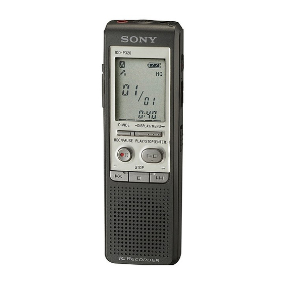
ICD-P320
Supplied accessories Operating instructions (for the IC recorder (1)/for
the application software (1))
LR03 (size AAA) alkaline batteries (2)
(US, CND model)
Headphone (1) (E, CH, KR model)
Carrying pouch (1) (E, CH, KR model)
USB connecting cable (1)
Application software (CD-ROM) (1)
Design and specifications are subject to change without
notice.
• Abbreviation
CND: Canadian model
CH : Chinese model
KR : Korean model
US Model
Canadian Model
AEP Model
UK Model
E Model
Chinese Model
IC RECORDER
Advertisement
Table of Contents

Related Manuals for Sony ICD-P320


Summary of Contents for Sony ICD-P320
- Page 1 Dimensions (w/h/d) (not incl. projecting parts and controls) 34.6 × 109.5 × 18.0 mm (1 × 4 × in.) 23/32 Mass (incl. batteries) 68g (2.4 oz) IC RECORDER Sony Corporation 9-879-994-02 Connect Business Division 2006B04-1 Published by Sony Techno Create Corporation © 2006. 02...
-
Page 2: Table Of Contents
ICD-P320 TABLE OF CONTENTS Flexible Circuit Board Repairing • Keep the temperature of the soldering iron around 270 °C during repairing. GENERAL ..............3 • Do not touch the soldering iron on the same conductor of the circuit board (within 3 times). -
Page 3: General
ICD-P320 SECTION 1 GENERAL This section is extracted from instruction manual. Index to Parts and Controls Main unit MIC (built-in microphone) i (earphone) jack (microphone) jack OPR (operation) indicator Display window ERASE DISPLAY/MENU VOL (volume) control* DIVIDE xSTOP HOLD zXREC (record) /PAUSE NxPLAY/STOP (ENTER)** –... -
Page 4: Disassembly
ICD-P320 SECTION 2 DISASSEMBLY Note : Disassemble the unit in the order as shown below. 2-1. CASE (FRONT) ASSY (Page 4) 2-2. MAIN BOARD (Page 5) 2-3. USB BOARD (Page 5) Note : Follow the disassembly procedure in the numerical order given. -
Page 5: Main Board
ICD-P320 2-2. MAIN BOARD 2 screw 1 insulating sheet 5 MAIN board CN2001 S701 2-3. USB BOARD 1 two screws 2 USB board... -
Page 6: Test Mode
ICD-P320 SECTION 3 TEST MODE 1. Outline of the TEST MODE 5-3. BEEP Test To enter the BEEP Test, press the [ERASE] button. The TEST MODE is designed to help verify the set when servicing The TEST MODE is only menu driven to select modes for servicing. - Page 7 ICD-P320 • SUSPEND Test With the VBUS ON, turn the [HOLD] switch ON to enter the HOLD SUSPEND mode. When this mode is cancelled, the VBUS is turned OFF. with VBUS Sensitivity H Nx PLAY/STOP (ENTER) HOLD x STOP HOLD...
- Page 8 ICD-P320 • Switches and corresponding LCD indications Switch Indication DIVIDE DISPLAY/MENU zX REC/PAUSE Nx PLAY/STOP(ENTER) . – Press DIVIDE button. x STOP > + ERASE HOLD-OFF Indication after DIVIDE HOLD-ON button is pressed. ERASE Indication after DISPLAY/MENU button is pressed.
-
Page 9: Diagrams
ICD-P320 SECTION 4 DIAGRAMS 4-1. BLOCK DIAGRAM MIC101 MICROPHONE A/D,D/A CONVERTER,DSP IC101 J101 Q106 SPEAKER AMP IC102 47 MIP HSSPOOT SP101 RV101 (PLUG IN POWER) –IN SPEAKER – 23 EGPIO11 XDSPIFRW EGPIO12 BIAS SCK1 EGPIO13 EGPIO14 MUTE XDSPIFACK XOUT EGPIO15... - Page 10 ICD-P320 • Waverforms THIS NOTE IS COMMON FOR PRINTED WIRING BOARDS AND SCHEMATIC DIAGRAMS. – MAIN board – (In addition to this, the necessary note is printed in each block.) IC101 ta (XOUT) Common Note on Schematic Diagrams: • All capacitors are in µF unless otherwise noted. (p: pF) 50 WV or less are not indicated except for electrolytics and tantalums.
-
Page 11: Printed Wiring Board - Main Section
ICD-P320 4-2. PRINTED WIRING BOARD — MAIN SECTION — • Refer to page 10 for Semiconductor Location. : Uses unleaded solder. MIC101 MAIN BOARD (SIDE A) MICROPHONE D2008 W102 R102 W502 S705 CN701 . – S707 TP103 TP701 X2001 TP505... -
Page 12: Schematic Diagram - Main Section (1/2)
ICD-P320 • Refer to page 10 for Waveform. 4-3. SCHEMATIC DIAGRAM — MAIN BOARD (1/2) — • Refer to page 16 for IC Block Diagrams. R137 RV101 C127 R124 R128 Q101 R126 C124 R2021 C2008 R135 C132 IC B/D C122... -
Page 13: Schematic Diagram - Main Section (2/2)
ICD-P320 • Refer to page 10 for Waveforms. 4-4. SCHEMATIC DIAGRAM — MAIN BOARD (2/2) — • Refer to page 17 for IC Pin Description. (Page 12) IC2001 TP2001 C2003 R727 R726 R728 IC701 R712 R711 D702 D701 R713 IC703... -
Page 14: Printed Wiring Board - Usb Section
ICD-P320 4-5. PRINTED WIRING BOARD — USB SECTION — : Uses unleaded solder. USB BOARD (SIDE A) USB BOARD (SIDE B) (Page 11) MAIN BOARD CN2001 W1001 CN1002 TP1001 R1019 R1010 1-869-170- (11) 1-869-170- (11) CN1001 (USB) ICD-P320... -
Page 15: Schematic Diagram - Usb Section
ICD-P320 4-6. SCHEMATIC DIAGRAM — USB SECTION — CN1002 (Page 12) R1010 CN1001 C1008 R1003 R1030 R1031 R1004 R1011 R1019 TP1001... - Page 16 ICD-P320 • IC Block Diagrams IC102 MM3111AWLE (MAIN Board (1/2)) IC2002 MM3111AWLE (MAIN Board (1/2)) SHUTDOWN BIAS BYPASS IC506 XC9105D091MR (MAIN Board (1/2)) BUFFER DRIVER PHASE COMPARATOR RAMP WAVE GENERATOR, PHASE COMPENSATION PWM/PFM CONTROLER ERROR CURRENT RIPPLE DETED AND FB...
- Page 17 ICD-P320 • IC Pin Description IC703 MN101C93KSB (SYSTEM CONTROL, USB/LED/LCD DRIVER) (MAIN BOARD (2/2)) Pin No. Pin Name Pin Description 1 to 4 COM0 to 3 LCD common 0 to 3 signal output 5 to 7 VLC3 to 1 LCD VLC 3 to 1 signal input Not used.
- Page 18 ICD-P320 Pin No. Pin Name Pin Description FLMCLE Flash memory command latch enable signal output FLMALE Flash memory address latch enable signal output XFLMWE Flash memory write enable clock signal output XFLMRE Flash memory read enable clock signal output 61 to 68...
-
Page 19: Exploded Views
ICD-P320 SECTION 5 EXPLODED VIEWS NOTE: • -XX and -X mean standardized parts, so • The mechanical parts with no reference they may have some difference from the number in the exploded views are not supplied. original one. • Items marked “*” are not stocked since they are seldom required for routine service. -
Page 20: Case (Rear) Section
ICD-P320 Ver. 1.1 5-2. CASE (REAR) SECTION LCD701 MIC101 Ref. No. Part No. Description Remark Ref. No. Part No. Description Remark 2-633-874-01 BUTTON (SIDE) 3-251-410-02 SHEET, INSULATING 2-633-876-01 TERMINAL (+.–), BATTERY 2-661-298-01 SPACER (LCD-P) 2-633-870-01 KNOB (HOLD) 2-633-872-01 HOLDER (LCD) -
Page 21: Electrical Parts List
ICD-P320 Ver. 1.1 SECTION 6 MAIN ELECTRICAL PARTS LIST NOTE: • Due to standardization, replacements in • RESISTORS When indicating parts by reference the parts list may be different from the All resistors are in ohms. number, please include the board. - Page 22 ICD-P320 MAIN Ref. No. Part No. Description Remark Ref. No. Part No. Description Remark IC501 6-708-467-01 IC XC6213B312NR R137 1-218-990-81 SHORT CHIP IC502 6-708-467-01 IC XC6213B312NR R138 1-218-937-11 RES-CHIP 1/16W IC503 6-708-472-01 IC XC6215B312NR R503 1-218-973-11 RES-CHIP 1/16W IC504 6-708-440-01 IC XC61CN1202NR...
- Page 23 ICD-P320 Ver. 1.1 MAIN Ref. No. Part No. Description Remark Ref. No. Part No. Description Remark R2014 1-218-953-11 RES-CHIP 1/16W ACCESSORIES R2015 1-218-990-81 SHORT CHIP ************ R2019 1-218-969-11 RES-CHIP 1/16W R2020 1-218-977-11 RES-CHIP 100K 1/16W 1-829-882-12 CORD, CONNECTION (USB) R2021...
- Page 24 ICD-P320 REVISION HISTORY Clicking the version allows you to jump to the revised page. Also, clicking the version at the upper on the revised page allows you to jump to the next revised page. Ver. Date Description of Revision 2005. 12 2006.