
Related Manuals for Clevo W255BU


Summary of Contents for Clevo W255BU
- Page 1 W255BU/W258BUQ-C/W258BUQ/W252BUM/W255BU/W251BUQ/W251BUQC/W258BWQ/W258BWQ-C/W251BWQ-C/W251BWQ/W255BW...
-
Page 3: Notebook Computer
Preface Notebook Computer W255BU/W258BUQ-C/W258BUQ/W252BUM/W255BU/W251BUQ/W251BUQC/W258BWQ/W258BWQ- C/W251BWQ-C/W251BWQ/W255BW Service Manual... - Page 4 Preface Notice The company reserves the right to revise this publication or to change its contents without notice. Information contained herein is for reference only and does not constitute a commitment on the part of the manufacturer or any subsequent ven- dor.
- Page 5 This manual is intended for service personnel who have completed sufficient training to undertake the maintenance and inspection of personal computers. It is organized to allow you to look up basic information for servicing and/or upgrading components of the W255BU/ W258BUQ-C/W258BUQ/W252BUM/W255BUC/W251BUQP/W251BUQC/W258BWQ/W258BWQ-C/W251BWQ- C/W251BWQ/W255BW series notebook PC.
- Page 6 Preface IMPORTANT SAFETY INSTRUCTIONS Follow basic safety precautions, including those listed below, to reduce the risk of fire, electric shock and injury to per- sons when using any electrical equipment: 1. Do not use this product near water, for example near a bath tub, wash bowl, kitchen sink or laundry tub, in a wet basement or near a swimming pool.
-
Page 7: Instructions For Care And Operation
Preface Instructions for Care and Operation The notebook computer is quite rugged, but it can be damaged. To prevent this, follow these suggestions: Don’t drop it, or expose it to shock. If the computer falls, the case and the components could be damaged. Do not expose the computer Do not place it on an unstable Do not place anything heavy... -
Page 8: Power Safety
Preface Avoid interference. Keep the computer away from high capacity transformers, electric motors, and other strong mag- netic fields. These can hinder proper performance and damage your data. Take care when using peripheral devices. Use only approved brands of Unplug the power cord before peripherals. -
Page 9: Battery Precautions
Preface Battery Precautions • Only use batteries designed for this computer. The wrong battery type may explode, leak or damage the computer. • Do not continue to use a battery that has been dropped, or that appears damaged (e.g. bent or twisted) in any way. Even if the computer continues to work with a damaged battery in place, it may cause circuit damage, which may possibly result in fire. -
Page 10: Related Documents
Preface Related Documents You may also need to consult the following manual for additional information: User’s Manual on CD This describes the notebook PC’s features and the procedures for operating the computer and its ROM-based setup pro- gram. It also describes the installation and operation of the utility programs provided with the notebook PC. System Startup 1. -
Page 11: Table Of Contents
Preface Contents System Startup ................1-VIII Top (W245BUQ) ................A-4 Introduction ..........1-1 Top (W240BUQ, W241BU-C, W240BW) ........A-5 Bottom (W240BU, W241BU) W/O USIM ........A-6 Overview ..................1-1 Bottom (W240BU, W241BU) With USIM ........A-7 Models Differences .................1-1 Bottom (W248BUQ, W249BU-C) ..........A-8 Specifications ..................1-2 Bottom (W240BW) WITH USIM .......... - Page 12 Preface HUDSON PCIE/ PCI/ CLOCK/ FCH .......... B-16 HUDSON GPIO/ USB/ STRAP ..........B-17 HUDSON SATA/ DEBUG IO/ SPI ..........B-18 HUDSON POWER DECOUPLING ..........B-19 POWERGOOD/ TPM ..............B-20 LVDS, INVERTER ..............B-21 HDMI/ CRT ................. B-22 CCD/ 3G ..................B-23 Card Reader/ LAN JMC261C ............
-
Page 13: Introduction
Introduction Chapter 1: Introduction Overview This manual covers the information you need to service or upgrade the W255BU/W258BUQ-C/W258BUQ/W252BUM/ W255BU/W251BUQ/W251BUQC/W258BWQ/W258BWQ-C/W251BWQ-C/W251BWQ/W255BW series notebook computer. Information about operating the computer (e.g. getting started, and the Setup utility) is in the User’s Manual. Information about drivers (e.g. VGA & audio) is also found in User’s Manual. That manual is shipped with the computer. -
Page 14: Specifications
Introduction Specifications Processor Options Memory AMD-C Series Accelerated Processing Unit - C-30 1C One 204 Pin SO-DIMM Socket Supporting DDR3 1066/ (1.2GHz) 1333MHz Memory 512KB L2 Cache, 40nm, DDR3-1066MHz, TDP 9W Memory Expandable up to 4GB AMD-C Series (Dual-Core) Accelerated Processing Unit - Card Reader C-50 2C (1.0GHz) Latest Specification Information... - Page 15 Introduction Keyboard Power Full-size “WinKey” keyboard (with numeric keypad) (for C-30, C-50, C-60 APU only) 3 Cell Smart Lithium-Ion Battery Pack, 24.42WH Communication (Factory Option) 6 Cell Smart Lithium-Ion Battery Pack, 48.84WH Built-In 10Mb/100Mb Ethernet LAN (Factory Option) 300K/1.3M Pixel USB PC Camera Module Full Range AC/DC Adapter (Factory Option) 3.75G/HSPA Mini-Card Module AC Input: 100 - 240V, 50 - 60Hz...
-
Page 16: External Locator - Top View With Lcd Panel Open
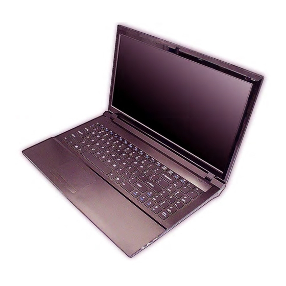
Introduction External Locator - Top View with LCD Panel Open Figure 1 Top View 1. Optional Built-In PC Camera 2. LCD 3. Power Button 4. LED Status Indicators 5. Keyboard 6. Built-In Microphone 7. Touchpad & Buttons 15.6” (39.62cm) 1 - 4 External Locator - Top View with LCD Panel Open... -
Page 17: External Locator - Front & Right Side Views
Introduction External Locator - Front & Right side Views Figure 2 Front Views 1. LED Power Indicators Figure 3 Right Side Views 1. Microphone-In Jack 2. Headphone-Out Jack 3. USB 2.0 Port 4. Optical Device Drive Bay 5. Security Lock Slot 6. -
Page 18: External Locator - Left Side & Rear View
Introduction External Locator - Left Side & Rear View Figure 4 Left Side View 1. DC-In Jack 2. External Monitor Port 3. RJ-45 LAN Jack 4. HDMI-Out Port 5. 2 * USB 2.0 Ports 6. Vent 7. Multi-in-1 Card Reader Figure 5 Rear View 1. -
Page 19: External Locator - Bottom View
Introduction External Locator - Bottom View Figure 6 Bottom View 1. Battery 2. Component Bay Cover 3. Vent/Fan Intake/ Outlet 4. Hard Disk Bay Cover 5. 3.75G/HSPA USIM Card Cover (optional) 6. Speakers Overheating To prevent your com- puter from overheating make sure nothing... -
Page 20: Mainboard Overview - Top (Key Parts)
Introduction Mainboard Overview - Top (Key Parts) Figure 7 Mainboard Top Key Parts 1. JMC261 2. ITE 8518E 3. AZALIA Codec 1 - 8 Mainboard Overview - Top (Key Parts) -
Page 21: Mainboard Overview - Bottom (Key Parts)
Introduction Mainboard Overview - Bottom (Key Parts) Figure 8 Mainboard Bottom Key Parts 1. Memory Slots DDR3 SO-DIMM 2. Accelerated Processing Unit 3. AMD Hudson M1 4. Mini-Card Connector (3G Module) 5. SIMLOCK 6. Mini-Card Connector (WLAN Module) 7. CMOS Battery 8. -
Page 22: Mainboard Overview - Top (Connectors)
Introduction Mainboard Overview - Top (Connectors) Figure 9 Mainboard Top Connectors 1. HDMI-Out Port 2. USB Port 2.0 3. Speaker Cable Connector 4. Microphone Cable Connector 5. Audio Board Connector 6. TouchPad Cable Connector 2 7. TouchPad Cable Connector 1 8. -
Page 23: Mainboard Overview - Bottom (Connectors)
Introduction Mainboard Overview - Bottom (Connectors) Figure 10 Mainboard Bottom Connectors 1. Battery Connector 2. ODD Connector 3. HDD Connector 4. CPU Fan Cable Connector 5. RJ-45 LAN Jack 6. External Monitor Port 7. DC-In Jack 8. CCD Cable Connector 9. - Page 24 Introduction 1 - 12...
-
Page 25: Disassembly
Disassembly Chapter 2: Disassembly Overview This chapter provides step-by-step instructions for disassembling the W255BU/W258BUQ-C/W258BUQ/W252BUM/ W255BU/W251BUQ/W251BUQC/W258BWQ/W258BWQ-C/W251BWQ-C/W251BWQ/W255BW series notebook’s parts and subsystems. When it comes to reassembly, reverse the procedures (unless otherwise indicated). We suggest you completely review any procedure before you take the computer apart. -
Page 26: Maintenance Tools
Disassembly NOTE: All disassembly procedures assume that the system is turned OFF, and disconnected from any power supply (the battery is removed too). Maintenance Tools The following tools are recommended when working on the notebook PC: • M3 Philips-head screwdriver •... -
Page 27: Maintenance Precautions
Disassembly Maintenance Precautions The following precautions are a reminder. To avoid personal injury or damage to the computer while performing a re- moval and/or replacement job, take the following precautions: Power Safety Warning 1. Don't drop it. Perform your repairs and/or upgrades on a stable surface. If the computer falls, the case and other Before you undertake components could be damaged. -
Page 28: Disassembly Steps
Disassembly Disassembly Steps The following table lists the disassembly steps, and on which page to find the related information. PLEASE PERFORM THE DISASSEMBLY STEPS IN THE ORDER INDICATED. To remove the Battery: To remove the Keyboard: 1. Remove the battery page 2 - 5 1. -
Page 29: Removing The Battery
Disassembly Removing the Battery Figure 1 Battery Removal 1. Turn the computer off, and turn it over. 2. Slide the latch in the direction of the arrow (Figure 1a a. Slide the latch and hold it 3. Slide the latch in the direction of the arrow, and hold it in place (Figure 1a in place. -
Page 30: Removing The Hard Disk Drive
Disassembly Removing the Hard Disk Drive The hard disk drive can be taken out to accommodate other 2.5" serial (SATA) hard disk drives with a height of 9.5mm Figure 2 (h). Follow your operating system’s installation instructions, and install all necessary drivers and utilities (as outlined in HDD Assembly Chapter 4 of the User’s Manual) when setting up a new hard disk. - Page 31 Disassembly 3. Remove the hard disk bay cover (Figure 3b Figure 3 4. Grip the tab and slide the hard disk in the direction of arrow (Figure 3c HDD Assembly 5. Lift the hard disk assembly out of the bay (Figure 3d Removal (cont’d.) 6.
-
Page 32: Removing The Optical (Cd/Dvd) Device
Disassembly Removing the Optical (CD/DVD) Device Figure 4 Optical Device 1. Turn off the computer, remove the battery (page 2 - 5) and hard disk (page 2 - Removal 2. Remove the screw at point (Figure 4a 3. Use a screwdriver to carefully push out the optical device at point (Figure 4b a. -
Page 33: Removing The System Memory (Ram)
Disassembly Removing the System Memory (RAM) Figure 5 RAM Module The computer has one memory socket for 200 pin Small Outline Dual In-line Memory Modules (SO-DIMM) supporting Removal DDR3 1333/ 1066MHz. The main memory can be expanded up to 4GB. The SO-DIMM modules supported are 1GB, 2GB and 4GB and DDRIII Modules. -
Page 34: Removing The Wireless Lan Module
Disassembly Removing the Wireless LAN Module Figure 6 Wireless LAN 1. Turn off the computer, remove the battery (page 2 - 5) and the component bay cover (page 2 - Module Removal 2. The Wireless LAN module will be visible at point on the mainboard. -
Page 35: Removing The 3.75G Module
Disassembly Removing the 3.75G Module Figure 7 3.75G Module 1. Turn off the computer, remove the battery (page 2 - 5) and the component bay cover (page 2 - Removal 2. The 3.75G module will be visible at point on the mainboard. 3. -
Page 36: Removing The Keyboard
Disassembly Removing the Keyboard Figure 8 Keyboard Removal 1. Turn off the computer, and remove the battery (page 2 - a. Remove screws from the 2. Remove screws from the bottom of the computer. Press at points to unsnap the LED cover module bottom of the computer. -
Page 37: Part Lists
Part Lists Appendix A: Part Lists This appendix breaks down the W255BU/W258BUQ-C/W258BUQ/W252BUM/W255BU/W251BUQ/W251BUQC/ W258BWQ/W258BWQ-C/W251BWQ-C/W251BWQ/W255BW series notebook’s construction into a series of illustra- tions. The component part numbers are indicated in the tables opposite the drawings. Note: This section indicates the manufacturer’s part numbers. Your organization may use a different system, so be sure to cross-check any relevant documentation. -
Page 38: Part List Illustration Location
The following table indicates where to find the appropriate part list illustration. Table A- 1 Part List Illustration Location Parts W251BUQ W251BWQ W255BU W258BUQ W258BWQ page A - 3 page A - 4 page A - 5 page A - 6... - Page 39 Part Lists Top (W251BUQ) Figure A - 1 Top (W251BUQ) 非耐落 灰色 Top (W251BUQ) A - 3...
- Page 40 Part Lists Top (W251BWQ) Figure A - 2 Top (W251BWQ) 非 耐 落 灰 色 A - 4 Top (W251BWQ)
- Page 41 Part Lists Top (W255BU) Figure A - 3 Top (W255BU) 非耐落 灰色 Top (W255BU) A - 5...
- Page 42 Part Lists Top (W258BUQ, W258BWQ) Figure A - 4 Top (W258BUQ, W258BWQ) 非耐落 灰色 A - 6 Top (W258BUQ, W258BWQ)
- Page 43 Part Lists Bottom (W251BUQ, W255BU, W258BUQ) Figure A - 5 Bottom (W251BUQ, W255BU, W258BUQ) Bottom (W251BUQ, W255BU, W258BUQ) A - 7...
- Page 44 Part Lists Bottom (W251BWQ, W258BWQ) Figure A - 6 Bot- tom(W251BWQ, W258BWQ) A - 8 Bottom (W251BWQ, W258BWQ)
-
Page 45: Lcd (W240Bu, W241Bu, W240Bw
Part Lists 頭厚 非耐落 Figure A - 7 LCD A - 9... -
Page 46: Dvd Dual
Part Lists DVD DUAL Figure A - 8 DVD DUAL 非耐落 志精 A - 10 DVD DUAL... - Page 47 Part Lists SATA-DVD (W258BWQ) Figure A - 9 SATA-DVD (W258BWQ) 非耐落 志精 SATA-DVD (W258BWQ) A - 11...
- Page 48 Part Lists DUMMY ODD Figure A - 10 DUMMY ODD 非耐落 志精 A - 12 DUMMY ODD...
- Page 49 Schematic Diagrams Appendix B: Schematic Diagrams This appendix has circuit diagrams of the W255BU/W258BUQ-C/W258BUQ/W252BUM/W255BU/W251BUQ/ W251BUQC/W258BWQ/W258BWQ-C/W251BWQ-C/W251BWQ/W255BW notebook’s PCB’s. The following table indicates where to find the appropriate schematic diagram. Table B - 1 Diagram - Page Diagram - Page Diagram - Page...
-
Page 50: Hdd
Schematic Diagrams System Block Diagram W240BU/W250BUQ/W250BAQ System Block Diagram CLICK BOARD VDD3,VDD5 6-71-W2402-D01 POWER SWITCH BOARD GPU POWER, VDDC AMD FUSION APU POWER SWITCH+HOTKEY X 3 A T I RO BS O N MVDDQ,1.8V_REG,1.0V_REG Ontario FT1 6-71-E51QS-D02 (S3 TYPE) PCIE*4 5V,3V,5VS,3.3VS 512MB DDR3 41 3-B A LL... -
Page 51: Ontario Mem & Pcie I/F, Ap
Schematic Diagrams ONTARIO MEM & PCIE I/F, AP ONTARIO MEM & PCIE I/F, AP 5 , 6 M E M_ A D D R [ 1 5 : 0 ] M E M _D A T A [ 6 3 : 0 ] 5 , 6 U 1 E M EM _ A DD R0 B 14... -
Page 52: Ontatio Display/ Clk/ Misc
Schematic Diagrams ONTATIO DISPLAY/ CLK/ MISC ONTARIO DISPLAY/CLK/MISC 1 . 8 V S R 11 1 K _ 0 4 C P U _ S V C C P U _ S V D R 12 1 K _ 0 4 R 14 3 0 0_ 1 % _ 0 4 A P U _ P W R G D... -
Page 53: Ontario Power & Decoupling
Schematic Diagrams ONTARIO POWER & DECOUPLING ONTARIO POWER & DECOUPLING 1 . 8 V S V D D C R _C P U U 1C C 2 9 C 3 1 U 1 D C 3 0 C 26 C 2 7 C 28 N 1 3 V D D C R _C PU _1... -
Page 54: Inagua Ddr3 So-Dimms A
Schematic Diagrams INAGUA DDR3 SO-DIMMS A SO -D IMM A INAGUA DDR3 SO-DIMMS A M E M _A DD R[15:0] M E M _D AT A[63:0] 2,6 JDIM M 1A M E M _ AD DR0 M E M _D AT A 0 D Q0 M E M _ AD DR1 M E M _D AT A 1... -
Page 55: Inagua Ddr3 So-Dimms B
Schematic Diagrams INAGUA DDR3 SO-DIMMS B S O-D IMM B INA GUA DDR3 S O-DIMMS B M E M _A DD R[15:0] M EM _DA T A[63 : 0] 2,5 JD IM M 2A M E M _A DDR 0 M EM _DA T A 0 M E M _A DDR 1 M EM _DA T A 1... -
Page 56: Robson S3 Pcie/ Lvds 1/6
Schematic Diagrams Robson S3 PCIE/ LVDS 1/6 Sheet 7 of 41 Robson S3 PCIE/ LVDS 1/6 B - 8 Robson S3 PCIE/ LVDS 1/6... -
Page 57: Robson S3 Main 2/6
Schematic Diagrams Robson S3 MAIN 2/6 COMPONENTS SH OWN AR E EXAMPLES ONLY AND NOT NEC ESSAR ILY QUALIFIED VBIOS FLA SH ROM U 4 B 3. 3V S _GP U 0. 1"~ 0.5 " R 10 1 A F2 TMD S _T XC P 21 5 12Kbit TX C A P_ D PA 3 P... -
Page 58: Robson S3 Mem Interface 3/6
Schematic Diagrams Robson S3 MEM Interface 3/6 COMPONENTS SHOWN ARE EXAMPLES ONLY DDR3 Memory AND NOT NECESSARILY QUALIFIED Interface DQA0_[ 31. .0] M AA[12 ..0] 1 3,14 G DDR 5/DD R3 GDD R5/D DR3 DQA0_ 0 K 2 7 MAA0 DQ A 0 _0/D QA _ 0 MAA 0 _0/ MAA _ 0 J2 9... -
Page 59: Robson S3 Straps 4/6
Schematic Diagrams Robson S3 Straps 4/6 GPIO21 MUST BE LOW DURING PERSTB WHEN BEING USED TO CONTROL MVDDQ 3.3V S _GP U P IN S T RAP S W250B AQ RE COM M E ND ED S E T T ING S R1 30 *1 0K_0 4 GP IO0... -
Page 60: Robson S3 Power 5/6
Schematic Diagrams Robson S3 Power 5/6 A A 27 PC IE_V S S #1 G ND#1 A B 24 A 30 A B 32 PC IE_V S S #2 G ND#2 A A1 3 A C24 PC IE_V S S #3 G ND#3 A A1 6 PC IE_V S S #4... - Page 61 Schematic Diagrams Robson S3 Power 6/6 M V D DQ 2.8A 21 0m il MV D D Q *0 . 1u _ 10 V _X 5R _ 0 4 *0 . 1 u_ 10 V _X 5 R _0 4 * 1u _6 .
-
Page 62: Robson Ddr3 Mem Ch-A
Schematic Diagrams Robson DDR3 MEM CH-A COMPONENTS SHOWN ARE EXAMPLES ONLY CHANNEL A: 64M X 16 bit X8 DDR3 (RANK0) AND NOT NECESSARILY QUALIFIED MV D D Q D QA 0 _[ 1 5. . 8 ] D QA 0_ [ 31 . . 24 ] 9 V R E F C _U 7 D QA 0_ 11 V R E FC _U 8... -
Page 63: Robson Ddr3 Mem Ch-B
Schematic Diagrams Robson DDR3 MEM CH-B C OMPONEN TS SHOWN AR E EXA MPLES ON LY CHANNEL A: 64M X 16 bit X8 DDR3 (RANK1) A ND N OT NE CE SSA RILY QUA LIFIED U 1 1 U 1 2 D QA 1 _[ 1 5. -
Page 64: Hudson Pcie/ Pci/ Clock/ Fch
Schematic Diagrams HUDSON PCIE/ PCI/ CLOCK/ FCH U 19 E HU DS ON P CI E/P CI /C LO CK /FC H C 4 4 1 1 50 p F _N P O_ 5 0V _ 0 40 2 HU DS ON -1 PA R T 1 O F 5 P C I E _ R S T # _C P C I E_R S T#... -
Page 65: Hudson Gpio/ Usb/ Strap
Schematic Diagrams HUDSON GPIO/ USB/ STRAP HUDSON GPIO/USB/AUDIO/STRAP U 1 9 A HU DSON -1 P AR T 4 O F 5 R 6 92 0 _0 4 S W I # A 10 R 7 3 0 *0 _0 4 PC I _P M E #/ G E VEN T4# U SB C LK/ 14M _25M _48M _O SC R 6 9 0... -
Page 66: Hudson Sata/ Debug Io/ Spi
Schematic Diagrams HUDSON SATA/ DEBUG IO/ SPI HUDSON SATA/DEB UG IO/SPI DE BU G ON LY DNI R6 52 and R653 for custom er board U 19B HUD SON-1 PA R T 2 O F 5 A H9 S AT AT X P 0 SA TA _TX 0P FC _C LK S AT AT X N 0... -
Page 67: Hudson Power Decoupling
Schematic Diagrams HUDSON POWER DECOUPLING HUDSON POWER DECOUPLING U 19 C H UD SON -1 3 . 3V S PAR T 3 O F 5 1 . 1 V S P O WER U 19 D A H 1 N 1 3 1 3 1 mA 51 0 m A V D D I O _33_PC I G P... -
Page 68: Powergood/ Tpm
Schematic Diagrams POWERGOOD/ TPM 3 . 3 V U 2 2 B 7 4 LV C 0 8P W 1 . 1 V _ P W R G D S Y S _ R S T# 3 . 3 V P W R G D _ V C OR E 3 . -
Page 69: Lvds, Inverter
Schematic Diagrams LVDS, INVERTER 3 . 3 V S R577, R578 W250BAQ Delete PANEL CONNECTOR J_LC D1 For single channel R 5 7 7 2. 2 K _ 0 4 R 5 7 8 2. 2 K _ 0 4 J_LC D2 For dual channe l EDID Mode V I N _ L C D... -
Page 70: Hdmi/ Crt
Schematic Diagrams HDMI/ CRT HDMI PORT 5V S _H D MI R D 2 L9 8 5V S * BA V 99 R EC T I FI E R R D 3 1_ 04 * BA V 99 R EC T I FI E R R D 1 For ESD * BA V 99 R EC T I FI E R... -
Page 71: Ccd/ 3G
Schematic Diagrams CCD/ 3G MINI CARD 3G(Port 6) Layo ut Sh ow "3.5G( H SDP A)" Note Layout? 3 G_ 3 . 3 V 1. SIM? ? ? ? ? ? ? ? (10mil) J _3 G 1 60 mils W A K E # 3 . -
Page 72: Card Reader/ Lan Jmc261C
Schematic Diagrams Card Reader/ LAN JMC261C 3 . 3 V _L A N JMC261 C S D _ C L K S wit ch in g Reg ul at or LDO t ype ? J MC26 1C , S D _ C L K R 44 0 0 _ 0 4 c los e to P IN3 3... -
Page 73: Mini Pcie/ Sata Hdd/ Odd
Schematic Diagrams MINI PCIE/ SATA HDD/ ODD MINI CARD (WLAN,Port 5) 20 mil 3 . 3 V Layo ut Sho w "WLAN ( W imax, 802. 11N ) " Not e C 84 7 0 . 1 u _1 6 V _ Y 5 V _ 04 J_ M I N I 1 P C I E _ W A K E # R 5 0 9... -
Page 74: Audio Codec Alc261C
Schematic Diagrams AUDIO CODEC ALC261C 5 8 C o m p o n e n t . AUDIO CODEC ALC269 VB P V D D 1 _ 2 5 V S Lay out note : VT1802P EM I Requ ire R 45 9 0 _ 06 For 1 .5 V H DA Link . -
Page 75: Usb 3.0 Vl800
Schematic Diagrams USB 3.0 VL800 Sheet 26 of 41 USB 3.0 VL800 USB 3.0 VL800 B - 27... -
Page 76: Kbc- Ite It8518
Schematic Diagrams KBC- ITE IT8518 K B C _ A V D D V D D 3 R 50 1 *1 5 m i l _ sh o rt _ 06 L 1 17 V D D 3 H C B 1 0 05 K F -1 2 1T 2 0 U 37 V D D 3 K B C _S P I _S I _ R... -
Page 77: Led/ Mdc/ Bt
Schematic Diagrams LED/ MDC/ BT 3V _B T Bluetooth J _ B T 1 3 . 3 V U S B _ P N 6 U S B _ P P 6 R 5 3 6 2 4, 2 7 B T _ D E T # B T _ E N # 47 K _ 0 4... -
Page 78: Usb/ Fan/ Tp/ Multi Con
Schematic Diagrams USB/ FAN/ TP/ MULTI CON USB PORT*2(Port 0,Port1) R 7 4 0 0 _ 06 U S B V C C 1 U S B _V C C 2 60 mil R 7 4 1 * 0_ 0 6 FAN CONTROL U S B V C C 0 Reserve 9/8... -
Page 79: 5Vs/ 3.3Vs/ 1.8Vs/ 1.5Vs/ 1.1Vs
Schematic Diagrams 5VS/ 3.3VS/ 1.8VS/ 1.5VS/ 1.1VS V I N V I N V I N 1 3 . 3 V V I N 1 R 8 1 0 P U 1 P C 6 P C 7 P C 8 C 7 79 12 /6 V I N 1... -
Page 80: Power Vdd3/ Vdd5
Schematic Diagrams POWER VDD3/ VDD5 V R E F P R 2 1 * 0 _0 4 P R 2 2 0 _ 0 4 P C 2 8 1u _ 1 0 V _ Y 5 V _ 0 6 P R 2 3 P R 2 4 E N _3 V... -
Page 81: Power 1.5V/ 0.75
Schematic Diagrams Power 1.5V/ 0.75 V I N P D 1 2 12 /6 Dis ab le R B 0 5 40 S 2 P U 4 V D D Q u P 6 1 63 P C 6 9 P Q 2 3 10 u _ 1 0V _ Y 5 V _ 0 8 MD S 2 6 5 9... -
Page 82: Power 1.1V/ 1Vs
Schematic Diagrams Power 1.1V/ 1VS V I N P R 7 0 E N _ 1 . 1 V OCP=10uA X RILIM / Rdson P D 1 4 1 0 0 K _ 1 % _0 4 P C 8 8 P C 8 7 P C 90 P Q 3 0... -
Page 83: Power 1.8Vs
Schematic Diagrams Power 1.8VS V I N OCP=10uA X RILIM / Rdson P R40 E N_1.8V PR41 *15K_1% _04 P D10 P C52 P C53 P C54 100K _1% _04 PQ 20 PC56 *RB0540S 2 S US B P R42 10K _ 1% _04 30, 32,33,36 SUS B... -
Page 84: Apu Core/ Nb Core
Schematic Diagrams APU CORE/ NB CORE Of fse t & O FS/V FIX EN SV I VF IX Dr oop V D D C R _ C P U P R 10 9 10 _0 4 +3 .3V N B _V D D C R C 78 9 0 . -
Page 85: Vga Power
Schematic Diagrams VGA POWER Table: VDDC_OPT_VID 3 . 3V S _GP U 1.15V 1.05V 1.0V 0.9V VID0 P R 9 1 VI N VID1 * 10 K_ 04 SE T0 SE T1 SE T2 SET 3 MX M_P W R GD MX M_ PW R GD ? ? VGA default? ? ? P C 1 18... -
Page 86: Charger/ Dc In
Schematic Diagrams CHARGER/ DC IN # Char g e Cur r ent 1.5A CHARGER # Char g e Volt age 1 2.6V 6-20-B3Z40-004 for 30W P Q 48 V I N P 2 0 03 E V G 6-20-B3410-003 for 65W J A C K 1 J D D -5 2 0 48 A S 1 F - 1 65 P L 1 0... -
Page 87: Click Board
Schematic Diagrams Click Board CLICK BOARD CLED_A CIN CLE D_BA T _CHG CLED_P WR CLE D_BA T _FU L L C R1 CR 3 CC 1 *220_04 *220_04 *220 _04 0.1u_16V_Y 5V_04 *0. 1u_16V _Y5V_04 *0.1u_16V_Y5V _04 POW ER O N *220_04 C5VS C5VS... -
Page 88: Audio Board/ Usb
Schematic Diagrams Audio Board/ USB USB PORT A R 7 3 5 0 _0 6 A _ U S B V C C A L 1 A _ U S B V C C 2 H C B 1 60 8 K F -1 2 1T 2 5 60 mil A _U S B V C C A U 1... -
Page 89: Power Switch & Lid Board
Schematic Diagrams Power Switch & LID Board POWER SW & LED & HOT KEY S _ 3. 3 V S S _3 . 3 V POWER LID SWITCH IC SWITCH S D 2 S _ 3. 3 V S S _ 3 . 3V S R 2 *B A V 99 R E C T I F I E R S _ 3. -
Page 90: External Odd Board
Schematic Diagrams EXTERNAL ODD Board QJ_O DD 2 QJ_ODD 1 QJ_SATA_TXP1 QJ_SATA_TXN1 QJ_SATA_RXN 1 QJ_SATA_RXP1 QGND QGN D QJ_O DD _D ETEC T# Q_5VS Q_5VS QJ_SATA_OD D_D A# 1-162-100562 242001-1 PI N P IN QGND QGN D GN D1 ~ 2= WGN D GN D1 ~ 3= QG ND 6-21 -140 10-01 3 6- 21-1 3A00 -013... -
Page 91: Updating The Flash Rom Bios
Download the BIOS computer model. 1. Go to www.clevo.com.tw and point to E-Services and click E-Channel. Note that BIOS versions 2. Use your user ID and password to access the appropriate download area (BIOS), and download the latest BIOS files... - Page 92 BIOS Update Use the flash tools to update the BIOS 1. Make sure you are not loading any memory management programs such as HIMEM by holding the F8 key as you see the message “Starting MS-DOS”. You will then be prompted to give “Y” or “N” responses to the programs being loaded by DOS.
- Page 93 www.s-manuals.com...