Sony D-NS313F Service Manual
Fm/am
Hide thumbs
Also See for D-NS313F:
- Operating instructions (2 pages) ,
- Specifications (2 pages) ,
- Specifications (2 pages)
Table of Contents
Advertisement
Quick Links
SERVICE MANUAL
Ver. 1.1 2006.08
CD player
System: Compact disc digital audio system
Laser diode properties:
Emission duration: Continuous
Laser output: Less than 44.6 µW (This output is the value measured
at a distance of 200 mm from the objective lens surface on the
optical pick-up block with 7 mm aperture.)
Radio
Frequency range
9 kHz step:
FM: 87.5 - 108 MHz
AM: 531 - 1 710 kHz
10 kHz step:
FM: 87.5 - 108 MHz
AM: 530 - 1 710 kHz
Antennas
FM: Headphones cord antenna
AM: Built-in ferrite bar antenna
General
Power requirements:
• Two LR6 (size AA) batteries: 1.5 V DC × 2
• AC power adaptor (DC IN 4.5 V jack):
120 V, 60 Hz
Dimensions (w/h/d) (without projecting parts and
controls):
Approx. 142 × 34 × 143.9 mm (5 5⁄8 × 1 3⁄8 × 5 3⁄4 in.)
Mass (excluding accessories):
Approx. 310 g (11.0 oz.)
Operating temperature: 5°C - 35°C (41°F - 95°F)
MPEG Layer-3 audio coding technology and patents licensed from
Fraunhofer IIS and Thomson.
Design and specifications are subject to change without notice.
Sony Corporation
9-887-312-02
Personal Audio Division
2006H02-1
Published by Sony Techno Create Corporation
© 2006.08
D-NS313F
Model Name Using Similar Mechanism
CD Mechanism Type
Optical Pick-up Name
SPECIFICATIONS
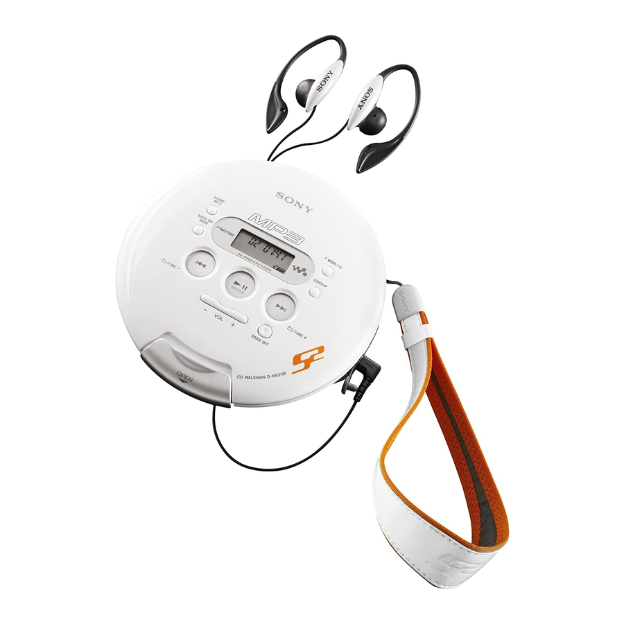
Supplied accessories
AC power adaptor (1) (not supplied with the model for USA)
Headphones (1)
Hand strap (1)
Battery life* (approx. hours)
(When the CD player is used on a flat and stable place.)
Playing time varies depending on how the CD player is used.
When using two Sony alkaline batteries LR6 (SG)
(produced in Japan)
G-PROTECTION
Audio CD
MP3 CD (Recorded at 128 kbps)
RADIO ON
* Measured value by the standard of JEITA (Japan Electronics and
Information Technology Industries Association).
Design and specifications are subject to change without notice.
FM/AM PORTABLE CD PLAYER
US Model
E Model
D-NF007
CDM-3525A
DAX-25A
G-on
G-off
16
11
23
23
35
Advertisement
Table of Contents

Related Manuals for Sony D-NS313F


Summary of Contents for Sony D-NS313F
- Page 1 (When the CD player is used on a flat and stable place.) Radio Playing time varies depending on how the CD player is used. Frequency range When using two Sony alkaline batteries LR6 (SG) 9 kHz step: (produced in Japan) FM: 87.5 - 108 MHz...
-
Page 2: Table Of Contents
COMPONENTS IDENTIFIED BY MARK 0 OR DOTTED LINE WITH MARK 0 ON THE SCHEMATIC DIAGRAMS AND IN THE PARTS LIST ARE CRITICAL TO SAFE OPERATION. REPLACE THESE COMPONENTS WITH SONY PARTS WHOSE PART NUMBERS APPEAR AS SHOWN IN THIS MANUAL OR IN SUPPLEMENTS PUBLISHED BY SONY. -
Page 3: Servicing Notes
D-NS313F SECTION 1 SERVICING NOTES LASER DIODE AND FOCUS SEARCH OPERATION NOTES ON HANDLING THE OPTICAL PICK-UP CHECK BLOCK OR BASE UNIT During normal operation of the equipment, emission of the laser The laser diode in the optical pick-up block may suffer electrostatic... -
Page 4: Disassembly
D-NS313F SECTION 3 DISASSEMBLY • This set can be disassembled in the order shown below. 3-1. DISASSEMBLY FLOW 3-2. UPPER LID ASSY, CABINET (MIDDLE) ASSY (Page 4) 3-3. OPTICAL PICK-UP (CDM-3525A,) MAIN BOARD (Page 5) 3-4. SWITCH BOARD, UPPER LID SUB ASSY (Page 5) Note: Follow the disassembly procedure in the numerical order given. -
Page 5: Optical Pick-Up (Cdm-3525A), Main Board
D-NS313F 3-3. OPTICAL PICK-UP (CDM-3525A), MAIN BOARD 5 optical pick-up (CDM-3525A) 2 wire (flat type) (CN501) 4 Unsolder four lead wires. to optical pick-up 6 MAIN board MAIN board (side A) S812 lever (hold) 1 battery terminal (relay) Note: On installtion MAIN board, adjust S812 and lever (hold). -
Page 6: Electrical Adjustment
D-NS313F SECTION 4 ELECTRICAL ADJUSTMENTS [TUNER SECTION] ): 9kHz step model CLOCK SHIFT ADJUSTMENT AM IF ADJUSTMENT Connection: Adjust for a maximum reading on level meter frequency counter T002 620 (621) kHz MAIN board TP471 (SIFT) ): 9kHz step model TP005 (RFGND (A)) or –... - Page 7 D-NS313F Adjustment and Connecting Location: MAIN BOARD (SIDE A) CN801 IC801 T002: AM IF Adjustment TP002 RV471: (RF(A)) Clock Shift Adjustment IC401 TP005 TP604 IC601 (RF GND(A)) (RF) CT001: AM Tracking Adjustment MAIN BOARD (SIDE B) IC901 TP471 TP473 TP012...
- Page 8 D-NS313F [CD SECTION] Procedure: The CD section adjustments are done automatically in this set. 1. Make a solder bridge to short SL801 (OPEN) on the MAIN board side A. Adjusting Procedure: 2. Connect the oscilloscope to the test point TP604 (RF) and 1.
-
Page 9: Diagrams
D-NS313F SECTION 5 DIAGRAMS • Note for Printed Wiring Boards and Schematic Diagrams • Waverforms IC601 ya XO (CD play mode) Note on Printed Wiring Boards. Note on Schematic Diagrams. • All capacitors are in µF unless otherwise noted. (p: pF) •... -
Page 10: Block Diagram -Cd/Power Section
D-NS313F 5-1. BLOCK DIAGRAM –CD/POWER SECTION– IC602 SDRAM(16M) TU L TUNER DQ0-15 TUNER A0-11 SECTION SECTION TU R 2,3,5,6,8,9,11,12,39, (Page 11) 19-24,27-32 17 16 15 14 36 35 34 (Page 11) 40,42,43,45,46,48,49 IC301 Q602 HEADPHONE AMP OPTICAL PICK-UP 32-21 (CDM-3525A) -
Page 11: Block Diagram - Tuner Section
D-NS313F 5-2. BLOCK DIAGRAM –TUNER SECTION– IC001 INVERTER IC901 Q001 FM RF AMP, FM/AM OSC, T002 FM/AM IF AMP, FM/AM DET, FM MPX, PLL TU VOLUME AM IF FL001 T002 CD/POWER FM/TV RF IN FM IF CF001 (AM IFT) L OUT... -
Page 12: Printed Wiring Board - Main Board (Side A)
D-NS313F 5-3. PRINTED WIRING BOARD – MAIN BOARD (SIDE A) – :Uses unleaded solder. SWITCH BOARD CN802 (Page 17) RB802 Q804 Q803 MAIN BOARD (SIDE A) CN801 C877 X802 RB810 C872 C881 R879 R875 RB811 R820 C813 RB815 RB814 RB812... -
Page 13: Printed Wiring Board - Main Board (Side B)
D-NS313F 5-4. PRINTED WIRING BOARD – MAIN BOARD (SIDE B) – :Uses unleaded solder. • Semiconductor Location MAIN BOARD (SIDE B) VDR802 Ref. No. Location C882 C880 R872 D001 C806 C802 R821 D002 D004 R848 RB806 D871 RB801 C808 D872... -
Page 14: Schematic Diagram - Main Board (1/3)
D-NS313F 5-5. SCHEMATIC DIAGRAM – MAIN BOARD (1/3) – • See page 9 for Waveforms. • See page 18 for IC Block Diagrams. D-NS313F... -
Page 15: Schematic Diagram - Main Board (2/3)
D-NS313F • See page 9 for Waveforms. • See page 18, 19 for IC Block Diagrams. • See page 22 for IC Pin Function Description. 5-6. SCHEMATIC DIAGRAM – MAIN BOARD (2/3) – D-NS313F... -
Page 16: Schematic Diagram - Main Board (3/3)
D-NS313F 5-7. SCHEMATIC DIAGRAM – MAIN BOARD (3/3) – • See page 9 for Waveforms. • See page 20 for IC Pin Function Description. D-NS313F... -
Page 17: Printed Wiring Board - Switch Board
D-NS313F 5-8. PRINTED WIRING BOARD – SWITCH BOARD – :Uses unleaded solder. 5-9. SCHEMATIC DIAGRAM – SWITCH BOARD – MAIN BOARD CN801 (Page 12) SWITCH BOARD CN802 R880 S808 S809 SOUND/ AVLS P MODE/ S871 CN803 S806 RADIO ON/ GROUP... - Page 18 D-NS313F • IC Block Diagrams IC401 BH6575FV-E2 IC001 TB2132FNG VSYS – CONV VSYS PRE-DR PRE-DR DETECT AM OSCIN PROGRAM PHASE COUNTER COMPARATOR FM OSCIN – DC/DC – CONVERTER REFERENCE IFIN DIVIDER TV 1/8 BUFFER FM/AM/TV 1/16 SWITCH FM 1/32 FM/TV 1/2...
- Page 19 D-NS313F IC601 BU9542JKV AVDD1 D CLASS HP LINE AMPLIFIER DGND2 AMPLIFIER TEST VBIAS RESETB SIGNAL 1 BIT DAC AGND1 CLK88 GENERATOR SUBSYQ BUSY SERVO DIGITAL SIGNAL SIGNAL 16K SRAM GENERATOR X8 OVER PROCESSOR SAMPLING DIN/DOUT DIGITAL FILTER VDD_CORE2 FDOUT DQ00...
-
Page 20: Ic Pin Function Description
D-NS313F 5-10. IC PIN FUNCTION DESCRIPTION • IC801 BU18704-S6 (SYSTEM CONTROLLER) Pin No. Pin name Description SEG0 Not used (OPEN) 2 to 21 SEG1 to SEG20 LCD segment output LINEOUT_MUTE Not used (OPEN) EE_SDA/REM_SDA EEPROM data EE_SCL EEPROM clock SYSREQ... - Page 21 D-NS313F Pin No. Pin name Description BATT+ Batt+ terminal voltage monitoring input KEY1 Key matrix detect input KEY2 Key matrix detect input TEST Test mode terminal WREM Wired remotecontroler key detection input SEL_VERSION Select version Connect to GND TEST1 Test mode terminal (not used) P.OFF...
- Page 22 D-NS313F • IC1001 TMP86C808DMG-6F65 (TUNER CONTROLLER) Pin No. Pin name Description – Ground terminal 8MHz clock input XOUT 8MHz clock output TEST Fixed at ground VCPU – Power supply terminal XTIN 75kHz clock input XTOUT 75kHz clock output (OPEN) RESET...
-
Page 23: Exploded Views
D-NS313F SECTION 6 EXPLODED VIEWS NOTE: The components identified by mark 0 • Accessories are given in the last of the • -XX and -X mean standardized parts, so they or dotted line with mark 0 are critical electrical parts list. -
Page 24: Electrical Parts List
D-NS313F Ver. 1.1 SECTION 7 MAIN ELECTRICAL PARTS LIST NOTE: The components identified by mark 0 • SEMICONDUCTORS • Due to standardization, replacements in the or dotted line with mark 0 are critical In each case, u: µ, for example: parts list may be different from the parts for safety. - Page 25 D-NS313F MAIN Ref. No. Part No. Description Remark Ref. No. Part No. Description Remark C420 1-124-635-00 ELECT 220uF 6.3V C815 1-107-826-11 CERAMIC CHIP 0.1uF C872 1-162-916-11 CERAMIC CHIP 12PF C421 1-125-837-91 CERAMIC CHIP 6.3V C874 1-162-970-11 CERAMIC CHIP 0.01uF C450 1-125-837-91 CERAMIC CHIP 6.3V...
- Page 26 D-NS313F MAIN Ref. No. Part No. Description Remark Ref. No. Part No. Description Remark FB402 1-414-813-11 FERRITE, EMI (SMD) (2012) Q474 8-729-028-99 TRANSISTOR DTC114YUA-T106 FB403 1-412-028-11 INDUCTOR 4.7uH Q475 8-729-028-97 TRANSISTOR DTC114TUA-T106 FB404 1-412-028-11 INDUCTOR 4.7uH Q476 8-729-028-99 TRANSISTOR DTC114YUA-T106...
- Page 27 D-NS313F MAIN Ref. No. Part No. Description Remark Ref. No. Part No. Description Remark R902 1-216-797-11 METAL CHIP 1/10W R471 1-216-845-11 METAL CHIP 100K 1/10W R904 1-216-813-11 METAL CHIP 1/10W R472 1-216-829-11 METAL CHIP 4.7K 1/10W R1001 1-414-760-21 FERRITE, EMI (SMD) (1608)
- Page 28 D-NS313F Ver. 1.1 MAIN SWITCH Ref. No. Part No. Description Remark VDR802 1-100-507-91 CERAMIC CHIP 4.7uF 6.3V < VIBRATOR > X001 1-795-926-11 VIBRATOR, CRYSTAL (75kHz) X601 1-813-590-11 VIBRATOR, CERAMIC (16.9344MHz) X801 1-795-926-11 VIBRATOR, CRYSTAL (75kHz) X802 1-813-722-11 VIBRATOR, CERAMIC (8MHz)
- Page 29 D-NS313F MEMO...
-
Page 30: Revision History
D-NS313F REVISION HISTORY Clicking the version allows you to jump to the revised page. Also, clicking the version at the upper right on the revised page allows you to jump to the next revised page. Ver. Date Description of Revision 2006.06...