Table of Contents
Advertisement
Advertisement
Table of Contents

Related Manuals for Topfield TF4000FI


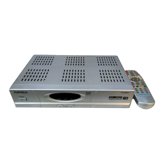
Summary of Contents for Topfield TF4000FI
-
Page 1: Service Manual
TF4000Fi Service Manual 15 March, 2004 Topfield Co., Ltd... -
Page 2: Important
IMPORTANT Note : The design of the satellite receiver is subject to continuous development and improvement. Consequently, this receiver may incorporate minor changes in detail from the information contained in this manual. Warning : These servicing instructions are for use by qualified personnel only. To reduce the risk of electric shock, do not perform any servicing other than that specified in the operating instructions unless you are fully qualified to do so. -
Page 3: Table Of Contents
TABLE OF CONTENTS Page IMPORTANT ...................... 2 1. Safety Instructions ..................5 2. List and Description of The Major Parts ............6 2.1. Main Board ......................6 2.2. Front Board ......................6 3. Block Diagram of The IRD ................7 4. - Page 4 5.5.2. Test the diodes..........................17 5.5.3. Check the Shunt regulator ......................17 5.5.4. Check the Pothocoupler IC......................17 5.5.5. Check the Fuse........................... 17 6. PIN description of The Major Parts ............18 6.1. Main Board ......................18 6.2. Front Board ......................18 6.3.
-
Page 5: Safety Instructions
1. Safety Instructions Read this chapter carefully before servicing the IRD. 1.1 The IRD must be disconnected from the mains plug before it is opened. 1.2 The capacitor inside the SMPS (power supply) can hold charge even if the IRD has been disconnected from the mains plug. -
Page 6: List And Description Of The Major Parts
List and Description of The Major Parts 2.1. Main Board Part Location Part number Function Comment Name Number Tuner module TBMU24311IPP Channel tuning. Or, equivalent part Analog to Digital Conversion. QPSK demodulation. Regulator LM7805 Regulates Tuner 5V Or, equivalent part (with Heat Sink) LNB Power LNBP20PD... -
Page 7: Block Diagram Of The Ird
3. Block Diagram of The IRD... -
Page 8: Block Diagram Of The Main Board
4. Block Diagram of The Main Board... -
Page 9: Test And Repair
5. Test and Repair 5.1. Visual Test - Check whether all the connectors are plugged well. ‘JP4’ of Main Board : power connector. ‘JP5’ of Main Board : connector for Front Board interface ‘JP3’ of Main Board : Connector for SMART Card sub-Board interface (optional). - Check whether the SMPS(power supply) has any damage. -
Page 10: Basic Function Test
5.2. Basic Function Test 5.2.1. No LED is turned on Possible Cause How to Check How to repair Front Board Problem Replace the Front Board with If it works, repair the Front Board. new one which works well in the Otherwise, check the Main Board other IRD and SMPS. -
Page 11: No Picture But The Osd Works
5.2.6. No picture but the OSD works. Possible Cause How to Check How to repair Tuner problem If the signal level of the tuner is Check the antenna signal. very low, it may be a problem of Check the tuner part. the tuner, antenna cable or antenna. -
Page 12: No Sound And/Or No Picture On The Rf Modulator (Cinch Works Well)
5.2.10. No sound and/or no picture on the RF modulator (Cinch works well) Possible Cause How to Check How to repair RF channel is selected Check channel Select the correct channel. incorrectly. selection. modulator Replace the RF modulator with Replace it with new one. problem. -
Page 13: The Advanced Test Of Main Board
5.3. The Advanced Test of Main Board. 5.3.1. Voltages on important point - Voltage at JP4 in page 8 (of schematic diagram) Minimum Nominal Maximum Comment number voltage voltage voltage +28V +30V +32V +20V +22V +23V +16V +17V +18V +7.6V +8.4V not used not used... -
Page 14: System Clock
Schematic page 4. 5.3.3. System Clock Schematic page 3 VCXO1 generates the system clock. The ‘SCLK’ signal is 27.000MHz clock signal . If the color of the picture disappear , the ‘SCLK’ signal may be different from 27.000MHz or the VCXO1 have bad quality. -
Page 15: Lnb Power
nothing happens in the receiver, check the download cable and the PC. The pin2 and pin3 of the download cable should be crossed. - Check point 1 - Check the download cable and the PC with a new receiver. - Check point 2 - Check the error code on the display of the Front Board. -
Page 16: Rf Modulator
Set the LNB voltage to Horizontal - Check Point – Check level of U3.5 whether logically ‘HIGH’ ( about 3V ). If logically ‘LOW’ ( about 0V) then check the line from U5 (IBM39STB02500 ) and U3.5. Check level of U3.6 whether logically ‘HIGH’ ( about 3V ). If logically ‘LOW’ ( about 0V) then check the line from U5 (IBM39STB02500) and U3.6. -
Page 17: The Advanced Test Of Smps
5.5. The Advanced Test of SMPS. Caution -------------------------------------- ------------------------------------------- I. The SMPS must be disconnected from the mains plug to test. II. The capacitor inside the SMPS (power supply) can hold charge even if the IRD has been disconnected from the mains plug. To handle SMPS, wait until the capacitor is discharged. -
Page 18: Pin Description Of The Major Parts
6. PIN description of The Major Parts 6.1. Main Board Tuner Module TBMU24311IPP Regulator LM7805 LNB Power Switching IC LNBP20PD CPU, Demux and Decoder IBM39STB02500 Flash Memory SST39VF800A EEPROM 24LC02B-SN SDRAM K4S641632D Reset IC ELM9727NBA Regulator LD1117ADT18 Regulator MIC39100-2.5BS Regulator 78L12 RS232 Driver MAX232... -
Page 20: General Description
February 1995 LM78XX Series Voltage Regulators General Description The LM78XX series of three terminal regulators is available of external components It is not necessary to bypass the with several fixed output voltages making them useful in a output although this does improve transient response Input wide range of applications One of these is local on card bypassing is needed only if the regulator is located far from regulation eliminating the distribution problems associated... - Page 21 LNBP10 SERIES - LNBP20 input pin is available (EXTM). An appropriate DC IMPEDANCE. If the overload is still present, the blocking capacitor must be used to couple the protection circuit will cycle again through t modulating signal source to the EXTM pin. When ton until the overload is removed.
- Page 22 IBM39STBx25xx Preliminary STBx25xx Digital Set-Top Box Integrated Controllers 1.6.4.10 Real Time Clock / Front Panel Controller The Real Time Clock (RTC) counts seconds, minutes, hours, and days. Programmable alarms can be set to interrupt the CPU, allowing the CPU to wake up when required to perform functions such as programming a VCR.
- Page 23 IBM39STBx25xx STBx25xx Digital Set-Top Box Integrated Controllers Preliminary Table 1-1. Signals Sorted by Signal Name I/O Signal Name Ball Number BI_CS0 BI_CS1 BI_CS2 BI_CS3 BI_DATA0 BI_DATA1 BI_DATA10 BI_DATA11 BI_DATA12 BI_DATA13 BI_DATA14 BI_DATA15 BI_DATA2 BI_DATA3 BI_DATA4 BI_DATA5 BI_DATA6 BI_DATA7 BI_DATA8 BI_DATA9 BI_OE BI_READY BI_RW...
- Page 24 IBM39STBx25xx Preliminary STBx25xx Digital Set-Top Box Integrated Controllers Table 1-1. Signals Sorted by Signal Name I/O Signal Name Ball Number DAC1_AGND1 DAC1_AGND2 DAC1_AVDD0 DAC1_AVDD1 DAC1_AVDD2 DAC1_AVDD3 DAC1_VOUT1 DAC1_CREF_OUT DAC1_VOUT2 DAC1_GREF_OUT DAC1_VOUT3 DAC1_RREF_OUT DAC1_VREF_IN DAC2_AGND0 DAC2_AGND1 DAC2_AGND2 DAC2_AVDD0 DAC2_AVDD1 DAC2_AVDD2 DAC2_AVDD3 DAC2_VOUT1 DAC2_CREF_OUT DAC2_VOUT2...
- Page 25 IBM39STBx25xx STBx25xx Digital Set-Top Box Integrated Controllers Preliminary Table 1-1. Signals Sorted by Signal Name I/O Signal Name Ball Number AA21 AA23 Product Overview Stbx25_Overview.fm.02 Page 46 of 890 May 31, 2002- IBM Confidential...
- Page 26 IBM39STBx25xx Preliminary STBx25xx Digital Set-Top Box Integrated Controllers Table 1-1. Signals Sorted by Signal Name I/O Signal Name Ball Number AB22 AC10 AC14 AC18 AC23 GPIO0 GPIO1 GPIO10 GPIO11 GPIO12 GPIO13 GPIO14 GPIO15 GPIO16 GPIO17 GPIO18 GPIO19 GPIO2 GPIO20 GPIO21 GPIO22 GPIO23 GPIO24...
- Page 27 IBM39STBx25xx STBx25xx Digital Set-Top Box Integrated Controllers Preliminary Table 1-1. Signals Sorted by Signal Name I/O Signal Name Ball Number I2C0_SCL I2C0_SDA INT0 INT1 INT2 RW_HALT RW_TCK RW_TDI RW_TDO RW_TMS RW_TRST SC0_CLK SC0_DETECT SC0_IO SC0_RESET SC0_VCC SC1_CLK SC1_DETECT SC1_IO SC1_RESET SC1_VCC SD0_ADDRESS0 SD0_ADDRESS1...
- Page 28 IBM39STBx25xx Preliminary STBx25xx Digital Set-Top Box Integrated Controllers Table 1-1. Signals Sorted by Signal Name I/O Signal Name Ball Number SD0_CLK SD0_CS0 SD0_DATA0 SD0_DATA1 SD0_DATA10 SD0_DATA11 SD0_DATA12 SD0_DATA13 SD0_DATA14 SD0_DATA15 SD0_DATA2 SD0_DATA3 SD0_DATA4 SD0_DATA5 SD0_DATA6 SD0_DATA7 SD0_DATA8 SD0_DATA9 SD0_DQMH SD0_DQML SD0_RAS SD0_WE SD1_ADDRESS0...
- Page 29 IBM39STBx25xx STBx25xx Digital Set-Top Box Integrated Controllers Preliminary Table 1-1. Signals Sorted by Signal Name I/O Signal Name Ball Number SD1_CAS AA16 SD1_CLK AA15 SD1_CS0 AC15 SD1_DATA0 SD1_DATA1 SD1_DATA10 AC13 SD1_DATA11 AB13 SD1_DATA12 AA13 SD1_DATA13 AB14 SD1_DATA14 AA14 SD1_DATA15 SD1_DATA2 SD1_DATA3 SD1_DATA4 AA10...
- Page 30 IBM39STBx25xx Preliminary STBx25xx Digital Set-Top Box Integrated Controllers Table 1-1. Signals Sorted by Signal Name I/O Signal Name Ball Number VDD2 VDD2 VDD2 VDD2 VDD2 VDD2 VDD2 VDD2 VDD2 VDD2 VDD2 VDD2 VDD2 VDD2 VDD2 VDD2 Stbx25_Overview.fm.02 Product Overview May 31, 2002- IBM Confidential Page 51 of 890...
- Page 31 IBM39STBx25xx Preliminary STBx25xx Digital Set-Top Box Integrated Controllers 1.10 Mechanical Information Package Diagram Top of Package (BGA Side Down) IBM P/N XXXXXXX ZZWWMMMM Date Code IBM39 STBx25xx xxx xxx 0.25 OEM P/N 1.22 15.5 0.15 .610 27.94 1.27 .050 E52P SUBSTRATE GLOB Cavity...
- Page 32 2 Mbit / 4 Mbit / 8 Mbit Multi-Purpose Flash SST39LF200A / SST39LF400A / SST39LF800A SST39VF200A / SST39VF400A / SST39VF800A Data Sheet UNCTIONAL LOCK IAGRAM SuperFlash X-Decoder Memory Memory Address Address Buffer & Latches Y-Decoder I/O Buffers and Data Latches Control Logic DQ 15 - DQ 0 360 ILL B1.2...
- Page 33 Features • Low-Voltage and Standard-Voltage Operation – 5.0 (V = 4.5V to 5.5V) – 2.7 (V = 2.7V to 5.5V) – 2.5 (V = 2.5V to 5.5V) – 1.8 (V = 1.8V to 5.5V) • Internally Organized 128 x 8 (1K), 256 x 8 (2K), 512 x 8 (4K), 1024 x 8 (8K) or 2048 x 8 (16K) •...
- Page 34 K4S641632D CMOS SDRAM PIN CONFIGURATION (Top view) DQ15 DQ14 DQ13 DQ12 DQ11 DQ10 LDQM N.C/RFU UDQM A10/AP 54Pin TSOP (II) (400mil x 875mil) (0.8 mm Pin pitch) PIN FUNCTION DESCRIPTION Name Input Function System clock Active on the positive going edge to sample all inputs. Disables or enables device operation by masking or enabling all inputs except Chip select CLK, CKE and L(U)DQM...
- Page 36 LD1117 SERIES CONNECTION DIAGRAM (top view) SOT-223 SO-8 TO-220FM TO-220 DPAK NOTE: The TAB is connected to the V ORDERING CODES OUTPUT SOT-223 SO-8 DPAK TO-220 TO-220FM VOLTAGE LD1117S12 LD1117D12 (*) LD1117DT12 LD1117V12 (*) LD1117F12 (*) 1.2 V LD1117S18 LD1117D18 LD1117DT18 LD1117V18 LD1117F18...
-
Page 37: Pin Description
MIC39100/39101/39102 Micrel Pin Configuration MIC39100-x.x Fixed SOT-223 (S) 8 GND 8 GND MIC39101-x.x MIC39102 Fixed Adjustable SOP-8 (M) SOP-8 (M) Pin Description Pin No. Pin No. Pin No. Pin Name Pin Function MIC39100 MIC39101 MIC39102 Enable (Input): CMOS-compatible control input. Logic high = enable, logic low or open = shutdown. - Page 38 L78L00 CONNECTION DIAGRAM AND ORDERING NUMBERS (top view) pin 1 = V pin 2 = GND pin 3 = V SO-8 SOT-89 TO-92 BOTTOM VIEW ORDERING NUMBERS Type SO-8 TO-92 SOT-89 (T&R) Output Voltage L78L33AC L78L33ACD L78L33ACZ L78L33ACUTR 3.3 V L78L33AB L78L33ABD L78L33ABZ...
- Page 39 +5V-Powered, Multichannel RS-232 Drivers/Receivers +5V INPUT TOP VIEW 2 +10V +5V TO +10V VOLTAGE DOUBLER -10V +10V TO -10V VOLTAGE INVERTER MAX220 MAX232 400k MAX232A TTL/CMOS RS-232 INPUTS 400k OUTPUTS DIP/SO R1 I TTL/CMOS RS-232 CAPACITANCE (µF) OUTPUTS INPUTS DEVICE MAX220 MAX232 MAX232A...
- Page 40 Philips Semiconductors Preliminary specification Low power audio DAC UDA1334TS PINNING SYMBOL PAD TYPE DESCRIPTION 5 V tolerant digital input pad; note 1 bit clock input 5 V tolerant digital input pad; note 1 word select input DATAI 5 V tolerant digital input pad; note 1 serial data input digital supply pad digital supply voltage...
-
Page 42: Block Diagram
TSOP48..SB1 Vishay Telefunken Photo Modules for PCM Remote Control Systems Available types for different carrier frequencies Type Type TSOP4830SB1 30 kHz TSOP4833SB1 33 kHz TSOP4836SB1 36 kHz TSOP4837SB1 36.7 kHz TSOP4838SB1 38 kHz TSOP4840SB1 40 kHz TSOP4856SB1 56 kHz Description The TSOP48..SB1 –... - Page 43 TSOP48..SB1 Vishay Telefunken Dimensions in mm 16777 www.vishay.com Document Number 82108 6 (7) Rev. 6, 29-Mar-01...
- Page 44 www.fairchildsemi.com KA1L0380B/KA1L0380RB/ KA1M0380RB/KA1H0380RB Fairchild Power Switch(FPS) Features Description • Precision fixed operating frequency The Fairchild Power Switch(FPS) product family is specially • (50KHz) designed for an off line SMPS with minimal external KA1L0380B/KA1L0380RB • (67KHz) components. The Fairchild Power Switch(FPS) consist of high KA1M0380RB •...
- Page 45 www.fairchildsemi.com KA431/KA431A/KA431L Programmable Shunt Regulator Features Description • Programmable output voltage to 36 volts The KA431/KA431A/KA431L are three-terminal adjustable • Low dynamic output impedance 0.20 typical regulator series with a guaranteed thermal stability over • Sink current capability of 1.0 to 100mA applicable temperature ranges.
-
Page 46: Schematic Diagrams
7. Schematic Diagrams 7.1. Schematic diagram of Front Board - see next page. -
Page 48: Schematic Diagram Of Main Board
7.2. Schematic diagram of Main Board - see next page. -... -
Page 61: Schematic Diagram Of Smps (Power Supply)
7.3. Schematic diagram of SMPS (power supply) - see next page. -...