Table of Contents
Advertisement
Quick Links
Download this manual
See also:
Instruction Manual
SERVICE MANUAL
SERVICE MANUAL
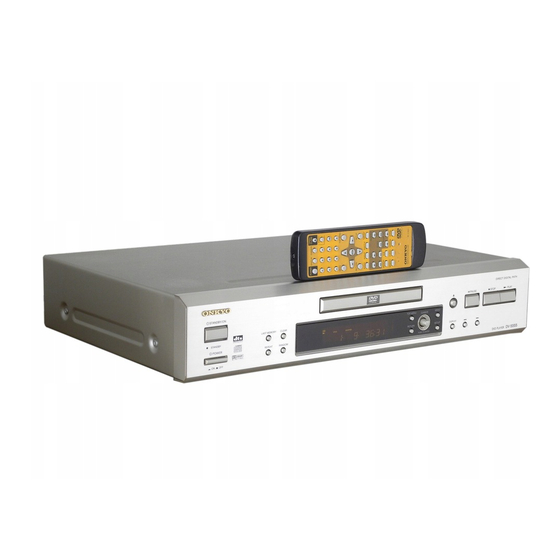
DVD Player
DV-S555
Black, Silver and Golden models
BMDD
120V AC, 60Hz
BMUP, SMUP
230 -240V AC, 50/60Hz
BMUT, BMUS,
100 - 240V AC, 50/60Hz
GMUT, GMUR
SAFETY-RELATED COMPONENT
WARNING!!
COMPONENTS IDENTIFIED BY MARK
SCHEMATIC DIAGRAM AND IN THE PARTS LIST ARE
CRITICAL FOR RISK OF FIRE AND ELECTRIC SHOCK.
REPLACE THESE COMPONENTS WITH ONKYO
PARTS WHOSE PART NUMBERS APPEAR AS SHOWN
IN THIS MANUAL.
MAKE LEAKAGE-CURRENT OR RESISTANCE
MEASUREMENTS TO DETERMINE THAT EXPOSED
PARTS ARE ACCEPTABLY INSULATED FROM THE
SUPPLY CIRCUIT BEFORE RETURNING THE
APPLIANCE TO THE CUSTOMER.
ON
OPEN/CLOSE
TV
ON/STANDBY
STANDBY
ANGLE
AUDIO
SUBTITLE
LAST M
COND. M
DIMMER
DISPLAY
TOP MENU
MENU
CH -
CH +
VOL +
ENTER
VOL -
RETURN
SETUP
TV/ VCR
PAUSE
STOP
PLAY
FR
FF
DOWN
UP
STEP/SLOW
+
1
2
3
-
4
5
6
FUNCTION M
7
8
9
SEARCH
CLEAR
+10
0
RANDOM REPEAT
A-B
PROGRAM
REMOTE CONTROLLER RC- 449 DV
DVD
TV
RC-449DV
U.S.A., Canadian
models only
ON THE
DV-S555
Ref. No.3685
072001
ON
OPEN/CLOSE
TV
ON /ST ANDB Y
STANDBY
ANGLE
AUDIO
SUBTITLE
LAST M
COND. M
DIMMER
DISPLAY
TOP MENU
MENU
CH-
CH+
VOL +
ENTER
VOL -
RETURN
SETUP
TV/ VCR
PAUSE
STOP
PLAY
FR
FF
DOWN
UP
STEP/SLOW
+
1
2
3
-
4
5
6
FUNCTION M
7
8
9
SEARCH
CLEAR
+10
0
RANDOM REPEAT
A-B
PROGRAM
REMOTE CONTROLLER RC- 450 DV
DVD
DVD
TV
TV
RC-450DV
Other models
Advertisement
Table of Contents

Related Manuals for Onkyo DV-S555


Summary of Contents for Onkyo DV-S555
-
Page 1: Dvd Player
COMPONENTS IDENTIFIED BY MARK ON THE SCHEMATIC DIAGRAM AND IN THE PARTS LIST ARE CRITICAL FOR RISK OF FIRE AND ELECTRIC SHOCK. REPLACE THESE COMPONENTS WITH ONKYO PARTS WHOSE PART NUMBERS APPEAR AS SHOWN IN THIS MANUAL. MAKE LEAKAGE-CURRENT OR RESISTANCE... -
Page 2: Specifications
DV-S555 SPECIFICATIONS DVD Player Power supply North American models: AC 120 V, 60 Hz Other models: AC 100 - 240 V, 50/60 Hz Power consumption North American models: 14 W Other models: 15 W Weight 3.4 kg, 7.1 lbs. External dimensions 435 x 91 x 312 mm (W/H/D), 17-1/8"... -
Page 3: Service Note
DV-S555 SERVICE NOTE PRECAUTIONS 1.Ground for the work-desk. Place a conductive sheet such as a sheet of copper (with impedance lower than 10Mohm) on the work-desk and place the set on the conductive sheet so that the chassis. 2.Grounding for the test equipments and tools. -
Page 4: Panel View
Press to open and close the disc tray. surge that might interfere with other electrical equipment on PAUSE button the same circuit. If this is a problem, plug the DV-S555 into a Press during playback to pause. Press again to resume playback. different electrical circuit. -
Page 5: Rear Panel
DV-S555 PANEL VIEW Display V C D REPEAT LAST TITLE CHAPTER TRACK REMAIN COND. 10 11 12 / indicator LAST indicator Inserted disc indicator COND. indicator TITLE indicator D indicator 4. Angle icon indicator DTS indicator 5. CHAPTER/TRACK indicator GUI indicator... -
Page 6: Remote Controller
DV-S555 PANEL VIEW Remote controller OPEN/CLOSE ON/STANDBY FR/FF buttons STANDBY ANGLE AUDIO SUBTITLE During playback of DVD and Video CD, press to perform fast LAST M COND. M DIMMER DISPLAY forward scanning or to perform fast reverse scanning of DVD and Video CD. -
Page 7: Exploded View
DV-S555 EXPLODED VIEW To DVD Mechanism E701 E702 : Torque 1.6+/-0.5kgf S731 E903... - Page 9 DV-S555 EXPLODED VIEW (LOADING MECHANISM) Daifree GEM1036 To DVDM CN151 Lubricating Oil GYA1001 Lubricating Oil GYA1001 LOADING MECHANISM ASSY PARTS LIST DESCRIPTION REF.NO. PART NO. DESCRIPTION REF.NO PART NO. VNL1918 Float base DVD VNP1836 Loading PC board assy VNL1919 Drive cam...
-
Page 10: Block Diagram
DV-S555 BLOCK DIAGRAM Overall Main circuit PCB IC712 DB-VPB301 MSM51V17805D-60TS 16M DRAM CN151 (RF) (RF) (26P) (26P) (RF) (VD) (VD) Spindle DSP RF ROMXA SD0-SD7 Motor 57-60 IC101 (RF) 63-66 (AD) LA9701M RF IC IC701 CDDATA Pickup PE5108A Assembly DVD Decoder... - Page 11 DV-S555 (RF) (VD) : RF SIGNAL ROUTE : VIDEO DATA SIGNAL ROUTE : C SIGNAL ROUTE (AD) : AUDIO DATA SIGNAL ROUTE : VIDEO SIGNAL ROUTE : R SIGNAL ROUTE : AUDIO SIGNAL ROUTE : V SIGNAL ROUTE : G SIGNAL ROUTE...
-
Page 12: Mechanism Section
DV-S555 BLOCK DIAGRAM Mechanism section PICKUP ASSY-S CN120 (RF) (RF) (RF) (RF) SPINDLE MOTOR CN251 : VXM1088 VKN1272 STEPPING MOTOR (CARRIAGE) VKN1277 VKN1264 : VXM1090 SSIB ASSY (VWG2292) CN52 S101 : VSK1011 CN602 S2B-PH-K LOADING MOTOR ASSY : VXX2505 CN601... -
Page 13: Schematic Diagram
DV-S555 SCHEMATIC DIAGRAM (Page 1) Main circuit PC board Page 2 Page 2 (RF) Page 2 CN151 (RF) CN52 For Mecha connector... - Page 14 DV-S555 (RF) : RF SIGNAL ROUTE : RF (VIDEO) SIGNAL ROUTE TC7SZU04F Page 2 IC304 : RF (AUDIO) SIGNAL ROUTE (AD) : AUDIO DATA SIGNAL ROUTE Page 3 : FOCUS SERVO LOOP LINE : TRACKING SERVO LOOP LINE 3.3k : SLIDER SERVO LOOP LINE...
- Page 15 DV-S555 SCHEMATIC DIAGRAM (Page 2) VYW1853 470k CN512 MECHA Page1 page 1 IC201 To CN15 Page 4...
- Page 16 DV-S555 (RF) : RF SIGNAL ROUTE : RF (VIDEO) SIGNAL ROUTE TC7SZU04F Page 2 IC304 : RF (AUDIO) SIGNAL ROUTE (AD) : AUDIO DATA SIGNAL ROUTE Page 3 : FOCUS SERVO LOOP LINE : TRACKING SERVO LOOP LINE 3.3k : SLIDER SERVO LOOP LINE...
- Page 17 DV-S555 SCHEMATIC DIAGRAM (Page 3) To SCRUT 7,21, 68, 188P IC712 4M MSM51V17805D-60TS (SOP) (VD) Page 1 IC201 Page 1 R334 Page 2/ IC601 to Page 1 Page 3 IC 801 Page 2 IC 601 Page 1 IC 201...
- Page 18 DV-S555 SCHEMATIC DIAGRAM (Page 3) PAL model only IC806 : RF (VIDEO) SIGNAL ROUTE (VD) : VIDEO DATA SIGNAL ROUTE (AD) : AUDIO DATASIGNAL ROUTE : AUDIO SIGNAL ROUTE : AUDIO (DIGITAL) SIGNAL ROUTE DCS2 from AV1 88p IC801 (VD)
- Page 19 DV-S555 SCHEMATIC DIAGRAM (Page 4) (VD) (VD) Page 2...
- Page 20 DV-S555 (VD) : VIDEO DATASIGNAL ROUTE : V SIGNAL ROUTE : Y SIGNAL ROUTE : C SIGNAL ROUTE : R SIGNAL ROUTE : G SIGNAL ROUTE : B SIGNAL ROUTE : AUDIO SIGNAL ROUTE page 2 FR CPU page 3...
- Page 21 DV-S555 DV-S555 SCHEMATIC DIAGRAMS Output Terminal PC board P 7 0 1 A S C K 2 2 S C K N A A R - 7 1 8 1 C 3 6 1 2 3 2 S O 2 1...
-
Page 22: Schematic Diagrams
DV-S555 SCHEMATIC DIAGRAMS Output Terminal PC board P 7 0 1 A S C K N A A R - 7 1 8 1 S C K 2 2 C 3 6 1 2 3 2 S O 2 3 2 S O 2 1... - Page 23 DV-S555 P 3 5 3 S W + 5 V C O A X I A L _ O U T Q 2 0 4 Q 2 0 5 R N 1 4 0 7 R N 2 4 0 3...
- Page 24 DV-S555 DV-S555 SCHEMATIC DIAGRAMS Standby LED PC board Display circuit PC board NADIS-7183A T o P 9 0 2 ( O u t p u t t e r m i n a l P C b o a r d )
- Page 25 DV-S555 SCHEMATIC DIAGRAMS Display circuit PC board NADIS-7182A Q 7 0 5 R 7 4 7 R 7 4 8 3 9 0 4 7 0 R e m o t e S e n s o r D e s t i n a t i o n...
- Page 26 DV-S555 N A V D - 7 1 8 7 Q 2 5 9 2 S D 6 5 5 R 2 7 9 R 2 8 0 Q 2 6 0 Q 2 5 8 2 S D 6 5 5...
- Page 27 DV-S555 PC BOARD CONNECTION DIAGRAM NAPS-7212 Inlet terminal PC board P982A P982B NAAR-7181 Main circuit PC board P104 V+12V VSEL1 NAVD-7181 <MP> model only CN120 CN251 VSEL2 IC701 GNDV1 GNDV2 SCART IC201 GNDV3 +3.3V GNDV4 IC351 SW+5V GNDV5 V+12V AUDIO L...
-
Page 28: Printed Circuit Board View
DV-S555 PRINTED CIRCUIT BOARD VIEW CN102 PICKUP ASSY Bottom pattern and bottom silk CN106 CN601... - Page 29 DV-S555 PRINTED CIRCUIT BOARD VIEW Top pattern and top silk...
- Page 30 PRINTED CIRCUIT BOARD VIEWS U2:Display circuit PC board (NADIS-7182) P731 Q703B J710 P701B J709 PLAY STOP OPEN P710A SETUP D705 D704 D703 PAUSE S711 S710 TOP-MENU S709 S703 S701 J712 J706 DISPLAY S702 S704 MENU RETURN S707 S706 S705 Component side view Display circuit PC board (NADIS-7182) Q709 Q710...
- Page 31 DV-S555 D707 NCDIS-7182 25137182 D706 J748 J747 Q724 J746 Q723 TOP-MENU LAST_MEMORY CLEAR J735 R785 S701 Q702A S712 S715 Q705 J737 J736 J733 Q705 S713 S714 J734 S702 RANDOM REPEAT MENU J739 Q702A Q706 R714 Q707 Q708 R709 Q706...
- Page 32 DV-S555 PRINTED CIRCUIT BOARD VIEWS U8: SCART terminal PC board <MUP> only E201A E201B P251 J318 J317 C254 Q262 Q261 Q260 J302 J301 J304 25137187 J305 NCVD-7187 J303 Component side view R262 Q254 R261 C261 R264 R263 C259 R260 R257...
- Page 33 DV-S555 15mm PRINTED CIRCUIT BOARD VIEWS U1:Output terminal PC board (NAAR-7181A) P902 CN102 MAIN_MCON_DL C910 CN102 C906 C902 C908 P351C C904 M+6V J163 C911 MGND C913 J164 J105 J188 J213 V+12V J225 J165 J189 J214 J190 D902 C452 M+6V J148...
- Page 34 DV-S353 Output terminal PC board C901 C909 C907 D901 C905 C903 R901 C914 R902 R502 Q302 Q351 Q902 Q351 Q401 R506 Q403 Q404 R301 Q405 Q204 Q205 Q202 Q203 Q201 Q201 Soldering side view...
- Page 35 DV-S555 PRINTED CIRCUIT BOARD VIEWS U3:Standby LED PC board D722 S722 S721 R771 R772 JL771B R774 R773 R541 Q721 D721 Soldering side view Component side view U6: Power switch PC board U9: AC inlet terminal PC board P981A P981A S991...
-
Page 36: Printed Circuit Board Parts List
DV-S555 PRINTED CIRCUIT BOARD PARTS LIST Output terminal PC board (NAAR-7181B-1A/1B/1C/1D/1) CIRCUIT NO. PART NO. DESCRIPTION CIRCUIT NO. PART NO. DESCRIPTION Sockets Q201 22241623R2 MM1540BF CN102,CN106 25052610 NSCT-30P-2507 Q251 222840531R2O TC4053BF <UP> P104 25052344 NSCT-7P2241 or Q252 222740007R2O TC74HCT00AF <UP>... - Page 37 DV-S555 PRINTED CIRCUIT BOARD PARTS LIST Display circuit PC board (NADIS-7182B-1A/1B/1C/1D/1E) AC inlet terminal PC board (NAPS-7212B-1A/1B/1C/1D/1B) CIRCUIT NO. PART NO. DESCRIPTION CIRCUIT NO. PART NO. DESCRIPTION Terminal Q701 22241727R3 MPD780232GC-045-8BT P981A 25056006 NPLG-2P956, inlet <MD> Q706 22241713R2 BD4742G 25056027...
- Page 38 DV-S555 Disassembly of the Traverse Mechanism Assy Remove the top cover and Tray Panel. Remove the Loading Mechanism Assy (Screws 4). Remove the Tray panel and Front Panel. Remove a screw. Remove the Bridge (Screw 1). Cautions: Screw is locked with Silicone Adhesive.
- Page 39 DV-S555 FL TUBE VIEW Pin connection DVD-AUDIO DVD-AUDIO VCD PBC 3D 3D PAL PAL RANDOM RANDOM MEMORY MEMORYALL ALL REPEAT REPEAT 1A-B 1A-B LFE LAST LAST DISC DISC TITLE TITLEGROUP GROUP CHAPTER CHAPTERTRACK TRACKTEXT TEXT TOTAL TOTALREMAIN REMAIN D.MIX D.MIX COND.
- Page 40 DV-S555 MICROPROCESSOE TERMINAL DESCRIPTION MPD780232GC-041-8BT Pin No. Symbol Function Description Pin No. Symbol Function Description Vdd1 Vdd1 Power supply, +5V P45/FIP37 SMP192LED Sampling rate 192 LED control pin Vss1 Vss1 Ground pin P44/FIP36 SMP96LED Sampling rate 96 LED control pin...
-
Page 41: Packing View
DV-S555 PACKING VIEW 21,22, 23,24 10,21 RC-449DV <D> RC-450DV <MUP/MUT/ MUS/MUR> <UT,US,UR> 17 <MUP> Front side... -
Page 42: Packing Parts List
DV-S555 PACKING PARTS LIST REF. REF. PART NO. DESCRIPTION PART NO. DESCRIPTION 29091986 Pad ass'y 2010380 S cord 29100037-1A Poly bag, 650 x 500 2010368 or YAF11-0697 or TPX3000 29110098 Tape, W50 3M NO 371 2010360 RGB cord <MUP> 29100097-1A Polybag, 320 x 250 253296HIT AC-UC-2, Power cord <MDD>... -
Page 43: Upgrade Firmware
1-2-3 Then the power and standby switches are turn on. 1-1-4 Run the data writing program. EX) Save the program above in C:DV-S555 folder. The program name are B1BK1048.SZ0, Down.bat, down, ok_down.exe, ok_down Open the DOS window Key input "cd DV-S555" and then push the ENTER key. - Page 44 DV-S555 UPGRADE FIRMWARE PAUSE STOP 2. Setting the Region code. PLAY DOWN 2-1 Turn on the power switch and standby switch is turned on. STEP/SLOW 2-2 Select a regional code. (Using the remote controller RC-449DV Part number 24140449) * MDD1N and MJJ2N are automatically chosen. (Automatically witting)
- Page 45 DV-S555 IC BLOCK DIAGRAM / TERMINAL DESCRIPTION TC4053BF Triple 2-Channel multiplexer / demultiplexer 1Y 1 16 V 0Y 2 15 Y-COM X-COMMON 1Z 3 14 X-COM I / O O / I Z-COM 4 13 1X 0Z 5 12 0X...
- Page 46 DV-S555 IC BLOCK DIAGRAM / TERMINAL DESCRIPTION ADV7172KST (Video Encoder : IC861) 47 46 45 44 43 42 41 40 39 38 37 COMP1 DAC A DAC B DAC C DACD CSO_HSO DAC E 13 14 15 16 17 18 19 20 21 22 23 24...
- Page 47 DV-S555 . s l . s l l r t 0 " . " l a i t s i - l l i l p s " " l l t i c t s i - l l i l p "...
- Page 48 DV-S555 IC TERMINAL DESCRIPTION PCM1742KE Name Pin Function Audio data bit clock input DATA Audio data digital input DATA L-channel and R-channel Audio data LRCK latch enable input DGND Digital ground LRCK Digital power supply +3.3V DGND Analog power supply +5V...
-
Page 49: Ic Block Diagram
DV-S555 IC BLOCK DIAGRAM MM1540BFBE (75 ohm x 2 Driver for DVD (6ch / 9dB)) Block diagram Vcc2 Vcc1 75ohm VOUT Driver +9dB YC MIX 75ohm COUT Driver +9dB VEE2 -6dB 75ohm YOUT1 YIN1 Driver +9dB VEE2 MUTE1 VEE2 MUTE2... - Page 50 DV-S555 IC BLOCK DIAGRAM / TERMINAL DESCRIPTION M65774BFP (MPED2 Decoder : IC801) Block Diagram 16M bit SDRAM SDRAM Bit Streem Descrambler Controller Bit Streem Input Interface Video Decoder Sub-picture Decoder Internal Display Processor Special Playback 16M DRAM Processor Host Video Output...
- Page 51 DV-S555 Pin Function Pin Function n i l n i l n i l h SDRAM n i l n i l n i l n i l h SDRAM n i l n i l h DRAM n i l...
- Page 52 DV-S555 No. Pin Name I/O Pin Function No. Pin Name I/O Pin Function 41 HA9 Address input port 83 VDD Power supply 42 GND Ground 84 VSYNC Vertical sync. Signal output 43 CDMCK Connect to ground 85 HSYNC Horizontal sync. Signal output...
- Page 53 DV-S353 IC BLOCK DIAGRAM / TERMINAL DESCRIPTION LC78652W (Servo DSPY : IC201) Block Diagram SLDO Servo TILTE 8bit 8bit SPDO Processor RF_PH (16 16+32 32) TBAL RF_BH TILTDO AUXO JITT HFLIO Track Counter FAST Event Counter PP2/EVENT DVDSYEQ FG Counter SLCIST1,2 34,35 EFMIN...
- Page 54 DV-S555 IC BLOCK DIAGRAM / TERMINAL DESCRIPTION r r i t i r l a i t f i l l i l i f t l i f t l i f t l i f l l i...
- Page 55 DV-S555 IC BLOCK DIAGRAM / TERMINAL DESCRIPTION Pin Function t f i l l i t t i y t i t l i a i l t l i...
- Page 56 DV-S555 IC BLOCK DIAGRAM BU2288FV (CLOCK GENERATOR) VDD2 33.8688MHz VSS2 CLK33M FSEL1 L or NC (pull up) 27MHz CLK27M TEST CLK16M 16.9344MHz AVDD DVDD AVSS DVSS 24.576 or 22.5792MHz XTALOUT CLK512FS XTALIN 16.9344 or 36.864MHz CLKA BU2288FV...
- Page 57 DV-S555 IC BLOCK DIAGRAM/ TERMINAL DESCRIPTION BA6664FM (Spindle Motor Driver : IC251) Block diagram 1,3,5,6 Driver Gain switch Gain control Current sense amp HALL AMP Torque Short brake Brake mode HALL BIAS Pin No. Pin name Function Pin No. Pin name...
- Page 58 DV-S555 IC BLOCK DIAGRAM / TERMINAL DESCRIPTION PD6345A (Syatem control CPU : IC601) Pin Function utput...
- Page 59 DV-S555 t i s t i s d i l t i s l l o l l o " r " L " : " L L " : " t s i L " : " c t i L "...
- Page 60 DV-S555 i t l c t i c t i " " L " ) " l a i l a i l a i c t i l a i l e l c t i c t i...
- Page 61 DV-S555 x i f x i f...
- Page 62 Sales & Product Planning Div. : 2-1, Nisshin-cho, Neyagawa-shi, OSAKA 572-8540, JAPAN Tel: 072-831-8111 Fax: 072-833-5222 ONKYO U.S.A. CORPORATION 18 Park Way, Upper Saddle River, N.J. 07458, U.S.A. Tel: 201-785-2600 Fax: 201-785-2650 E-mail: onkyo@onkyousa.com ONKYO EUROPE ELECTRONICS GmbH Industriestrasse 20, 82110 Germering, GERMANY Tel: 089-849-320 Fax: 089-849-3265 E-mail: info@onkyo.de...