Table of Contents
Advertisement
SERVICE MANUAL
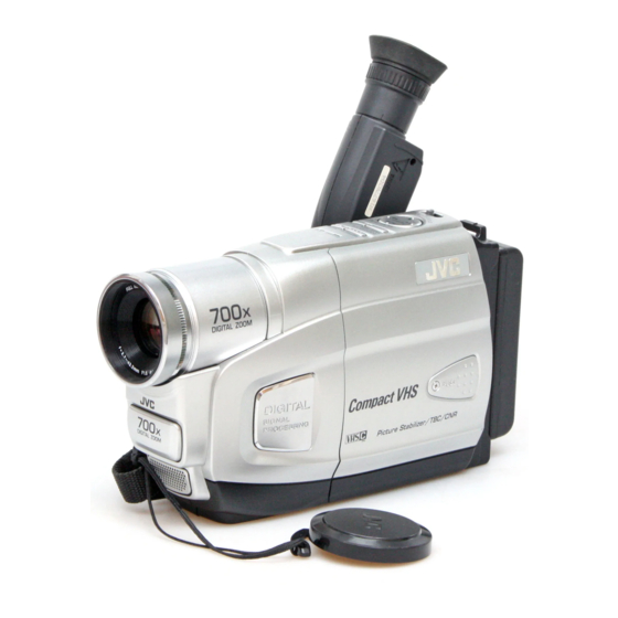
COMPACT VHS CAMCORDER
GR-FX15EK,GR-FX15E
Regarding service information other than these sections, refer to the service manual No. 86712 (GR-SX25EX).
Also, be sure to note important safety precautions provided in the service manual.
SPECIFICATION
(The specifications shown pertain specifically to the model GR-SXM49, FXM393, FXM39, SX25, FX15)
Camcorder
General
Format
: S-VHS (GR-SXM49/SX25 only)/
VHS PAL standard
Power source
: DC 11 V
DC 6 V
Power consumption
Viewfinder on
: 4.2 W (GR-SXM49/FXM393/FXM39 only)
4.0 W (GR-SX25/FX15 only)
LCD monitor* on
: 4.7 W (GR-SXM49/FXM393/FXM39 only)
Video light**
: 3.0 W
* Applicable models only.
** GR-SXM49/FXM393/SX25 only.
Signal system
: PAL-type
Video recording system
Luminance
: FM recording
Colour
: Converted sub-carrier direct recording
Conforms to VHS standard
Cassette
:
Tape speed
SP
: 23.39 mm/sec.
LP
: 11.70 mm/sec.
Recording time (max.)
SP
: 60 minutes
LP
: 120 minutes (with EC-60 cassette)
Operating
temperature
: 0°C to 40°C
Operating humidity
: 35% to 80%
Storage temperature
: -20°C to 50°C
Weight
: Approx. 840 g (GR-SXM49/FXM393/FXM39 only)
Approx. 760 g (GR-SX25 only)
Approx. 750 g (GR-FX15 only)
Dimensions (W x H x D) : 113 mm x 117 mm x 199 mm
(GR-SXM49/FXM393/FXM39 only)
108 mm x 117 mm x 199 mm (GR-SX25/FX15 only)
(with the LCD monitor* closed and with the
viewfinder fully tilted downward)
* Applicable models only.
(Using AC Adapter)
(Using battery pack)
/
cassette
,GR-FX15E
X
: 1/6" format CCD
Pickup
Lens
: F1.6, f = 2.7 mm to 43.2 mm,
16:1 power zoom lens with auto iris and
macro control, filter diameter 40.5 mm
Viewfinder
: Electronic viewfinder with 0.5"
black/white CRT White balance
White balance
: Auto/Manual adjustment
adjustment
Speaker
: Monaural
(Applicable models only)
LCD monitor
: 2.5" diagonally measured, LCD panel/
(Applicable models only)
TFT active matrix system
Connectors
:
Video
1 V (p-p), 75
(via Video output connector)
:
Audio
300 mV (rms), 1 k
(via Audio output connector)
:
S-Video
Y: 1 V (p-p), 75
(GR-SXM49/SX25 only)
C: 0.30 V (p-p), 75
AC Adapter
:
Power requirement
AC 110 V - 240 V ~, 50 Hz/60 Hz
:
Output
DC 11 V
Optional Accessories
• Battery Packs BN-V12U, BN-V20U, BN-V400U
• Compact S-VHS (
) Cassettes SE-C45/30
• Compact VHS (
) Cassettes EC-60/45/30
• Active Carrying Bag CB-V7U
• Cassette Adapter C-P7U
Some accessories are not available in some areas. Please consult your
nearest JVC dealer for details on accessories and their availability.
GR-FX15EK,GR-FX15EX,GR-FX15EY,GR-FX15EZ M3A6B2
,GR-FX15E
Y
unbalanced, analogue output
, analogue output
, analogue output
, analogue output
, 1 A
No. 86718
2003/02
Z
Advertisement
Table of Contents

Related Manuals for JVC GR-FX15EK


Summary of Contents for JVC GR-FX15EK
- Page 1 (with the LCD monitor* closed and with the Some accessories are not available in some areas. Please consult your viewfinder fully tilted downward) nearest JVC dealer for details on accessories and their availability. * Applicable models only. GR-FX15EK,GR-FX15EX,GR-FX15EY,GR-FX15EZ M3A6B2 No. 86718...
-
Page 2: Different Table .................................................................................................................................................................................... 1 To
TABLE OF CONTENTS DIFFERENT TABLE ....................................1 to 2 PARTS LIST 1. PACKING AND ACCESSORY ASSEMBLY <M1> ............................. 3-1 The following table indicate main different points between models GR-SX25EX ,GR-FX15EK ,GR-FX15EX ,GR-FX15EY and GR-FX15EZ. MODEL GR-SX25EX GR-FX15EK GR-FX15EX GR-FX15EY GR-FX15EZ... - Page 3 FINAL ASSEMBLY <M2> REF. MODEL GR-SX25EX GR-FX15EK GR-FX15EX GR-FX15EY GR-FX15EZ ITEM C.COVER(S)ASSY LY20928-001D LY20928-007E LY20928-006E 101F STICKER(C) LY44007-001A — LY44007-001A 101H STICKER(B) LY43982-001A LY43982-005A LOWER CASE ASSY LY20925-002C LY20925-006E F.COVER ASSY LY20926-001C LY20926-003D 135D STICKER(A) LY43983-001A LY43983-002A 135E CAUTION LABEL LY44141-001A —...
- Page 4 Replace only with specified part numbers. 1. PACKING AND ACCESSORY ASSEMBLY <M1> The instruction manual to be provided with this product will differ according to the destination. FINAL ASSEMBLY <M2> MODEL MARK GR-FX15EK GR-FX15EX GR-FX15EY GR-FX15EZ LABEL (SERIAL) <...
- Page 5 (with the LCD monitor* closed and with the Some accessories are not available in some areas. Please consult your viewfinder fully tilted downward) nearest JVC dealer for details on accessories and their availability. * Applicable models only. GR-SX25EK, GR-SX25EX, GR-SX25EZ, GR-SXM49EK, GR-SXM49EX, GR-SXM49EZ M3C7B3,M3C723 No.86712...
-
Page 6: Table Of Contents
TABLE OF CONTENTS Instructions PRECAUTIONS................. . . SAFTY PRECAUTIONS . - Page 7 1.1.2 Safety Check after Servicing Examine the area surrounding the repaired location for damage (4) Leakage current test or deterioration. Observe that screws, parts and wires have been Confirm specified or lower leakage current between earth returned to original positions, Afterwards, perform the following ground/power cord plug prongs and externally exposed ac- tests and confirm the specified values in order to verify compli- cessible parts (RF terminals, antenna terminals, video and...
-
Page 8: Precautions
SECTION 2 SPECIFIC SERVICE INSTRUCTIONS 2.1 BEFORE ASSEMBLY AND DISASSEMBLY 2.1.1 Precautions 2.1.4 Disconnection of connectors (Wires) 1. Be sure to disconnect the power supply unit prior to mount- Pull both ends of the connector in the arrow direction, remove the ing and soldering of parts. -
Page 9: Assembly And Disassembly Of Cabinet Parts
2.2 ASSEMBLY AND DISASSEMBLY OF CABINET PARTS 2.2.1 Disassembly flow chart 2.2.2 Disassembly method This flowchart indicates the disassembly step for the cabinet STEP Fig. parts and board assembly in order to gain access to item(s) to be PART POINT NOTE serviced. - Page 10 CN1a CN1b CN1c (S1) 9 (S2) 10 (S2) 11 (S2) (S1) (S1) (S1) (S1) (S1) (S1) (S1) Fig.C1 <SHOOTING MODEL> (S4) <MONITOR MODEL> Fig.C2 (No.86712)1-7...
- Page 11 (S5a) <NOTE 5> <SHOOTING MODEL> (S5a) (S5a) (S5a) (S5a) <MONITOR MODEL> <NOTE 5> (S5a) (S5b) (S5a) (S5a) (S5a) (S5a) (S5a) Fig.C3 <MONITOR MODEL> (S7b) <NOTE 7a> (S7b) (S7a) <NOTE 7c> (S6) DO NOT MAKE FPC (S6) SLACKEN IN THIS PART. <NOTE 7d>...
- Page 12 0.118N m (1.2kgf (S11) (S8) <NOTE 11> <NOTE 8a> [11] OP BLOCK ASSEMBLY (S11) <NOTE 8b> PASS THE WIRE BETWEEN THESE BOSSES. LIGHT WIRE CN8a DO NOT OBSTRUCT THE RECEIVING PART OF SENSOR CN8b BY WIRE . PASS THE WIRE OUTSIDE OF SCREWING SEQUENCE MIC WIRE...
-
Page 13: Assembly And Disassembly Of [2]Op Block Assemblyccd Board Assembly (Camera Section And Board Assembly)
2.3 ASSEMBLY AND DISASSEMBLY OF CAMERA SECTION AND BOARD ASSEMBLY 2.3.1 Disassembly flow chart This flowchart indicates the disassembly step for the cabinet parts and board assembly in order to gain access to item(s) to be serviced. When reassembling, perform the step(s) in reverse or- der. - Page 14 (S4d) (S4c) <NOTE 4> CN1h FRAME ASSEMBLY CN1g C2 J CN1f CN1a SHIELD CASE (MAIN) CN1b CN1j CN1d CN1c (S4c) (S1) CN1e (S1) SHIELD Fig.D1 (S4a) (S4b) Fig.D3 (S2) (S2) <NOTE 3> FRAME ASSEMBLY (S5) (S5) Fig.D2 Fig.D4 (No.86712)1-11...
- Page 15 2.4 ASSEMBLY AND DISASSEMBLY OF [7]MONITOR ASSEMBLY (CABINET PARTS) 2.4.1 Disassembly of MONITOR ASSEMBLY NOTE : Be careful not to soil or scratch the monitor screen through the disassembly/assembly work. (1) While removing the three screws 1 to 3 in numerical order and disengaging the two hooks (L7a and L7b) in alphabet- (S7a) ical order, remove the MONITOR COVER ASSEMBLY.
- Page 16 2.5 ASSEMBLY AND DISASSEMBLY OF [2]OP BLOCK ASSEMBLY CCD BOARD ASSEMBLY (CAMERA SECTION AND BOARD ASSEMBLY) 2.5.1 Precautions 2.5.3 Assembly of CCD BASE ASSEMBLY and CCD (1) Take care in handling the CCD IMAGE SENSOR, OP LPF BOARD ASSEMBLY and lens components when performing maintenance etc., (1) Set the OP LPF to the OP BLOCK ASSEMBLY so that the especially with regard to surface contamination, attached OP side touches the OP BLOCK ASSEMBLY.
-
Page 17: Emergency Display
2.6 EMERGENCY DISPLAY Example (in case of the error number E01): Whenever some abnormal signal is input to the mechacon CPU, an error number (E01, as an example) is displayed in the elec- tronic view finder. In every error status, such the message as UNIT IN REMOVE AND shown below alternately appear over and over. - Page 18 2.7.1 Operation procedure 2.7.2 Flow chart NOTE: 1. Set the Power Switch to turn on TO S When demonstration is performed, some of the following func- the "M". EXPOSURE AUTO M. W. B . AUTO tions that a model does not have are omitted. Press the MENU Wheel once.
-
Page 19: Take Out Cassette Tape
2.8 TAKE OUT CASSETTE TAPE In the event that the set enters the emergency mode as it is (4) While holding down the cassette housing by hand, con- loaded with a cassette tape and the cassette tape cannot be nect the jumper wires to a battery to run the mechanism ejected with the EJECT button, manually, take it out of the set to the EJECT position four unloading. -
Page 20: Service Note
2.9 SERVICE NOTE Use the following chart to manage screws (No.86712)1-17... -
Page 21: Adjustment
MENT WITH PERSONAL COMPUTER is setup and it ad- PUJ50431-2 PTU94002-2 justs using a service support system. Please contact to JVC Service for detail information. • OP BLOCK • EEP ROM (IC102 of MAIN board) • MONITOR In the event of malfunction with electrical circuits, trouble- shooting with the aid of proper test instruments most be Conn. - Page 22 1,2. Alignment tape 10.Light box assembly To be used for check and adjustment of interchangeability of To be used for adjustment of the camera system. For the us- the mechanism. age of the Light box assembly, refer to the Service Bulletin No. (Video: Color bar signal, Audio: Non-signal) YA-SB-10035.
-
Page 23: Mechanism Adjustment
3.3 MECHANISM ADJUSTMENT 3.3.1 TAPE TRANSPORT ADJUSTMENT Mechanism adjustment is needed when DRUM ASSEMBLY or a BACK TENSION part of the tape transport system is replaced. To protect tapes 0.97x10 - 1.71x10 • from damage, first clean the tape transport system, next confirm PLAY TORQUE (10-17gf·cm) 1.47x10... - Page 24 NOTE: 3.3.4 A/C head height & azimuth To prevent the tape from damage, turn the guide rollers Remove the exterior parts attached to the UPPER CASE slowly. ASSEMBLY so that the screws around the A/C HEAD (7) By operating the tracking button (both in + and - directions) ASSEMBLY can be tighten or loosen.
- Page 25 3.3.5 Phase of control head (X value) Note: Remove the exterior parts attached to the UPPER CASE ASSEMBLY so that the screws around the A/C HEAD ASSEMBLY can be tighten or loosen. (1) Connect the JIG CONNECTOR CABLE to CN25 on the MAIN BOARD ASSEMBLY.
-
Page 26: Electrical Adjustment
3.4 ELECTRICAL ADJUSTMENT 3.4.1 ELECTRICAL ADJUSTMENT WITH PERSONAL COMPUTER • Electrical adjustment except for B/W VF ASSEMBLY is per- • Remove the COVER (JIG) to perform adjustment. formed by using PERSONAL COMPUTER. As for the cable NOTE: connection, see Fig. 3-4-1. Read README.TXT file to use the For the connection of the JIG CONNECTOR CABLE, refer to software for SERVICE SUPPORT SYSTEM properly. - Page 27 3.4.2 B/W VF ASSEMBLY (E. VF) ADJUSTMENT Referring to “SEC. 2 SPECIFIC SERVICE INSTRUCTIONS” and 3.4.2.1 Tilt connect the E. VF WIRE to CN12 of the MAIN BOARD Subject • Alignment tape ASSEMBLY. • Stairstep Mode • PB (LY20701) Equipment •...
- Page 28 (with the LCD monitor* closed and with the Some accessories are not available in some areas. Please consult your viewfinder fully tilted downward) nearest JVC dealer for details on accessories and their availability. * Applicable models only. GR-SX25EK, GR-SX25EX, GR-SX25EZ, GR-SXM49EK, GR-SXM49EX, GR-SXM49EZ M3C7B3,M3C723 No.86712SCH...
-
Page 29: Board Interconnections
BOARD INTERCONNECTIONS NOTES : The number of patch cords are indicated by interconnected. LCD_MODULE CN7602 (Page 2-15) BL_GND (Page 2-14) (Page 2-16) CN7601 YTU94074-14 YTU93082G YTU94077-14 CN5301 YUJ40095A-3 YTU94074-22 YTU94077-22 CN25 CN16 CN12 CN22 CN15 VDDSC PBLK PBLK AD_0 AD_0 AD_1 AD_1 AD_2... -
Page 30: Cpu Schematic Diagram
CPU SCHEMATIC DIAGRAM NOTES : For the destination of each signal and further line connections that are cut off from this diagram, refer to "BOARD INTERCONNECTIONS". When ordering parts, be sure to order according to the Part Number indicated in the Parts List. 0 1 MAIN(CPU) UNREG R104... -
Page 31: M.mda Schematic Diagram
M.MDA SCHEMATIC DIAGRAM NOTES : For the destination of each signal and further line connections that are cut off from this diagram, refer to "BOARD INTERCONNECTIONS". When ordering parts, be sure to order according to the Part Number indicated in the Parts List. 0 1 MAIN(M.MDA) IC1602 TA75S393F-X... -
Page 32: Asp Schematic Diagram
ASP SCHEMATIC DIAGRAM NOTES : For the destination of each signal and further line connections that are cut off from this diagram, refer to "BOARD INTERCONNECTIONS". When ordering parts, be sure to order according to the Part Number indicated in the Parts List. 0 1 MAIN(ASP) CN25 V_OVL... -
Page 33: Dsp Schematic Diagram
DSP SCHEMATIC DIAGRAM NOTES : For the destination of each signal and further line connections that are cut off from this diagram, refer to "BOARD INTERCONNECTIONS". When ordering parts, be sure to order according to the Part Number indicated in the Parts List. DAC5 0 1 MAIN(DSP) BWYGAIN... -
Page 34: F/Z/I/Mda Schematic Diagram
F/Z/I/MDA SCHEMATIC DIAGRAM NOTES : For the destination of each signal and further line connections that are cut off from this diagram, refer to "BOARD INTERCONNECTIONS". When ordering parts, be sure to order according to the Part Number indicated in the Parts List. 0 1 MAIN(F/Z/I/MDA) IRIS_O/C TO OP BLOCK... -
Page 35: Out Schematic Diagram
V OUT SCHEMATIC DIAGRAM NOTES : For the destination of each signal and further line connections that are cut off from this diagram, refer to "BOARD INTERCONNECTIONS". When ordering parts, be sure to order according to the Part Number indicated in the Parts List. 0 1 MAIN(V OUT) L4701 TO REG... -
Page 36: Tg/Cds Schematic Diagram
TG/CDS SCHEMATIC DIAGRAM NOTES : For the destination of each signal and further line connections that are cut off from this diagram, refer to "BOARD INTERCONNECTIONS". When ordering parts, be sure to order according to the Part Number indicated in the Parts List. L5205 0 1 MAIN(TG/CDS) NQR0129-002X... -
Page 37: Reg Schematic Diagram
REG SCHEMATIC DIAGRAM NOTES : For the destination of each signal and further line connections that are cut off from this diagram, refer to "BOARD INTERCONNECTIONS". When ordering parts, be sure to order according to the Part Number indicated in the Parts List. 0 1 MAIN(REG) CN28 ADP_H... -
Page 38: Lcd Schematic Diagram
LCD SCHEMATIC DIAGRAM NOTES : For the destination of each signal and further line connections that are cut off from this diagram, refer to "BOARD INTERCONNECTIONS". When ordering parts, be sure to order according to the Part Number indicated in the Parts List. 0 1 MAIN(LCD) CN16 OPEN_SW... -
Page 39: Bw/Vf Schematic Diagram
BW/VF SCHEMATIC DIAGRAM NOTES : For the destination of each signal and further line connections that are cut off from this diagram, refer to "BOARD INTERCONNECTIONS". When ordering parts, be sure to order according to the Part Number indicated in the Parts List. 0 1 MAIN(BW/VF) (NC) BWBLEVEL... -
Page 40: Jack Schematic Diagram
JACK SCHEMATIC DIAGRAM NOTES : For the destination of each signal and further line connections that are cut off from this diagram, refer to "BOARD INTERCONNECTIONS". When ordering parts, be sure to order according to the Part Number indicated in the Parts List. CN9031 0 1 MAIN(JACK) R9402... -
Page 41: Speaker Schematic Diagram
SPEAKER SCHEMATIC DIAGRAM CCD SCHEMATIC DIAGRAM NOTES : For the destination of each signal and further line connections that are cut off from NOTES : For the destination of each signal and further line connections that are cut off from this diagram, refer to "BOARD INTERCONNECTIONS". -
Page 42: Monitor Schematic Diagram
MONITOR SCHEMATIC DIAGRAM NOTES : For the destination of each signal and further line connections that are cut off from this diagram, refer to "BOARD INTERCONNECTIONS". When ordering parts, be sure to order according to the Part Number indicated in the Parts List. 0 7 MONITOR J7501 NCB21EK-273X... -
Page 43: Vf Chematic Diagram
E. VF SCHEMATIC DIAGRAM NOTES : For the destination of each signal and further line connections that are cut off from this diagram, refer to "BOARD INTERCONNECTIONS". When ordering parts, be sure to order according to the Part Number indicated in the Parts List. 6 0 E. -
Page 44: Top Ope Unit, Zoom Unit, Rear Unit And Sensor Schematic Diagrams
TOP OPE UNIT, ZOOM UNIT, REAR UNIT AND SENSOR SCHEMATIC DIAGRAMS NOTES : For the destination of each signal and further line connections that are cut off from this diagram, refer to "BOARD INTERCONNECTIONS". The schematic diagram is only for reference. Avoid replacing individual parts. TOP OPE UNIT Replace the entire unit only. -
Page 45: Main Circuit Board
MAIN CIRCUIT BOARD <01>MAIN YB10400-01-02 FOIL SIDE (B) C2003 L9302 C126 L2003 R5219 C9316 C9319 R2001 C4049 C142 R9315 R5215 L9303 IC2001 L2005 C2005 R9316 L4002 C9304 C9305 R2006 R2004 R9306 R5216 R2002 C9324 R9308 R9303 R9307 R5203 R136 R9305 C9315 Q2007 R2012... - Page 46 COMPONENT PARTS LOCATION GUIDE <MAIN> YB10400-01-02 (1/2) REF.NO. LOCATION REF.NO. LOCATION REF.NO. LOCATION REF.NO. LOCATION REF.NO. LOCATION REF.NO. LOCATION REF.NO. LOCATION REF.NO. LOCATION REF.NO. LOCATION REF.NO. LOCATION REF.NO CAPACITOR C2023 C4049 B C 4D C6010 B C 2C C9322 B C 4C IC4201 Q2021 R123...
- Page 47 COMPONENT PARTS LOCATION GUIDE <MAIN> YB10400-01-02 (2/2) REF.NO. LOCATION REF.NO. LOCATION REF.NO. LOCATION REF.NO. LOCATION REF.NO. LOCATION REF.NO. LOCATION REF.NO. LOCATION REF.NO. LOCATION REF.NO. LOCATION REF.NO. LOCATION REF. R6024 R7313 TL9004 R6025 B C 2C R9102 A C 4C TL9005 R6026 B C 2C R9104...
-
Page 48: Main Circuit Board
MAIN CIRCUIT BOARD <01>MAIN YB10400-01-02 COMPONENT SIDE (A) ZP-CCD1 ZP-CCD2 R7313 IC103 R9104 R9102 ZP33-16 ZP33-14 R7312 Q9101 Q9103 CN22 F7301 C5223 C125 CN9013 R7311 CN9012 Q9102 Q9104 CN13 ZP101-1 R156 R7310 C1630 ZP13-11 C5216 C107 ZP12-3 RA9101 TL9006 R154 IC5202 Q7302 C111... -
Page 49: Monitor Circuit Board
MONITOR CIRCUIT BOARD <07>MONITOR YB20935 FOIL SIDE (B) COMPONENT PARTS LOCATION GUIDE <07>MONITOR YB20935 COMPONENT SIDE (A) <MONITOR> YB20935 REF.NO. LOCATION REF.NO. LOCATION REF.NO. LOCATION CAPACITOR R7639 C7501 TRANSISTOR R7640 C7502 Q7501 R7641 C7503 Q7502 R7642 C7504 Q7503 R7643 C7601 Q7504 R7644 C7602... -
Page 50: Ccd Circuit Board
CCD CIRCUIT BOARD WAVEFORMS — ASP — <02>CCD YB10400-01-02 IC3501-19 IC3501-20 IC3501-21 IC3501-25 FOIL SIDE (B) COMPONENT SIDE (A) REC 0.11 Vp-p REC 0.35 Vp-p 24 mVp-p 0.26 Vp-p 2 mV/10 µsec/DIV 10 mV/10 µsec/DIV 1 mV/5 msec/DIV 10 mV/5 msec/DIV —... -
Page 51: Voltage Charts
VOLTAGE CHARTS <CPU> <M.MDA> <ASP> <DSP> <F/Z/I/MDA> <V-OUT> <TG CDS> <REG> MODE MODE MODE MODE MODE MODE MODE MODE MODE MODE MODE MODE MODE MODE MODE MODE PLAY PLAY PLAY PLAY PLAY PLAY PLAY PLAY PLAY PLAY PLAY PLAY PLAY PLAY PLAY PIN NO. -
Page 52: Power System Block Diagram
POWER SYSTEM BLOCK DIAGRAM REAR UNIT MAIN REG SECTION M. MDA SECTION DRM_PWR Q6401 L6002 F6008 UNREG DRM_PWR DRUM POWER L6001 CAP_PWR F6001 CN28 DRM_CTL BATT_+ CAP_PWR BATT_+ IC6001-6,39PIN Q6501 M_UNREG REG_3.2V ADP_DC POWER CAPSTAN ADP_DC F6002 M_UNREG ADP_H MOTOR ADP_H CAP_CTL CAPMR_BS... -
Page 53: Cpu/Mda System Block Diagram
CPU/M.MDA SYSTEM BLOCK DIAGRAM MAIN (CPU) (M. MDA) IC101(CPU) IC1601 DRUM ROTOR POSI POSITION CENTER IC103 RTC CS (RTC) AL SI START UP TIMMING SWITCHING DRUM CLK CONTROL CONTROL SCLK AL CLK D COIL U OSCIN D COIL U FORWARD DRUM ON C1617 C1619... -
Page 54: Monitor System Block Diagram
MONITOR SYSTEM BLOCK DIAGRAM LCD MONITOR T7501 T7501 MONITOR FROM REG CN16 CN7601 F7501 F7501 REG_4.8V REG_4.8V REG_4.8V Q7503 Q7503 Q7501 Q7501 Q7504 Q7504 Q7502 Q7502 FROM CPU LCD_CTL CN7602 L7604 LCD_CTL REG_15V L7601 REG_3.2V MREG_4.8V VSS(REG_-15V) REG_3.2V CLK1 CLK1 IC7602 R7607 L7605... -
Page 55: Camera And Y/C System Block Diagram
CAMERA AND Y/C SYSTEM BLOCK DIAGRAM (1/2) 0 2 CCD MAIN V_PB_C IC5201 (TG/CDS) IC4001(DSP) (DSP) (CDS/AGC/AD/TG) IC5301 Q5301 CN5301 CN22 CCD_OUT CDSIN γ BLKSH PROCESS OP BLOCK CONV CLAMP γ T. G SEPA DSP CONTROL BLKFB (3LINE) OFFSET CDS_CLK INTER FACE ADCLK SERIAL INTERFACE... - Page 56 CAMERA AND Y/C SYSTEM BLOCK DIAGRAM (2/2) JIG_CONN. CN25 J504 A/V OUT V_PB_C IC4001(DSP) J505 S OUT IC4701 DA_R (V OUT) ∗ DA_B IC4702 Y/C MIX TO LCD/CVF &6dB AMP (V OUT) Q3502 IC3501 CH2_S DA_G (ASP) PB AMP TO BW/CVF CH2_F BWY0 BWYOUT...
-
Page 57: Parts List
PARTS LIST SAFETY PRECAUTION Parts identified by the symbol are critical for safety. Replace only with specified part numbers. 1. PACKING AND ACCESSORY ASSY <M1> The instruction manual to be provided with this product will differ according to the destination. FINAL ASSEMBLY <M2>... - Page 58 2. FINAL ASSY <M2> BEWARE OF BOGUS PARTS Parts that do not meet specifications may cause trouble in regard to safety and performance. We recommend that genuine JVC parts be used. ELECTRONIC VIEWFINDER ASSEMBLY <M4> MAIN BOARD ASSEMBLY <01> 121B...
- Page 59 145A 145B 145E OARD MBLY > 145D 145G 145C MECHANISM 145D ASSEMBLY <M3> 145F 145F F7 F4 145D 145D 154A R MODEL RATING 261B LABEL MONITOR MODEL 261A 101E 101F 101C 101A NOTE: 101D There are two types of FRONT FRAME 101G 101E MONITOR...
-
Page 60: Final Assembly
FINAL ASSEMBLY <M2> Symbol No. Part No. Part Name Description Local Symbol No. Part No. Part Name Description Local LY32953-001A C.COVER INSIDE LY10392-001C TOP OPE UNIT LY20928-003D C.COVER(S) ASSY LY20952-001C REAR BOARD ASSY LY20928-001D C.COVER(S) ASSY QYSLSF2060D TAP SCREW 2mm x 6mm(x2) LY20927-001C C.COVER(M) ASSY... - Page 61 3. MECHANISM ASSEMBLY <M3> BEWARE OF BOGUS PARTS Parts that do not meet specifications may cause trouble in regard to safety and performance. We recommend that genuine JVC parts be used. 469A 469B 469B 439A 429A 406B 406A Classification Part No.
-
Page 62: Mechanism Assembly
Symbol No. Part No. Part Name Description Local LY42754-003A SLIT WASHER LY42571-001A TENSION ARM ASSY 439A LY42669-001A TENSION SPRING LY42754-003A SLIT WASHER YQ20797-1-5 MOTOR BASE LY42722-001A SCREW (x2) YQ44460 SCREW QAR0212-002 CAPSTAN MOTOR YQ44304 TAPPING SCREW (x3) LY42731-001A SLANT POLE BASE ASSY YQ44304 TAPPING SCREW YQ43710-2... -
Page 63: Electronic Viewfinder Assembly
4. ELECTRONIC VIEWFINDER ASSEMBLY <M4> E.VF BOARD ASSEMBLY <60> 357A SERIAL NO. LABEL Symbol No. Part No. Part Name Description Local ELECTRONIC VIEWFINDER ASSY<M4> Symbol No. Part No. Part Name Description Local 356 PTY20701-011 BOTTOM CASE ASSY PTY20374-201 LENS ASSY 357A... -
Page 64: Monitor Assembly
5. MONITOR ASSEMBLY <M5> [D, E, F] MONITOR ASSEMBLY <M5> Symbol No. Part No. Part Name Description Local LY20947-001A MONITOR ASSY 501A LY33066-001A M.COVER ASSY 501A LY43982-001A STICKER(B) LY33077-001B M.CASE ASSY 502A LY32967-001B KNOB(LOCK) 502B LY32988-001A LOCK SPRING 502C QYSLSF2050Z TAP SCREW 2mm x 5mm... -
Page 65: Electrical Parts List
6. ELECTRICAL PARTS LIST MAIN BOARD ASSEMBLY <01> Symbol No. Part No. Part Name Description Local Symbol No. Part No. Part Name Description Local Q2401 or RN1104-X DIGI TRANSISTOR D,E,F Q2401 or BCR148T-X DIGI TRANSISTOR D,E,F YB10400EB1-02 MAIN BOARD ASSY A,B,C Q3501 HN1C01FU/G/-X... - Page 66 Symbol No. Part No. Part Name Description Local Symbol No. Part No. Part Name Description Local D6701 CRS09-X SB DIODE C2033 NBE20JM-475X TA E CAPACITOR 4.7uF 6.3V M D6702 CRS09-X SB DIODE C2034 NCB31CK-104X C CAPACITOR 0.1uF 16V K C2035 NBE20JM-226X TA E CAPACITOR...
- Page 67 Symbol No. Part No. Part Name Description Local Symbol No. Part No. Part Name Description Local C4252 NCB31CK-104X C CAPACITOR 0.1uF 16V K C6302 NCB10JK-106X C CAPACITOR 10uF 6.3V K C4253 NCB31EK-153X C CAPACITOR 0.015uF 25V K C6303 NBE40JM-476X TA E CAPACITOR 47uF 6.3V M...
- Page 68 Symbol No. Part No. Part Name Description Local Symbol No. Part No. Part Name Description Local R148 NRSA63J-222X MG RESISTOR 2.2kΩ 1/16W J R2072 NRSA63J-103X MG RESISTOR 10kΩ 1/16W J R149 NRSA63J-222X MG RESISTOR 2.2kΩ 1/16W J R2401 NRSA63J-392X MG RESISTOR 3.9kΩ...
- Page 69 Symbol No. Part No. Part Name Description Local Symbol No. Part No. Part Name Description Local R4509 NRSA63J-182X MG RESISTOR 1.8kΩ 1/16W J R7004 NRSA63D-123X MG RESISTOR 12kΩ 1/16W D D,E,F R4516 NRSA63J-271X MG RESISTOR 270Ω 1/16W J R7005 NRSA63J-223X MG RESISTOR...
-
Page 70: Ccd Board Assembly <02
Symbol No. Part No. Part Name Description Local Symbol No. Part No. Part Name Description Local QGF0507F3-11X CONNECTOR FFC/FPC (1-11) Q7504 or UN9213J-X DIGI TRANSISTOR QGA1201C2-02X CONNECTOR W-B (1-2) Q7504 or RN1104-X DIGI TRANSISTOR QGF0507F3-11X CONNECTOR FFC/FPC (1-11) Q7504 or BCR148T-X DIGI TRANSISTOR QGA1201C2-02X... -
Page 71: E.vf Board Assembly <60
Symbol No. Part No. Part Name Description Local Symbol No. Part No. Part Name Description Local R7618 NRSA63J-0R0X MG RESISTOR 0Ω 1/16W J C7003 QEDP1AM-227 E CAPACITOR 220uF 10V M R7621 NRSA63J-102X MG RESISTOR 1kΩ 1/16W J C7004 QEDP1AM-227 E CAPACITOR 220uF 10V M...