Table of Contents
Advertisement
SERVICE MANUAL
Ver. 1.2 2012.06
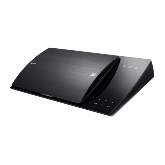
• HBD-N590 is the Blu-ray disc
• HBD-N790W is the Blu-ray disc
• HBD-N890W is the Blu-ray disc
• HBD-N990W is the Blu-ray disc
• HBD-N995W is the Blu-ray disc
• HBD-T79 is the Blu-ray disc
TM
• In order to perform the operation checking, all the units contained in this unit are needed.
Amplifier Section
HBD-N790W/N890W/N990W/N995W/T79
U.S.models:
AUDIO POWER SPECIFICATIONS
POWER OUTPUT AND TOTAL HARMONIC
DISTORTION:
(FTC)
Front L + Front R:
With 3 ohms loads, both
channels driven, from 180
Hz - 20 kHz; rated 50 watts
per channel minimum
RMS power, with no more
than 1% total harmonic
distortion from 250 milli
watts to rated output.
Except US and Chinese models:
POWER OUTPUT (rated)
Front L/Front R:
78 W + 78 W (at 3 ohms, 1
kHz, 1% THD)
POWER OUTPUT (reference) (Except Chinese model)
Front L/Front R:
125 W (per channel at
3 ohms, 1 kHz)
Center:
250 W (at 6 ohms, 1 kHz)
Subwoofer:
250 W (at 6 ohms, 80 Hz)
POWER OUTPUT (reference) (Chinese model)
Front L/Front R:
75 W (per channel at
3 ohms, 1 kHz)
Center:
150 W (at 6 ohms, 1 kHz)
Subwoofer:
150 W (at 6 ohms, 80 Hz)
Inputs (Analog)
AUDIO (AUDIO IN)
Sensitivity: 3.0 V/1.0 V
Inputs (Digital)
TV (Audio Return Channel/OPTICAL)
Supported formats: LPCM
2CH (up to 48 kHz), Dolby
Digital, DTS
9-893-438-03
Sony Corporation
2012F33-1
©
2012.06
Published by Sony Techno Create Corporation
HBD-N590/N790W/N890W/
Photo: HBD-N990W
/DVD receiver in BDV-N590.
TM
/DVD receiver in BDV-N790W.
TM
/DVD receiver in BDV-N890W.
TM
/DVD receiver in BDV-N990W.
TM
/DVD receiver in BDV-N995W.
TM
/DVD receiver in BDV-T79.
SPECIFICATIONS
HDMI (IN 1)/HDMI (IN 2)
Supported formats: LPCM
5.1CH (up to 48 kHz),
LPCM 2CH (up to
96 kHz), Dolby Digital,
DTS
HBD-N590
POWER OUTPUT (rated)
Front L/Front R:
78 W + 78 W (at 3 ohms,
1 kHz, 1% THD)
POWER OUTPUT (reference)
Front L/Front R/Surround L/Surround R:
125 W (per channel at
3 ohms, 1 kHz)
Center:
250 W (at 6 ohms, 1 kHz)
Subwoofer:
250 W (at 6 ohms, 80 Hz)
Inputs (Analog)
AUDIO (AUDIO IN)
Sensitivity: 3.0 V/1.0 V
Inputs (Digital)
TV (Audio Return Channel/OPTICAL)
Supported formats: LPCM
2CH (up to 48 kHz), Dolby
Digital, DTS
HDMI (IN 1)/HDMI (IN 2)
Supported formats: LPCM
5.1CH (up to 48 kHz),
LPCM 2CH (up to
96 kHz), Dolby Digital,
DTS
Video Section
Outputs
VIDEO: 1 Vp-p 75 ohms
HDMI Section
Connector
Type A (19pin)
BD/DVD/Super Audio CD/CD System
Signal format system
US, Canadian and PX models:
NTSC
AEP model: PAL
Other models: NTSC/PAL
N990W/N995W/T79
Saudi Arabia Model
Middle East Model
HBD-N590/N790W/N890W/N990W
Model Name Using Similar Mechanism
Mechanism Type
Optical Pick-up Name
USB Section
USB 1/2 port:
Type A (For connecting
USB memory, memory
card reader, digital still
camera, and digital video
camera)
LAN Section
LAN (100) terminal
100BASE-TX Terminal
Wireless LAN Section
Standards Compliance
IEEE 802.11 b/g/n
Frequency and Channel
2.4 GHz - 2.4835 GHz
[CH1 -11]
(US and Canadian models)
[CH1 -13]
(Except US and Canadian models)
FM Tuner Section
System
PLL quartz-locked digital
synthesizer
Tuning range
87.5 MHz - 108.0 MHz
(50 kHz step)
(Except US, Canadian and PX
models)
87.5 MHz - 108.0 MHz
(100 kHz step)
(US, Canadian and PX models)
Antenna (aerial)
FM wire antenna (aerial)
Antenna (aerial) terminals 75 ohms, unbalanced
BLU-RAY DISC
US Model
HBD-N790W/N890W/T79
Canadian Model
Russian Model
Iranian Model
Taiwan Model
HBD-N890W/N990W
AEP Model
UK Model
HBD-N590/N790W
Australian Model
HBD-N590/N990W
Chinese Model
HBD-N995W
PX Model
HBD-N790W
Mexican Model
Thai Model
Indian Model
HBD-N990W
Singapore Model
HBD-N590/N890W/N990W
NEW
BSX-3
KEM-480AAA
General
Power requirements
120 V AC, 60 Hz
(US and Canadian models)
120 V AC, 50/60 Hz
(Taiwan model)
110 V - 240 V AC,
50/60 Hz (Mexican and PX models)
220 V - 240 V AC,
50/60 Hz
(Except US, Canadian, Mexican,
Taiwan and PX models)
Power consumption
HBD-N995W
On: 110 W
Standby: 0.3 W (at the
Power Saving mode)
HBD-N790W/N890W/N990W/T79
On: 115 W
Standby: 0.3 W (at the
Power Saving mode)
HBD-N590
On: 135 W
Standby: 0.3 W (at the
Power Saving mode)
– Continued on next page –
/DVD RECEIVER
TM
Advertisement
Table of Contents

Related Manuals for Sony HBD-N590


Summary of Contents for Sony HBD-N590
-
Page 1: Specifications
Chinese Model HBD-N995W PX Model Photo: HBD-N990W HBD-N790W Mexican Model • HBD-N590 is the Blu-ray disc /DVD receiver in BDV-N590. Thai Model • HBD-N790W is the Blu-ray disc /DVD receiver in BDV-N790W. Indian Model • HBD-N890W is the Blu-ray disc /DVD receiver in BDV-N890W. - Page 2 LES DIAGRAMMES SCHÉMATIQUES ET LA LISTE DES and/or other countries. rights reserved. PIÈCES SONT CRITIQUES POUR LA SÉCURITÉ DE FONC- TIONNEMENT. NE REMPLACER CES COMPOSANTS QUE PAR DES PIÈCES SONY DONT LES NUMÉROS SONT DON- ® ® Wi-Fi , Wi-Fi Protected Access NÉS DANS CE MANUEL OU DANS LES SUPPLÉMENTS...
-
Page 3: Table Of Contents
HBD-N590/N790W/N890W/N990W/N995W/T79 Ver. 1.1 TABLE OF CONTENTS SERVICING NOTES ..........5-6. Schematic Diagram - MB-149 Board (1/11) - ....43 5-7. Schematic Diagram - MB-149 Board (2/11) - ....44 DISASSEMBLY 5-8. Schematic Diagram - MB-149 Board (3/11) - ....45 2-1. -
Page 4: Servicing Notes
HBD-N590/N790W/N890W/N990W/N995W/T79 SECTION 1 SERVICING NOTES NOTE OF REPLACING THE IC101 AND IC501 ON NOTES ON HANDLING THE OPTICAL PICK-UP THE MB-149 BOARD BLOCK OR BASE UNIT IC101 and IC501 on the MB-149 board cannot exchange with single. When these parts are damaged, exchange the complete The laser diode in the optical pick-up block may suffer electro- mounted board. - Page 5 HBD-N590/N790W/N890W/N990W/N995W/T79 NOTE OF REPLACING THE OPTICAL DEVICE (KEM- 1-3. Barcode decoder (BDPRdec) 480AAA) OR MB-149 BOARD Jig name: BDPRdec.exe Software contents: The password will be supplied to only service HQ, and • BDPRdec.exe : Barcode decoder software service center name, q’ty and all of software registered •...
- Page 6 HBD-N590/N790W/N890W/N990W/N995W/T79 2. Pass-fail judgment of the optical device (KEM-480AAA) Perform pass-fail judgment to judge whether the repair of the optical device (KEM-480AAA) is necessary. 2-1. Flow of drive section check Confirm whether the Confirm F5303, Confirm whether drive voltage is the...
- Page 7 HBD-N590/N790W/N890W/N990W/N995W/T79 3. Optical device (KEM-480AAA) replacement Flow of replacement: Note: The photo in fl ow is an image. Save the text data to USB memory Barcode label on (memory capacity new optical device need not be 8GB) (KEM-480AAA) bottom side...
- Page 8 – NX_AMP Board (Component Side) – The written example of model number label Displayed characters/values are example. IC3302 IC3102 Part No. Part No. Model Part No. HBD-N590: AEP 4-409-290-0[] HBD-N590: UK 4-409-290-1[] HBD-N790W: US 4-409-291-0[] HBD-N790W: AEP 4-409-292-0[] HBD-N790W: UK...
- Page 9 ADVANCE PREPARATION WHEN CONFIRMING OP- CHECKING METHOD OF NETWORK OPERATION ERATION (HBD-N590/N790W/N890W/N990W/T79 only) In order to perform the operation checking, all the units contained It is necessary to check the network operation, when replacing the in this unit are needed.
- Page 10 HBD-N590/N790W/N890W/N990W/N995W/T79 Ver. 1.1 INSTALLATION METHOD OF THE WIRELESS SOUND SYSTEM (HBD-N790W/N890W/N990W/N995W/T79 only) Procedure: 1. Insert the wireless transceiver (EZW-RT50 (HBD-N790W/ N890W/N990W/T79) or EZW-RT20 (HBD-N995W)) of the attachment in the wireless transceiver slot in the back of the main unit (HBD-N790W/N890W/N990W/N995W/T79) and the surround amplifi...
- Page 11 HBD-N590/N790W/N890W/N990W/N995W/T79 HOW TO EJECT THE DISC WHEN POWER SWITCH TURN OFF The BD drive is taken out, and please rotate the pulley in the direction of the arrow by screwdriver etc. after detaching and take out the disc. disc – BD drive bottom view –...
-
Page 12: Disassembly
HBD-N590/N790W/N890W/N990W/N995W/T79 Ver. 1.1 SECTION 2 DISASSEMBLY • This set can be disassembled in the order shown below. 2-1. DISASSEMBLY FLOW 2-2. COVER (TOP) BLOCK (Page 13) 2-3. TOUCH BOARD 2-4. COVER (BOTTOM) BLOCK 2-5. SHIELD (DRIVE) (Page 14) (Page 15) (Page 16) 2-6. -
Page 13: Cover (Top) Block
HBD-N590/N790W/N890W/N990W/N995W/T79 Note: Follow the disassembly procedure in the numerical order given. 2-2. COVER (TOP) BLOCK 1 two screws (BV DIA. 2.6 1 five screws (BV DIA. 2.6 – Rear bottom view – Note 1: Please spread a sheet under a unit not to injure cover (top). -
Page 14: Touch Board
HBD-N590/N790W/N890W/N990W/N995W/T79 2-3. TOUCH BOARD Note 1: When TOUCH board is defective, exchange the complete mounted board. 3 reflector (touch) assy 1 connector (CN701) 4 TOUCH board Note 3: Since it is pasted by adhesion sheet, remove carefully. Note 2: Please spread a sheet under a unit not to injure cover (top). -
Page 15: Cover (Bottom) Block
HBD-N590/N790W/N890W/N990W/N995W/T79 Ver. 1.1 2-4. COVER (BOTTOM) BLOCK 1 three screws (BV DIA. 2.6 1 three screws 1 two screws (BV DIA. 2.6 (BV DIA. 2.6 – Rear bottom view – 4 chassis (main) block 3 Remove the chassis (main) block in the direction of an arrow. -
Page 16: Shield (Drive)
HBD-N590/N790W/N890W/N990W/N995W/T79 2-5. SHIELD (DRIVE) 1 two screws 1 two screws (BV3) (BV3) 2 shield (drive) 2-6. BD DRIVE (BSX-3) 9 BD drive (BSX-3) 1 two screws Note: When installing the wire (flat type), (BV3) 1 two screws ensure the coloured line. -
Page 17: Led Board
HBD-N590/N790W/N890W/N990W/N995W/T79 Ver. 1.1 2-7. LED BOARD 1 screw (BV3) 3 cover (indicator) block 2 claw 6 LED board 5 connector (CN330) 4 Remove the LED board in the direction of an arrow. 2-8. WIRELESS LAN CARD (WLC1) (EXCEPT N995W) Note: When the wireless LAN card (WLC1) is replaced, refer to “CHECKING METHOD OF NETWORK OPERATION”... -
Page 18: Chassis (Middle) Block
HBD-N590/N790W/N890W/N990W/N995W/T79 2-9. CHASSIS (MIDDLE) BLOCK 2 wire (flat type) (11 core) 1 tape (CN6303) Note: When installing the wire (flat type), 5 two screws ensure the coloured line. (BV3) 5 two screws No slanting after insertion. (BV3) wire (flat type) -
Page 19: Ws Board Block (Except N590)
HBD-N590/N790W/N890W/N990W/N995W/T79 2-11. WS BOARD BLOCK (EXCEPT N590) 2 two screws (BV3) Note: When installing the wire (flat type), 3 WS board block ensure the coloured line. No slanting after insertion. wire (flat type) coloured line 1 wire (flat type) (13 core) -
Page 20: Switching Regulator (Swr1)
HBD-N590/N790W/N890W/N990W/N995W/T79 2-13. SWITCHING REGULATOR (SWR1) 1 power cord connector (CN1) 5 two screws (BV3) 5 two screws (BV3) 6 switching regulator (SWR1) 5 screw (BV3) 3 connector (CN4) 2 connector (CN101) 4 connector (CN301) Switching regulator (SWR1) setting switching regulator (SWR1) -
Page 21: Bracket (Ps)
HBD-N590/N790W/N890W/N990W/N995W/T79 2-14. BRACKET (PS) 2 insulator (bottom) 1 two screws (B3) 4 screw (B3) Wire e i 5 bracket (PS) 4 screw (B3) 3 two screws (B3) bracket (PS) 2-15. POWER CORD (AC1) 1 two claws Cord bushing (FBS001) setting... -
Page 22: Heat Sink (Amp)
HBD-N590/N790W/N890W/N990W/N995W/T79 2-16. HEAT SINK (AMP) 2 three screws (transistor) 3 heat sink (AMP) Wire setting clamp NX_AMP board 1 Remove wire from the clamp. heat sink (AMP) SAFETY STANDARD 2-17. NX_AMP BOARD Note 1: When the NX_AMP board is replaced, spread the compound referring to “NOTE OF REPLACING THE IC3102 AND... -
Page 23: Board
HBD-N590/N790W/N890W/N990W/N995W/T79 Ver. 1.1 2-18. MB-149 BOARD Note 1: When the MB-149 board is replaced, refer to “CHECKING METHOD OF NETWORK OPERATION” on servicing notes (page 9). 1 connector (CN5301) 2 wire (flat type) (22 core) (CN5905) (EXCEPT N590)/ (24 core) (CN5904) (N590) -
Page 24: Bottom Cover
HBD-N590/N790W/N890W/N990W/N995W/T79 2-19. BOTTOM COVER 2 wire (flat type) (7 core) 1 tape Note 1: When installing the wire (flat type), 5 FFC guide ensure the coloured line. Note 2: When installing the FFC guide, No slanting after insertion. hole unite the position of two holes of... -
Page 25: Optical Pick-Up (Kem-480Aaa)
HBD-N590/N790W/N890W/N990W/N995W/T79 2-20. OPTICAL PICK-UP (KEM-480AAA) 4 flexible flat cable (45P) Note: When installing the wire (flat type), ensure the coloured line. No slanting after insertion. 3 wire (flat type) (9 core) wire (flat type) coloured line 5 insulator connector 1 two float screws (S) -
Page 26: How To Bend Wire (Flat Type)
HBD-N590/N790W/N890W/N990W/N995W/T79 Ver. 1.1 2-21. HOW TO BEND WIRE (FLAT TYPE) : Mountain fold : Valley fold 120 mm 4 mm MAIN board (CN1101) 76 mm The lower side The lower side is contact side. is contact side. optical pick-up (KEM-480AAA) -
Page 27: Test Mode
HBD-N590/N790W/N890W/N990W/N995W/T79 Ver. 1.1 SECTION 3 TEST MODE COLD RESET (MAIN UNIT) 5. When a wireless transceiving becomes effective, the [LINK/ STANDBY] indicator of surround amplifi er (TA-SA300WR) The cold reset clears data except BD/DVD data stored in the RAM lights to green. - Page 28 HBD-N590/N790W/N890W/N990W/N995W/T79 PANEL TEST FACTORY INITIALIZE Procedure: Return all of the unit setting to their factory defaults. Note 1: Disconnect the following connections when you use this mode. 1. Press the [ ] button to turn the power on. Front USB 2.
- Page 29 HBD-N590/N790W/N890W/N990W/N995W/T79 BD SERVICE MODE 6. The message “Close” appears, and press the [ ] button on the remote commander. [Wireless checking fail on M07.R.179] Due to software bug in M07.R.179, currently Service mode do not sup- port wireless checking features this version of software.
-
Page 30: Menu Tree
HBD-N590/N790W/N890W/N990W/N995W/T79 2. Menu Tree Service Mode Menu Diag Device Test Service Mode Menu [1] Diag Diag Test Front US D C IFcon test [1] Diag [2] Log [2] Log [3] Factory Initialize [3] Factory Initialize [4] Network [4] Network Video Test... - Page 31 HBD-N590/N790W/N890W/N990W/N995W/T79 3. Service Mode Menu (Top Menu) This is the top menu of service mode. Diag Each function is accessed from this screen. Category: Device Test Operation: Moves to Diag screen Moves to Log screen Diag Moves to Factory Initialize screen (Not used)
- Page 32 HBD-N590/N790W/N890W/N990W/N995W/T79 6. Diag (Audio Input Test) 11. Log: Error Log (Output of each Log) Note: Not used for the servicing. This screen displays the contents of each log. Note: Do not refer to the displayed date. 7. Diag (Wireless LAN Test) Note: Not used for the servicing.
- Page 33 HBD-N590/N790W/N890W/N990W/N995W/T79 14. Network (Network Test Diagnosis Screen: Ifconfi g) 16. System Information (System Information Display) Network menu for the wired ethernet. This screen displays system information. Screen 1: Ifconfi g Test Screen 1: Basic Information Operation: Operation: Activate Ifconfi g (Display network setting)
- Page 34 HBD-N590/N790W/N890W/N990W/N995W/T79 17. Drive (Screen 1) This menu is used to operate the drive using drive-related diagnos- System Information tic and tools. Main LSIname : Model : Screen 1: Selecting items under *Drive Destination : Operation: Sequence Number : MAC : Selects the category <...
- Page 35 HBD-N590/N790W/N890W/N990W/N995W/T79 CONFIRMATION ITEM 2. Networking Confi rmation 1. Playback Operation Confi rmation Confi rm it according to the following procedure when you confi rm 1-1. Test Disc the connection of the network. Note: Do not execute “Network Connection Diagnostics” of “Network Part No.
-
Page 36: Electrical Check
HBD-N590/N790W/N890W/N990W/N995W/T79 SECTION 4 ELECTRICAL CHECK FM AUTO STOP CHECK generator main unit Procedure : 1. Press the [ ] button to turn the power on. 2. Input the following signal from Signal Generator to FM an- tenna input directly. Carrier frequency : A = 87.5 MHz, B = 98 MHz, C = 108 MHz... -
Page 37: Diagrams
HBD-N590/N790W/N890W/N990W/N995W/T79 Ver. 1.1 SECTION 5 DIAGRAMS 5-1. BLOCK DIAGRAM - SERVO Section - J1401 SIGNAL PATH BD DRIVE VIDEO OUT VDACX_OUT U27 : AUDIO (BSX-3) : DISC PLAY RFIP RFIN CN602 : USB USB 2 : LAN BD DECODER : WIRELESS LAN... -
Page 38: Block Diagram - Memory Section
HBD-N590/N790W/N890W/N990W/N995W/T79 Ver. 1.1 5-2. BLOCK DIAGRAM - MEMORY Section - BD DECODER IC101 (2/3) NS_XTALO X401 27MHz (EXCEPT Russian, Indian) NS_XTALI EEPROM IC1402 SD-RAM SD-RAM IC102 IC202 I2C_SDA DQL0 - DQL7, DQL0 - DQL7, I2C_SCL RDQ0 - RDQ15 RDQ0_B - RDQ15_B... -
Page 39: Block Diagram - Main Section
HBD-N590/N790W/N890W/N990W/N995W/T79 Ver. 1.1 5-3. BLOCK DIAGRAM - MAIN Section - BD DECODER IC101 (3/3) OPTICAL (N790W/N890W/N990W/N995W/T79) OPTICAL RECEIVER B23 OPTICAL CN502 DIGITAL IN IC5901 EZW-RT50 BUFFER ARC_SPDIF C24 ARC >002B IC5907 MODULATOR (Page 37) EZW-RT50 (N790W/N890W/ AUDIO SELECT N990W/T79) IC5903... -
Page 40: Block Diagram - Amp Section
HBD-N590/N790W/N890W/N990W/N995W/T79 5-4. BLOCK DIAGRAM - AMP Section - POWER AMP STREAM PROCESSOR IC3302 IC3001 (N590) TB3401 AMP_D2 25 SDIN2 PWM_P_5 31 IN2A OUT2A 8, 9 SUR L PWM_M_6 32 IN2B OUT2B 2, 3 SUR R OVER LOAD DETECT Q3302 TB3451... -
Page 41: Block Diagram - Power Supply Section
HBD-N590/N790W/N890W/N990W/N995W/T79 Ver. 1.1 5-5. BLOCK DIAGRAM - POWER SUPPLY Section - VBUS FRONT USB +5V SWITCH IC602 VBUS REAR USB +5V SWITCH IC601 +3.3V VBUS D +3.3V REGULATOR WIRELESS LAN +5V SWITCH IC5303 IC603 (N590/N790W/N890W/N990W/T79) B+ SWITCH FE_SW +5V A/D, MIC +5V... - Page 42 HBD-N590/N790W/N890W/N990W/N995W/T79 Ver. 1.1 THIS NOTE IS COMMON FOR PRINTED WIRING BOARDS AND SCHEMATIC DIAGRAMS. • Circuit Boards Location (In addition to this, the necessary note is printed in each block.) For Printed Wiring Boards. For Schematic Diagrams. Note: Note: • X : Parts extracted from the component side.
-
Page 43: Schematic Diagram - Mb-149 Board (1/11)
HBD-N590/N790W/N890W/N990W/N995W/T79 Ver. 1.1 5-6. SCHEMATIC DIAGRAM - MB-149 Board (1/11) - • See page 71 for IC Pin Function Description. MB-149 BOARD (1/11) IC101 IC101 (1/15) CXD90011G-BB (SP, TW, TH, CH) CXD90011G-BC (EXCEPT SP, TW, TH, CH) BD DECODER (Chip Size Package) -
Page 44: Schematic Diagram - Mb-149 Board (2/11)
HBD-N590/N790W/N890W/N990W/N995W/T79 Ver. 1.1 5-7. SCHEMATIC DIAGRAM - MB-149 Board (2/11) - • See page 71 for IC Pin Function Description. MB-149 BOARD (2/11) IC101 IC101 (2/15) CXD90011G-BB (SP, TW, TH, CH) CXD90011G-BC (EXCEPT SP, TW, TH, CH) BD DECODER (Chip Size Package) -
Page 45: Schematic Diagram - Mb-149 Board (3/11)
HBD-N590/N790W/N890W/N990W/N995W/T79 Ver. 1.1 5-8. SCHEMATIC DIAGRAM - MB-149 Board (3/11) - • See page 56 for Waveforms. • See page 63 for IC Block Diagrams. • See page 71 for IC Pin Function Description. MB-149 BOARD (3/11) CN5301 JL5301 >111S... -
Page 46: Schematic Diagram - Mb-149 Board (4/11)
HBD-N590/N790W/N890W/N990W/N995W/T79 Ver. 1.1 5-9. SCHEMATIC DIAGRAM - MB-149 Board (4/11) - • See page 71 for IC Pin Function Description. MB-149 BOARD (4/11) 3.3V R403 R523 R519 IC101 IC101 (4/15) 3.3k >105S R401 CXD90011G-BB (SP, TW, TH, CH) CXD90011G-BC (EXCEPT SP, TW, TH, CH) 1.2V... -
Page 47: Schematic Diagram - Mb-149 Board (5/11)
HBD-N590/N790W/N890W/N990W/N995W/T79 Ver. 1.1 5-10. SCHEMATIC DIAGRAM - MB-149 Board (5/11) - • See page 63 for IC Block Diagrams. • See page 71 for IC Pin Function Description. MB-149 BOARD (5/11) >107S (N590/N790W/N890W/N990W/T79) USB_PCONT2 MB-149 BOARD USB_PCONT1 (8/11) R616 (Page 50) -
Page 48: Schematic Diagram - Mb-149 Board (6/11)
HBD-N590/N790W/N890W/N990W/N995W/T79 Ver. 1.1 5-11. SCHEMATIC DIAGRAM - MB-149 Board (6/11) - • See page 63 for IC Block Diagrams. • See page 71 for IC Pin Function Description. MB-149 BOARD (6/11) >111S 1.2V MB-149 IC101 (9/15) UNSW6V BOARD (3/11) BD DECODER... -
Page 49: Schematic Diagram - Mb-149 Board (7/11)
HBD-N590/N790W/N890W/N990W/N995W/T79 Ver. 1.1 5-12. SCHEMATIC DIAGRAM - MB-149 Board (7/11) - • See page 56 for Waveforms. • See page 63 for IC Block Diagrams. • See page 71 for IC Pin Function Description. MB-149 BOARD (7/11) CL5901 UNSW6V CL5903 A_GND >115S... -
Page 50: Schematic Diagram - Mb-149 Board (8/11)
HBD-N590/N790W/N890W/N990W/N995W/T79 Ver. 1.1 5-13. SCHEMATIC DIAGRAM - MB-149 Board (8/11) - • See page 71 for IC Pin Function Description. MB-149 BOARD (8/11) RB1001 RB1002 IC101 (12/15) R1018 R1019 BD DECODER JL1003 (Chip Size Package) JL1004 IC101 JL1021 CXD90011G-BB (SP, TW, TH, CH) -
Page 51: Schematic Diagram - Mb-149 Board (9/11)
HBD-N590/N790W/N890W/N990W/N995W/T79 Ver. 1.1 5-14. SCHEMATIC DIAGRAM - MB-149 Board (9/11) - • See page 63 for IC Block Diagrams. • See page 71 for IC Pin Function Description. MB-149 BOARD (9/11) FE_SW5V FE_SW12V C1118 IC101 (15/15) BD DECODER C1121 (Chip Size Package) -
Page 52: Schematic Diagram - Mb-149 Board (10/11)
HBD-N590/N790W/N890W/N990W/N995W/T79 5-15. SCHEMATIC DIAGRAM - MB-149 Board (10/11) - • See page 63 for IC Block Diagrams. MB-149 BOARD (10/11) C1270 FB1200 C1211 C1209 C1202 C6212 0.01 CL1200 SL6214 SL6216 C1201 C1280 IC1201 SL6212 COIL/MOTOR DRIVER C1203 C1290 IC1201 TPIC2050RDFDRG4... -
Page 53: Schematic Diagram - Mb-149 Board (11/11)
HBD-N590/N790W/N890W/N990W/N995W/T79 5-16. SCHEMATIC DIAGRAM - MB-149 Board (11/11) - • See page 56 for Waveforms. • See page 63 for IC Block Diagrams. • See page 71 for IC Pin Function Description. MB-149 BOARD (11/11) CPU_XRST >106S CPU_XRST R6388 DRIVER_SD... -
Page 54: Printed Wiring Board - Mb-149 Board (Side A)
HBD-N590/N790W/N890W/N990W/N995W/T79 Ver. 1.1 5-17. PRINTED WIRING BOARD - MB-149 Board (Side A) - • See page 42 for Circuit Boards Location. • : Uses unleaded solder. MB149 BOARD (SIDE A) CN750 CN770 CN760 HDMI ARC OUT HDMI IN 2 HDMI IN 1... -
Page 55: Printed Wiring Board - Mb-149 Board (Side B)
HBD-N590/N790W/N890W/N990W/N995W/T79 Ver. 1.1 5-18. PRINTED WIRING BOARD - MB-149 Board (Side B) - • See page 42 for Circuit Boards Location. • : Uses unleaded solder. J5901 J901 J1401 AUDIO A.CAL MIC AUDIO IN ECM-AC3 TV OPTICAL VIDEO DIGITAL IN... -
Page 56: Printed Wiring Board - Fl Board
HBD-N590/N790W/N890W/N990W/N995W/T79 • Waveforms 5-19. PRINTED WIRING BOARD - FL Board - • See page 42 for Circuit Boards Location. • : Uses unleaded solder. – MB-149 Board – FL BOARD (COMPONENT SIDE) FL BOARD (CONDUCTOR SIDE) IC5301 1 (BOOT) IC6301 qa (XOUT) -
Page 57: Schematic Diagram - Fl Board
HBD-N590/N790W/N890W/N990W/N995W/T79 5-20. SCHEMATIC DIAGRAM - FL Board - • See page 56 for Waveforms. • See page 63 for IC Block Diagrams. FL BOARD ND901 FLUORESCENT INDICATOR TUBE JL916 L901 47uH C905 10 11 12 13 14 15 16 17 18 19 20 21 22 23 24 25 26 27 28 29... -
Page 58: Printed Wiring Boards - Panel Section
HBD-N590/N790W/N890W/N990W/N995W/T79 Ver. 1.1 5-21. PRINTED WIRING BOARDS - PANEL Section - • See page 42 for Circuit Boards Location. • : Uses unleaded solder. (Page 54) MB-149 BOARD >01P CN6301 LED BOARD LED BOARD USB BOARD USB BOARD (COMPONENT SIDE) -
Page 59: Schematic Diagram - Panel Section
HBD-N590/N790W/N890W/N990W/N995W/T79 Ver. 1.1 5-22. SCHEMATIC DIAGRAM - PANEL Section - • See page 63 for IC Block Diagrams. LED BOARD USB BOARD CN602 CN601 USB 2 CN330 >01S JL331 >04S JL601 LED3 MB-149 JL332 BOARD JL602 PANEL6V MB-149 (11/11) R350... -
Page 60: Nx_Amp Board (Component Side)
HBD-N590/N790W/N890W/N990W/N995W/T79 Ver. 1.1 5-23. PRINTED WIRING BOARD - NX_AMP Board (Component Side) - • See page 42 for Circuit Boards Location. • : Uses unleaded solder. NX_AMP BOARD (COMPONENT SIDE) CL3410 CL3467 CL3469 EB3002 EB3007 TP3204 TP3202 (CHASSIS) TP3304 EB3001... -
Page 61: Nx_Amp Board (Conductor Side)
HBD-N590/N790W/N890W/N990W/N995W/T79 5-24. PRINTED WIRING BOARD - NX_AMP Board (Conductor Side) - • See page 42 for Circuit Boards Location. • : Uses unleaded solder. NX_AMP BOARD (CONDUCTOR SIDE) SPEAKERS (N590) FRONT R FRONT L TB3451 SUBWOOFER CENTER SUR R TB3401... -
Page 62: Schematic Diagram - Nx_Amp Board
HBD-N590/N790W/N890W/N990W/N995W/T79 Ver. 1.1 5-25. SCHEMATIC DIAGRAM - NX_AMP Board - • See page 63 for IC Block Diagrams. NX_AMP BOARD TB3451 JL3459 (N590) TB3401 JL3460 CENTER JL3408 JL3461 SUR L JL3407 JL3462 SUBWOOFER SPEAKERS JL3406 JL3463 SPEAKERS JL3405 JL3464 SUR R... - Page 63 HBD-N590/N790W/N890W/N990W/N995W/T79 • IC Block Diagrams – MB-149 Board – IC301, 5301 RT8293ALZSP IC601 – 603 NCP380HSNAJAAT1G BLOCKING CONTROL IN 1 2.7V 1.2V CURRENT ILIM LIMITER GND 2 GATE DRIVER 0.8V 0.4V INTERNAL REGULATOR CONTROL LOGIC EN 3 FLAG /FLAG BLOCK...
- Page 64 HBD-N590/N790W/N890W/N990W/N995W/T79 IC1201 TPIC2050RDFDRG4 SLED1_P POWER PRE- ON CHIP DRIVER CONVERTER TEMPMON_ENA SLED1_N THERMOMETER P12V_3 3 SLD_ENA FEED BACK 56 P5V_2 SLED END DETECTION PRE- POWER 55 STP2_N DRIVER ENDDET_ENA CONVERTER 54 STP2_P ENDDET_SEL [1:0] DETECT STP_ENA SLED2_P POWER PRE- 53 STP1_N...
- Page 65 HBD-N590/N790W/N890W/N990W/N995W/T79 IC1151 BD80GA3WEFJ-E2 IC5303 S-1170B33UC-OTSTFG VOUT OVERCURRENT PROTECTION OVER THERMAL CURRENT SHUTDOWN PROTECT SOFT ON/OFF ON/OFF START CONTROL – THERMAL REFERENCE SHUT VOLTAGE DOWN IC1801, 5302 BD00GC0WEFJ-SE2 IC5902 S-T111B50MC-OHJTFG VOUT ON/OFF OVER CURRENT PROTECTOR SOFT REFERENCE ON/OFF VOLTAGE CIRCUIT CIRCUIT...
- Page 66 HBD-N590/N790W/N890W/N990W/N995W/T79 IC5904 PCM1808PWR ANTIALIAS VINR LOW-PASS FILTER ANTIALIAS VINL LOW-PASS FILTER DELTA-SIGMA MODULATOR 1/64 SERIAL DECIMATION INTERFACE FILTER VREF 1 REFERENCE & WITH MODE/FORMAT DOUT HIGH-PASS CONTROL DELTA-SIGMA FILTER MODULATOR AGND POWER SUPPLY DGND CLOCK & TIMING CONTROL SCKI 6...
- Page 67 HBD-N590/N790W/N890W/N990W/N995W/T79 IC904 PT6315 LED1 LED2 4-BIT LATCH LED3 LED4 GRID 12-BIT SHIFT DRIVER REGISTER KEY DATA MEMORY 33 SEG19/GRID10 (2 x 16 BITS) 32 SEG18/GRID11 31 SEG17/GRID12 DATA MULTIPLEXED TIMING GENERATOR 30 VEE SELECTOR DRIVER KEY SCAN 29 SEG16/KS16 28 SEG15/KS15...
- Page 68 HBD-N590/N790W/N890W/N990W/N995W/T79 – NX_AMP Board – IC3001 TAS5538DGGR (HBD-N590) PWM_HPM_L 1 PWM_HPP_L 2 PWM_HPM_R 3 PWM_HPP_R 4 AVSS 5 PLL_FLTM 6 PLL_FLTP 7 VR_ANA 8 AVDD 9 ASEL_EMO2 10 MCLK 11 OSC_RES 12 POWER DVSS2_CORE 13 SUPPLY DVDD2_CORE 14 PWM_P_6 PWM_M_6...
- Page 69 HBD-N590/N790W/N890W/N990W/N995W/T79 Ver. 1.1 IC3001 TAS5534DGGR (HBD-N790W/N890W/N990W/N995W/T79) PWM_HPM_L 1 PWM_HPP_L 2 PWM_HPM_R 3 PWM_HPP_R 4 AVSS 5 PLL_FLTM 6 PLL_FLTP 7 VR_ANA 8 AVDD 9 ASEL_EMO2 10 MCLK 11 OSC_RES 12 POWER DVSS2_CORE 13 SUPPLY DVDD2_CORE 14 N.C. N.C. EMO1 15 N.C.
- Page 70 HBD-N590/N790W/N890W/N990W/N995W/T79 Ver. 1.1 IC3102, 3302 STA516BE SUB_GND 1 OUT2B 2 VCC_SIGN OUT2B 3 VCC_SIGN VCC2B 4 IN2B IN2A IN1B GND2B 5 IN1A GND2A 6 TH_WARN FAULT PROTECTIONS TRISTATE VCC2A 7 & PWRON OUT2A 8 LOGIC CONFIG OUT2A 9 OUT1B 10...
- Page 71 AOSDATA1 (EZW-RT50 (HBD-N790W/N890W/N990W/T79) or EZW-RT20 (HBD-N995W)) (HBD-N790W/N890W/N990W/N995W/T79) AOSDATA3 Not used L/R sampling clock signal output to the stream processor (HBD-N590) L/R sampling clock signal output to the stream processor and RF modulator AOLRCK (EZW-RT50 (HBD-N790W/N890W/N990W/T79) or EZW-RT20 (HBD-N995W)) (HBD-N790W/N890W/N990W/N995W/T79) Not used...
- Page 72 HBD-N590/N790W/N890W/N990W/N995W/T79 Pin No. Pin Name Description FEGIO7 Laser diode control signal output to the BD drive FEFG Motor hole sensor signal input from the coil/motor driver FEGIO0 Motor drive muting control signal output to the coil/motor driver FETRAYPWM Serial data transfer clock signal output to the coil/motor driver...
- Page 73 HBD-N590/N790W/N890W/N990W/N995W/T79 Pin No. Pin Name Description CH1_M TMDS data (negative) output to the HDMI ARC OUT connector GPIO7 USB VBUS on/off control signal output terminal “H”: VBUS on F4, F5 GPIO21, GPIO19 Not used FEGIO11 Not used F9, F10 DGND12_K...
- Page 74 HBD-N590/N790W/N890W/N990W/N995W/T79 Pin No. Pin Name Description K6, K7, DGND12_K Ground terminal K11, K12 DVCC12_K Power supply terminal (+1.2V) DGND12_K Ground terminal K14, K15 DVCC12_K Power supply terminal (+1.2V) DGND12_K Ground terminal K17 to DVCC12_K Power supply terminal (+1.2V) AVSS33_DAC Ground terminal...
- Page 75 HBD-N590/N790W/N890W/N990W/N995W/T79 Pin No. Pin Name Description VOUTCLK Not used VOUTD14, P23 to VOUTD12, Not used VOUTD13, VOUTD15 HDMI_RX_0 TMDS data (positive) input from the HDMI IN 1 connector HDMI_RX_0B TMDS data (negative) input from the HDMI IN 1 connector RA0_B...
- Page 76 HBD-N590/N790W/N890W/N990W/N995W/T79 Pin No. Pin Name Description DVCC12_K Power supply terminal (+1.2V) DGND12_K Ground terminal DVCC12_K Power supply terminal (+1.2V) DVCC33_IO_4 Power supply terminal (+3.3V) AVDD33_VDAC_X Power supply terminal (+3.3V) V23 to VOUTD2, VOUTD4, Not used VOUTD5 VDACG_OUT Not used W1, W2...
- Page 77 HBD-N590/N790W/N890W/N990W/N995W/T79 Pin No. Pin Name Description AB18, DGND12_K Ground terminal AB19 AB20 AVSS33_LDO Ground terminal AB21 AVDD12_LDO Not used AB23 MDIO Not used AB24 Not used AB25 HDMISCK Two-way I2C clock bus with the HDMI ARC OUT connector AB26 HDMISD...
- Page 78 HBD-N590/N790W/N890W/N990W/N995W/T79 Pin No. Pin Name Description AE13 RCSX_ Not used AE14 Address signal output to the SD-RAM AE16 RDQ11 Two-way data bus with the SD-RAM AE17 RDQM1 Data mask signal output to the SD-RAM AE18 RDQ13 Two-way data bus with the SD-RAM...
- Page 79 HBD-N590/N790W/N890W/N990W/N995W/T79 Pin No. Pin Name Description RDQM3 Data mask signal output to the SD-RAM RDQS2_ Data strobe signal (negative) output to the SD-RAM RCLK1_ Clock signal (negative) output to the SD-RAM RDQS3 Data strobe signal (positive) output to the SD-RAM...
- Page 80 HBD-N590/N790W/N890W/N990W/N995W/T79 Ver. 1.1 MB-149 BOARD IC6301 R5F3650KCDFB (SYSTEM CONTROLLER) Pin No. Pin Name Description SIRCS_IN SIRCS signal input from the remote control receiver FAN_CONT Fan motor on/off control signal output terminal “L”: fan motor on FL_DOUT Serial data output to the fl uorescent indicator tube driver...
- Page 81 HBD-N590/N790W/N890W/N990W/N995W/T79 Ver. 1.1 Pin No. Pin Name Description 57 to 59 Not used VCC_3.3V Power supply terminal (+3.3V) Not used Ground terminal Calibration microphone plug insert detection signal input terminal PLUG_DET “H”: microphone plug is inserted Not used DRIVER_SD/ Shut down signal input from the power amplifi er “L”: shut down...
-
Page 82: Exploded Views
HBD-N590/N790W/N890W/N990W/N995W/T79 Ver. 1.1 SECTION 6 EXPLODED VIEWS Note: • -XX and -X mean standardized parts, so • Abbreviation The components identifi ed by mark 0 they may have some difference from the : Australian model or dotted line with mark 0 are critical for original one. -
Page 83: Cover (Top) Section
HBD-N590/N790W/N890W/N990W/N995W/T79 6-2. COVER (TOP) SECTION • Bottom side view not supplied not supplied Note: When TOUCH board is defective, exchange the complete mounted board. Ref. No. Part No. Description Remark Ref. No. Part No. Description Remark X-2583-053-1 COVER (TOP) ASSY 4-279-245-01 SCREW (DIA. -
Page 84: Led Board Section
HBD-N590/N790W/N890W/N990W/N995W/T79 6-3. LED BOARD SECTION not supplied BD drive section (BSX-3) not supplied not supplied not supplied not supplied not supplied FL board section Ref. No. Part No. Description Remark Ref. No. Part No. Description Remark A-1850-448-A LED BOARD, COMPLETE... -
Page 85: Bd Drive Section (Bsx-3)
HBD-N590/N790W/N890W/N990W/N995W/T79 6-4. BD DRIVE SECTION (BSX-3) not supplied LOM1 FFC1 FFC3 FFC2 not supplied Note: Wires (fl at type) for service is all straight. Please bend it referring go “HOW TO BEND WIRE (FLAT TYPE)” on page 26 when you install it in the unit. -
Page 86: Fl Board Section
HBD-N590/N790W/N890W/N990W/N995W/T79 Ver. 1.1 6-5. FL BOARD SECTION not supplied not supplied not supplied not supplied FFC8 (N590/N790W/ N890W/N990W/T79) not supplied WLC1 not supplied switching regulator section (N590/N790W/ N890W/N990W/T79) Note 1: Wires (fl at type) for service is all straight. Note 2: When the wireless LAN card (WLC1) is replaced, Please bend it referring go “HOW TO BEND WIRE... -
Page 87: Switching Regulator Section
HBD-N590/N790W/N890W/N990W/N995W/T79 Ver. 1.1 6-6. SWITCHING REGULATOR SECTION SWR1 not supplied not supplied (PX) ACP1 NX_AMP board section Ref. No. Part No. Description Remark Ref. No. Part No. Description Remark 3-077-331-41 +BV3 (3-CR) 0 AC1 1-837-822-21 CORD, POWER-SUPPLY (CH) 0 252... -
Page 88: Nx_Amp Board Section
HBD-N590/N790W/N890W/N990W/N995W/T79 Ver. 1.1 6-7. NX_AMP BOARD SECTION not supplied not supplied FFC4 (N790W/N890W/N990W/N995W/T79) not supplied (N590) FFC7 MB-149 board section (N590/N790W/ N890W/N990W/T79) not supplied (N590/N790W/ N890W/T79) not supplied (N590/N790W/ N890W/T79) not supplied (N990W/N995W) Note 2: When the NX_AMP board is replaced, spread the compound Note 1: Wires (fl... -
Page 89: Board Section
HBD-N590/N790W/N890W/N990W/N995W/T79 Ver. 1.1 6-8. MB-149 BOARD SECTION not supplied FFC6 not supplied (N590) (N990W/ N995W) not supplied (N990W/ N995W) not supplied not supplied Note 1: Wires (fl at type) for service is all straight. Note 2: When the MB-149 board is replaced, refer to Please bend it referring go “HOW TO BEND WIRE... -
Page 90: Electrical Parts List
HBD-N590/N790W/N890W/N990W/N995W/T79 Ver. 1.1 SECTION 7 ELECTRICAL PARTS LIST Note: • Due to standardization, replacements in • Abbreviation The components identifi ed by mark 0 the parts list may be different from the : Australian model or dotted line with mark 0 are critical for parts specifi... - Page 91 HBD-N590/N790W/N890W/N990W/N995W/T79 Ver. 1.1 MB-149 Ref. No. Part No. Description Remark Ref. No. Part No. Description Remark A-1850-448-A LED BOARD, COMPLETE A-1866-008-A MB-149 BOARD, COMPLETE (for SERVICE) ******************* (N990W: EA) A-1866-009-A MB-149 BOARD, COMPLETE (for SERVICE) < CAPACITOR > (N990W: SP)
- Page 92 HBD-N590/N790W/N890W/N990W/N995W/T79 Ver. 1.1 MB-149 Ref. No. Part No. Description Remark Ref. No. Part No. Description Remark C203 1-100-916-11 CERAMIC CHIP 0.1uF C421 1-100-916-11 CERAMIC CHIP 0.1uF C204 1-100-916-11 CERAMIC CHIP 0.1uF C422 1-100-916-11 CERAMIC CHIP 0.1uF C205 1-112-777-11 CERAMIC CHIP 0.01uF...
- Page 93 HBD-N590/N790W/N890W/N990W/N995W/T79 Ver. 1.1 MB-149 Ref. No. Part No. Description Remark Ref. No. Part No. Description Remark C912 1-100-916-11 CERAMIC CHIP 0.1uF C5307 1-164-937-11 CERAMIC CHIP 0.001uF * C913 1-116-719-11 CERAMIC CHIP 10uF 6.3V C5310 1-100-916-11 CERAMIC CHIP 0.1uF C914 1-100-916-11 CERAMIC CHIP 0.1uF...
- Page 94 HBD-N590/N790W/N890W/N990W/N995W/T79 Ver. 1.1 MB-149 Ref. No. Part No. Description Remark Ref. No. Part No. Description Remark < CONNECTOR/JACK > IC701 6-705-337-01 IC TK11150CSCL-G IC901 6-707-010-01 IC NJM2740V CN601 1-573-768-21 PIN, CONNECTOR (1.5 mm) (SMD) 5P CN602 1-573-768-61 PIN, CONNECTOR (1.5 mm) (SMD) 5P...
- Page 95 HBD-N590/N790W/N890W/N990W/N995W/T79 Ver. 1.1 MB-149 Ref. No. Part No. Description Remark Ref. No. Part No. Description Remark * R105 1-250-480-11 METAL CHIP 1/16W R703 1-216-864-11 SHORT CHIP R106 1-218-941-81 METAL CHIP 1/16W R708 1-218-990-81 SHORT CHIP R711 1-218-953-11 METAL CHIP 1/16W...
- Page 96 HBD-N590/N790W/N890W/N990W/N995W/T79 Ver. 1.1 MB-149 Ref. No. Part No. Description Remark Ref. No. Part No. Description Remark R937 1-218-933-11 METAL CHIP 1/16W R1217 1-216-825-11 METAL CHIP 2.2K 1/10W R938 1-218-933-11 METAL CHIP 1/16W R1218 1-216-825-11 METAL CHIP 2.2K 1/10W R1401 1-208-860-81 METAL CHIP 0.5%...
- Page 97 HBD-N590/N790W/N890W/N990W/N995W/T79 Ver. 1.1 MB-149 NX_AMP Ref. No. Part No. Description Remark Ref. No. Part No. Description Remark R5951 1-218-937-11 METAL CHIP 1/16W R6348 1-218-941-81 METAL CHIP 1/16W R5952 1-218-937-11 METAL CHIP 1/16W R5953 1-218-937-11 METAL CHIP 1/16W R6349 1-218-977-11 METAL CHIP...
- Page 98 HBD-N590/N790W/N890W/N990W/N995W/T79 Ver. 1.1 NX_AMP Ref. No. Part No. Description Remark Ref. No. Part No. Description Remark C3014 1-114-868-11 CERAMIC CHIP 0.1uF C3317 1-118-310-11 CERAMIC CHIP 0.022uF 100V C3021 1-116-717-11 CERAMIC CHIP 10uF (N590) C3022 1-116-717-11 CERAMIC CHIP 10uF C3318 1-114-831-91...
- Page 99 HBD-N590/N790W/N890W/N990W/N995W/T79 Ver. 1.1 NX_AMP Ref. No. Part No. Description Remark Ref. No. Part No. Description Remark < CONNECTOR > Q3553 6-552-408-01 TRANSISTOR DSC500100L Q3554 6-552-760-01 SSM3J325F, LSOYF CN3504 1-820-840-31 CONNECTOR, FFC/FPC (LIF) 22P Q3555 6-552-772-01 TRANSISTOR RT3AMMAM1-T111-1F (N790W/N890W/N990W/N995W/T79) CN3505 1-815-763-32 CONNECTOR, FFC/FPC 24P (N590) <...
- Page 100 HBD-N590/N790W/N890W/N990W/N995W/T79 Ver. 1.1 NX_AMP PWR_KEY SIRCS TOUCH Ref. No. Part No. Description Remark Ref. No. Part No. Description Remark R3312 1-218-977-11 METAL CHIP 100K 1/16W < TERMINAL BOARD > (N590) R3345 1-216-296-11 SHORT CHIP TB3401 1-780-452-11 TERMINAL BOARD (SPEAKER) 2P...
- Page 101 HBD-N590/N790W/N890W/N990W/N995W/T79 Ver. 1.1 Ref. No. Part No. Description Remark Ref. No. Part No. Description Remark < FUSE > A-1848-566-A TUNER 2FMP-NS (E3, E12, E15, EA, MX, SP, TW, TH, AUS, CH, RU) 0 F501 1-523-129-31 FUSE (0.4 A/50 V) WLC1...
- Page 102 HBD-N590/N790W/N890W/N990W/N995W/T79 MEMO...
- Page 103 HBD-N590/N790W/N890W/ N990W/N995W/T79 US Model HBD-N790W/N890W/T79 Canadian Model SERVICE MANUAL Russian Model Saudi Arabia Model Iranian Model Ver. 1.2 2012.06 Taiwan Model Middle East Model HBD-N890W/N990W AEP Model HBD-N590/N790W/N890W/N990W UK Model HBD-N590/N790W Australian Model HBD-N590/N990W Chinese Model HBD-N995W PX Model HBD-N790W...
- Page 104 HBD-N590/N790W/N890W/N990W/N995W/T79 TROUBLESHOOTING 1. Power check fl ow Check that harness is Check that the output voltages of the The power is turned on. inserted normally. SWITCHING REGULATOR are the following When harness is inserted value. normally, exchange the CN301 pin 1: 12 V (A+12V) SWITCHING REGULATOR.
- Page 105 HBD-N590/N790W/N890W/N990W/N995W/T79 Check that each power supply is supplied to the Refer to the “1. Power check flow” on page 2. audio block. Check that a sound is Perform and check Check that each speaker is connected normally. normally outputted from...
- Page 106 HBD-N590/N790W/N890W/N990W/N995W/T79 2. Video check fl ow Check that the drive is Refer to the “2-1. Flow of drive section check” operating normally. on page 6 on original service manual. Check that each power Refer to the “1. Power check flow” on page 2.
- Page 107 HBD-N590/N790W/N890W/N990W/N995W/T79 MEMO...
-
Page 108: Revision History
HBD-N590/N790W/N890W/N990W/N995W/T79 REVISION HISTORY Ver. Date Description of Revision 2012.02 2012.05 Deletion of Australian model (HBD-N890W) Addition of Russian and Taiwan models (HBD-N890W) Addition of Russian, Mexican, Taiwan and Thai models (HBD-N990W) Addition of HBD-N995W Change of Part for C3117, C3120, C3140, C3141, C3317, C3322, C3340, C3341, IC3102 and IC3302 on NX_AMP board Changing parts supply classifi...