Table of Contents
Advertisement
Quick Links
Download this manual
See also:
Owner's Manual
Advertisement
Table of Contents

Related Manuals for Sylvania 6720FDF


Summary of Contents for Sylvania 6720FDF
-
Page 1: Service Manual
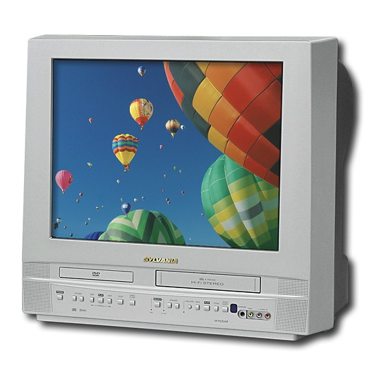
When servicing the deck I Specifications mechanism, refer to MK14 Deck I Preparation for Servicing Mechanism Section. I Adjustment Procedures I Schematic Diagrams Deck Mechanism Part No.: I CBA’s I Exploded Views N2466FT I Parts List 20″ COLOR TV/DVD/VCR 6720FDF... -
Page 2: Important Safety Notice
IMPORTANT SAFETY NOTICE Proper service and repair is important to the safe, reliable operation of all Funai Equipment. The service procedures recommended by Funai and described in this service manual are effective methods of performing service operations. Some of these service special tools should be used when and as recommended. -
Page 3: Table Of Contents
MAIN SECTION 20″ COLOR TV/DVD/VCR 6720FDF Main Section I Specifications I Preparation for Servicing I Adjustment Procedures I Schematic Diagrams I CBA’s I Exploded Views I Parts List TABLE OF CONTENTS Specifications ................1-1-1 Laser Beam Safety Precautions . -
Page 4: Specifications
SPECIFICATIONS *ˆ Mode---------SP mode unless otherwise specified * Test input terminal <Except Tuner>--------Video input (1 Vp-p) Audio input (-10 dB) <Tuner>------------------Ant. input (80 dBµV) Video: 87.5% Audio: 25 kHz dev. (1 kHz Sin) < DEFLECTION > Description Condition Unit Nominal Limit 1. - Page 5 < VCR > Description Condition Unit Nominal Limit 1. Horizontal Resolution (R/P, SP) Line µs 2. Jitter (Low) (R/P, SP) AM(SP) (R/P, SP) 3. S/N Chroma PM(SP) (R/P, SP) 4. Wow & Flutter (JIS, UNWTD) (R/P, SP) 0.25 < TUNER > Description Condition Unit...
-
Page 6: Laser Beam Safety Precautions
LASER BEAM SAFETY PRECAUTIONS This DVD player uses a pickup that emits a laser beam. Do not look directly at the laser beam coming from the pickup or allow it to strike against your skin. The laser beam is emitted from the location shown in the figure. When checking the laser diode, be sure to keep your eyes at least 30 cm away from the pickup lens when the diode is turned on. -
Page 7: Important Safety Precautions
IMPORTANT SAFETY PRECAUTIONS Prior to shipment from the factory, our products are strictly inspected for recognized product safety and electrical codes of the countries in which they are to be sold. However, in order to maintain such compliance, it is equally important to implement the following precautions when a set is being serviced. - Page 8 Also, because the picture tube shields and an isolation transformer only if the AC power mounting hardware perform an X-radiation plug is inserted so that the chassis is protection function, they must be correctly in connected to the ground side of the AC power place.
- Page 9 of the countries in which they are to be sold. 2) Strip about 15 mm of the insulation from the However, in order to maintain such compliance, it ends of the wires. If the wires are stranded, is equally important to implement the following twist the strands to avoid frayed conductors.
- Page 10 Safety Check after Servicing Examine the area surrounding the repaired location for damage or deterioration. Observe that screws, parts and wires have been returned to original positions. Afterwards, perform the following tests and confirm the specified values in order to verify compliance with safety standards. 1.
-
Page 11: Standard Notes For Servicing
STANDARD NOTES FOR SERVICING Circuit Board Indications Pb (Lead) Free Solder 1. The output pin of the 3 pin Regulator ICs is Pb free mark will be found on PCBs which use Pb indicated as shown. free solder. (Refer to figure.) For PCBs with Pb free mark, be sure to use Pb free solder. - Page 12 around the flat pack-IC to protect other parts from With Soldering Iron: damage. (Fig. S-1-2) 1. Using desoldering braid, remove the solder from 3. The flat pack-IC on the CBA is affixed with glue, so all pins of the flat pack-IC. When you use solder be careful not to break or damage the foil of each flux which is applied to all pins of the flat pack-IC, pin or the solder lands under the IC when...
- Page 13 2. Installation With Iron Wire: 1. Using desoldering braid, remove the solder from 1. Using desoldering braid, remove the solder from all pins of the flat pack-IC. When you use solder the foil of each pin of the flat pack-IC on the CBA flux which is applied to all pins of the flat pack-IC, so you can install a replacement flat pack-IC more you can remove it easily.
- Page 14 Instructions for Handling Semi- conductors Electrostatic breakdown of the semi-conductors may occur due to a potential difference caused by electrostatic charge during unpacking or repair work. 1. Ground for Human Body Be sure to wear a grounding band (1 MΩ) that is properly grounded to remove any static electricity that may be charged on the body.
-
Page 15: Preparation For Servicing
PREPARATION FOR SERVICING How to Enter the Service Mode Adjustment Mode Caution 1: Head switching position adjustment: See adjustment instructions page 1-7-8. 1. Optical sensors system are used for Tape Start and End Sensor on this equipment. Read this No need to use. page carefully and prepare as described on this Purity check mode: Shows Red, Green, page before starting to service;... -
Page 16: Cabinet Disassembly Instructions
CABINET DISASSEMBLY INSTRUCTIONS 1. Disassembly Flowchart Removal Step/ This flowchart indicates the disassembly steps for the Remove/*Unhook/ Loc. Part Fig. Unlock/Release/ cabinet parts, and the CBA in order to gain access to Note Unplug/Unclamp/ item(s) to be serviced. When reassembling, follow the Desolder steps in reverse order. - Page 17 Reference Notes in the Table 1) Disconnect Connector (CN301) on the DVD Main CBA Unit. CAUTION! 2) Short the three short lands of FPC cable with When removing the CRT, be sure to discharge the solder before removing the FFC cable (CN201) Anode Lead of the CRT with the CRT Ground Wire from it.
- Page 18 (S-5) Wire Holder C [2] Tray Chassis Unit (S-6) Loader Cover (S-5) [4] DVD (S-9) Mechanism (S-9) (S-7) Loader PCB Holder Top Shield [5] DVD Main CBA Unit (S-10) (S-10) (S-7) [8] Deck Assembly (S-7) (S-10) (S-7) (S-8) (S-13) (S-13) [6] Sub CBA [7] Function CBA (S-13)
- Page 19 Anode Cap (S-4) CRT CBA (S-4) (S-4) [3] CRT (S-4) Fig. D3 DVD Mechanism Short the three short lands by soldering. (Either of two places.) View for A Connector Fig. D4 1-6-4 T1100DC...
- Page 20 DVD MAIN CBA UNIT CN201 CN301 CN2A CN1A TO SPEAKER ANODE CN2801 CN2571 CL2501A SUB CBA CN2503 CN2502 CN2401 FOCUS MAIN CBA CL403 CN1301 CN1602 CN1803 CL2504A CN1302 CL2501B CL1401 SCREEN CN2501 CRT CBA CL1402 CN1601 AC CORD CL1201 CN1802 TUNER TO SPEAKER ACE HEAD...
-
Page 21: Electrical Adjustment Instructions
ELECTRICAL ADJUSTMENT INSTRUCTIONS General Note: “CBA” is abbreviation for How to Set up the Service mode: “Circuit Board Assembly.” Service mode: Note: Electrical adjustments are required after 1. Use the service remote control unit. replacing circuit components and certain mechanical parts. It is important to perform 2. - Page 22 2. Setting for CONTRAST, COLOR, 3. C-Trap Adjustment TINT, V-TINT and SHARP Data Purpose: To get minimum leakage of the color signal Values carrier. Symptom of Misadjustment: If C-Trap Adjustment is General incorrect, stripes will appear on the screen. 1. Enter the Service mode. (See page 1-7-1.) Test Point Adj.
- Page 23 4. Setting for Y DL Time TV, Y DL Time EXT, Y SW LPF, Black C-TRAP Adjustment (Factory mode) Stretch Off, Black Stretch CONT and C. Angle Data Values button button C-TRP 0 C-TRP 1 1. Enter the Service mode. (See page 1-7-1.) 2.
- Page 24 5. Setting for CD-VOL, DVD-BRT, DVD-CNT and DVD-SHARP Data CD-VOL Adjustment (Factory mode) Values [VOL 1. Enter the Service mode. (See page 1-7-1.) button button CD VOL CD VOL 2. CD-VOL Adjustment: Press [VOL o] button on the service remote control unit once to show “CD button VOL”...
- Page 25 6. H f Adjustment 7. Cut-off Adjustment Purpose: To get correct horizontal position and size of Purpose: To adjust the beam current of R, G, B, and screen image. screen voltage. Symptom of Misadjustment: Horizontal position and Symptom of Misadjustment: White color may be size of screen image may not be properly displayed.
-
Page 26: White Balance Adjustment
8. White Balance Adjustment 9. Sub-Brightness Adjustment Purpose: To mix red, green and blue beams correctly Purpose: To get proper brightness. for pure white. Symptom of Misadjustment: If Sub-Brightness is Symptom of Misadjustment: White becomes bluish incorrect, proper brightness cannot be obtained by or reddish. -
Page 27: Focus Adjustment
10. Focus Adjustment 12. V. Shift Adjustment Purpose: Set the optimum Focus. Purpose: To obtain correct vertical position of screen image. Symptom of Misadjustment: If Focus Adjustment is incorrect, blurred images are shown on the display. Symptom of Misadjustment: If V. position is incorrect, vertical position of image on the screen may Test Point Adj. -
Page 28: Purity Adjustment
14. Head Switching Position The following 2 adjustments normally are not attempted in the field. They should be done only Adjustment when replacing the CRT then adjust as a preparation. Purpose: Determine the Head Switching Position during Playback. 15. Purity Adjustment Symptom of Misadjustment: May cause Head Purpose: To obtain pure color. -
Page 29: Convergence Adjustment
16. Convergence Adjustment 4. Fix the C.P. Magnets by tightening the Ring Lock. 5. Remove the DY Wedges and slightly tilt the Purpose: To obtain proper convergence of red, green Deflection Yoke horizontally and vertically to and blue beams. obtain the best overall convergence. Symptom of Misadjustment: If Convergence 6. -
Page 30: How To Initialize The Tv/Dvd/Vcr
HOW TO INITIALIZE THE TV/DVD/VCR To put the program back at the factory-default, initialize the TV/DVD/VCR as the following procedure. < DVD Section > < TV/VCR Section > 1. Turn the power on and press [SELECT] button on 1. Use the service remote control unit. the remote control unit to put the TV/DVD/VCR 2. -
Page 31: Firmware Renewal Mode
FIRMWARE RENEWAL MODE 1. Turn the power on and press [SELECT] button on " ******* " differ depending on the models. the remote control unit to put the TV/DVD/VCR into DVD mode. Then remove the disc on the tray. F/W Version Up Mode Model No : ******* (It is possible to move to F/W version up mode VERSION : *.**... -
Page 32: Block Diagrams
BLOCK DIAGRAMS < TV/VCR Section > System Control / Servo Block Diagram 1-10-1 T1100BLS... - Page 33 Video Block Diagram 1-10-2 T1100BLV...
- Page 34 Audio Block Diagram 1-10-3 T1100BLA...
- Page 35 Hi-Fi Audio Block Diagram 1-10-4 T1100BLH...
- Page 36 TV Process Block Diagram 1-10-5 T1100BLT...
- Page 37 CRT/H.V. Block Diagram 1-10-6 T1100BLCRT...
- Page 38 Power Supply Block Diagram 1-10-7 T1100BLP...
- Page 39 BLOCK DIAGRAMS < DVD Section > DVD System Control / Servo Block Diagram 1-10-8 T1100BLSD...
- Page 40 Digital Signal Process Block Diagram 1-10-9 T1100BLD...
- Page 41 DVD Audio Block Diagram 1-10-10 T1100BLAD...
-
Page 42: Schematic Diagrams / Cba's And Test Points
SCHEMATIC DIAGRAMS / CBA’S AND TEST POINTS Standard Notes WARNING Many electrical and mechanical parts in this chassis have special characteristics. These characteristics often pass unnoticed and the protection afforded by them cannot necessarily be obtained by using replacement components rated for higher voltage, wattage, etc. - Page 43 LIST OF CAUTION, NOTES, AND SYMBOLS USED IN THE SCHEMATIC DIAGRAMS ON THE FOLLOWING PAGES: 1. CAUTION: FOR CONTINUED PROTECTION AGAINST RISK OF FIRE, REPLACE ONLY WITH SAME TYPE_A,_V FUSE. ATTENTION: UTILISER UN FUSIBLE DE RECHANGE DE MÊME TYPE DE_A,_V. 2.
- Page 44 Main 1/6 Schematic Diagram < TV/VCR Section > MAIN 1/6 Ref No. Position IC1201 IC1202 TRANSISTORS Q1205 Q1206 CONNECTOR CL1201 TEST POINT TP1202 T1100SCM1 1-11-3...
- Page 45 Main 2/6 Schematic Diagram < TV/VCR Section > MAIN 2/6 Ref No. Position IC1401 TRANSISTORS Q1401 Q1402 Q1403 Q1404 Q1871 Q1872 Q1873 Q1874 Q1875 CONNECTORS CL403 CL1401 CL1402 TEST POINTS JM1403 TP1401 TP1402 T1100SCM2 1-11-4...
- Page 46 Main 3/6 Schematic Diagram < TV/VCR Section > MAIN 3/6 Ref No. Position IC1001 IC1301 TRANSISTOR Q1350 CONNECTOR CN1302 TEST POINTS TP1301 TP1302 TP1303 T1100SCM3 1-11-5...
- Page 47 Main 4/6 Schematic Diagram < TV/VCR Section > MAIN 4/6 Ref No. Position IC1701 TRANSISTOR Q1701 TEST POINTS TP1701 TP1702 TP1703 T1100SCM4 1-11-6...
- Page 48 Main 5/6 Schematic Diagram < TV/VCR Section > MAIN 5/6 Ref No. Position IC1803 CONNECTORS CN1301 BB-3 CN1802 CN1803 BB-4 TEST POINTS TP1001 TP1002 TP1671 BB-3 TP1672 BB-3 TP1673 BB-3 T1100SCM5 1-11-7...
- Page 49 Main 6/6 Schematic Diagram < TV/VCR Section > VOLTAGE CHART (Power off mode) Ref. No. CAUTION ! IC1601 12.0 10.9 Ref. No. Fixed voltage (or Auto voltage selectable) power supply circuit is used in this unit. CAUTION ! : For continued protection against risk of fire, IC1682 If Main Fuse (F1601) is blown , check to see that all components in the power supply replace only with same type 4 A, 125V fuse.
- Page 50 Sub 1/2 Schematic Diagram < TV/VCR Section > SUB 1/2 Ref No. Position IC2551 TRANSISTORS Q2571 Q2591 Q2592 CONNECTORS CL2501A CN2571 TEST POINTS TP2501 TP2502 TP2503 TP2504 TP2505 1-11-9 T1100SCSUB1...
- Page 51 Sub 2/2 Schematic Diagram < TV/VCR Section > SUB 2/2 Ref No. Position IC2602 IC3603 IC3604 TRANSISTORS Q2610 Q2611 Q2612 Q2615 Q2616 Q2617 CONNECTORS CN2502 CN2503 T1100SCSUB2 1-11-10...
- Page 52 CRT Schematic Diagram < TV/VCR Section > Ref No. Position TRANSISTORS Q2501 Q2502 Q2503 CONNECTORS CL2501B CL2504A CN2501 T1100SCCRT Function Schematic Diagram < TV/VCR Section > T1100SCF 1-11-11...
- Page 53 DVD Main 1/3 Schematic Diagram < DVD Section > 1 NOTE: Either IC461 or IC462 is used for DVD MAIN CBA UNIT. DVD MAIN 1/3 Ref No. Position IC201 IC202 IC301 IC461 IC462 TRANSISTORS Q001 Q002 Q003 Q251 Q252 Q253 Q254 CONNECTORS CN1A...
- Page 54 DVD Main 2/3 Schematic Diagram < DVD Section > DVD MAIN 2/3 Ref No. Position IC101 T1100SCD2 1-11-13...
- Page 55 IC101 Voltage Chart ~ : Voltage is not consistent ----- : Not used Unit : Volts PIN.NO PLAY STOP PIN.NO PLAY STOP PIN.NO PLAY STOP PIN.NO PLAY STOP PIN.NO PLAY STOP PIN.NO PLAY STOP PIN.NO PLAY STOP PIN.NO PLAY STOP ----- ----- -----...
- Page 56 DVD Main 3/3 Schematic Diagram < DVD Section > DVD MAIN 3/3 Ref No. Position IC103 IC501 IC502 IC601 TRANSISTORS Q004 Q005 CONNECTOR CN2A T1100SCD3 1-11-15...
- Page 57 Main CBA Top View < TV/VCR Section > Sensor CBA Top View CAUTION ! : For continued protection against risk of fire, NOTE: replace only with same type 4 A, 125V fuse. The voltage for parts in hot circuit is measured using Because a hot chassis ground is present in the power 4A 125V ATTENTION : Utiliser un fusible de rechange de même type de 4A, 125V.
- Page 58 Main CBA Bottom View < TV/VCR Section > CAUTION ! : For continued protection against risk of fire, NOTE: replace only with same type 4 A, 125V fuse. Because a hot chassis ground is present in the power The voltage for parts in hot circuit is measured using 4A 125V ATTENTION : Utiliser un fusible de rechange de même type de 4A, 125V.
- Page 59 Sub CBA Top View < TV/VCR Section > SUB CBA Ref No. Position IC2551 IC2602 IC3603 IC3604 TRANSISTORS Q2571 Q2591 Q2592 Q2610 Q2611 TP2501 Q2612 Q2615 Q2616 Q2617 CONNECTORS CL2501A CN2502 CN2503 CN2571 TEST POINTS TP2501 TP2502 TP2503 TP2504 TP2505 R2583 (H f Adjustment)
- Page 60 Sub CBA Bottom View < TV/VCR Section > TP2503 H-DRIVE WF20 J2537 SPDIF WF11 PIN 5 CN2571 WF10 Q2571 Collector BT1100F01022-A 1-11-19...
- Page 61 CRT CBA Top View < TV/VCR Section > CRT CBA Bottom View < TV/VCR Section > CRT CBA Ref No. Position TRANSISTORS Q2501 Q2502 Q2503 CONNECTORS CL2501B CL2504A CN2501 WF12 WF14 WF13 Q2503 Q2502 Q2501 Collector Collector Collector BT1100F01022-B 1-11-20...
- Page 62 Function CBA Top View < TV/VCR Section > Function CBA Bottom View < TV/VCR Section > BT1100F01022-C Junction CBA Top View Junction CBA Bottom View BT1100F01022 1-11-21...
-
Page 63: Waveforms
WAVEFORMS X6TWF 1-12-1... -
Page 64: Wiring Diagram < Vcr Section
WIRING DIAGRAM < TV/VCR Section > T1100WIT 1-13-1... -
Page 65: Wiring Diagram < Dvd Section
WIRING DIAGRAM < DVD Section > T1100WID 1-13-2... -
Page 66: System Control Timing Charts
SYSTEM CONTROL TIMING CHARTS < VCR Section > Mode SW: LD-SW LD-SW Position detection A/D Input voltage Limit Symbol (Calculated voltage) 3.76 V ~ 4.50 V (4.12 V) 4.51 V ~ 5.00 V (5.00 V) 0.00 V ~ 0.25 V (0.00 V) 1.06 V ~ 1.50 V (1.21 V) 0.66 V ~ 1.05 V (0.91 V) 1.99 V ~ 2.60 V (2.17 V) - Page 67 Chart 1 1) SP MODE 18 RF-SW The first rise of RF-SW after a rise in F-AD signal. F-AD ( Internal Signal ) "H" "H" "Z" C-DRIVE Stop Detection Acceleration Detection Slow Tracking Value PB CTL Reversal Limit Value 66 C-F/R ROLL COMPENSATION (DRUM SERVO)
- Page 68 Chart 2 2) LP/EP MODE 18 RF-SW The first rise of RF-SW after a rise in F-AD signal. F-AD ( Internal Signal ) "H" "H" "Z" C-DRIVE Stop Detection Acceleration Detection Slow Tracking Value PB CTL Reversal Limit Value 66 C-F/R ROLL COMPENSATION (DRUM SERVO)
- Page 69 Chart 3 EJECT ST-S/ END-S "OFF" CASS.LOAD LD-FWD 0.2S LD-REV SFT-SW STOP(B) POWER LD-FWD 0.4S 0.2S LD-REV 0.2S LD-FWD 0.5S LD-REV STOP(A) PLAY LD-FWD PLAY LD-FWD RS1(RS2) LD-REV 0.2S LD-FWD FS1(FS2) PLAY PLAY PAUSE (SLOW) LD-FWD STILL(SLOW) PLAY LD-REV 0.2S LD-FWD PLAY STOP...
- Page 70 Chart 4 STOP(A) STOP LD-REV 0.2S LD-FWD 0.2S STOP /EJECT 1.0S LD-FWD 0.5S LD-REV STOP(A) LD-REV 0.2S LD-FWD 0.2S STOP /EJECT LD-REV 1.0S LD-FWD 0.5S LD-REV STOP(A) LD-FWD PAUSE LD-FWD 2.5S Short REV LD-REV 0.2S LD-FWD REC PAUSE REC or PAUSE STOP /EJECT...
- Page 71 < DVD Section > Tray Close ~ Play / Play ~ Tray Open Tray Disc Disc Tray Play Close Rotation Stop Open 3.3V Tray IN (TL221) Sled Drive 1.65V (TP303) 1.65V Disc Drive (TP301) 1.65V Focus Drive (TP304) 1.65V Tracking Drive (TP302) 1-14-6 X6T4HTI...
-
Page 72: Ic Pin Function Descriptions
IC PIN FUNCTION DESCRIPTIONS IC1201 (TV/VCR Micro Controller IC) Signal Function Name “H” ≥ 4.5 V, “L” ≤ 1.0 V Not Used Signal REC- Record Protection Tab Function Name SAFETY Detection IN LD-SW Loading Switch Input System Reset Signal (Reset IN RESET = “L”) OUT DVD-LED... - Page 73 Signal Signal Function Function Name Name D-REC-L/ P-SAFETY Power Supply Failure 67 OUT Recording/Playback Output PLAY-H Detection 1 68 OUT YCA-SDA YCA IC Control Data 69 OUT YCA-CS YCA IC Control Chip Select 70 OUT YCA-SCL YCA IC Control Clock E2PROM/CHROMA IC Tuner 71 OUT SCL Communication Clock...
-
Page 74: Lead Identifications
LEAD IDENTIFICATIONS 2SD400(F) PQ070XF01SZ 2SK3563 MID-32A22F AN17812A 1: Vin 2: Vo 3: GND 1 2 3 4 E C B 4: Vc S D G 2SC2120-O-TPE2 2SA1175(F) LA78040A 2SA950(O) 2SC1627Y-TPE2 2SC2482 TPE6 2SC2785(F) 2SC3331(T) KRA103M KRC103M KTC3199(GR) E C B E C B M3776AMCH-BA2GP KIA431-AT... -
Page 75: Exploded Views
EXPLODED VIEWS Cabinet SHINWHA TAPE SGT-730 (BLACK) Details for L551 V501-2 and surrounding parts SHINWHA TAPE SGT-730 V501-1 (WHITE) L551 V501-3 CRT CBA TB18 Scotch TB23-2 Tape #880 L3-1 CLN551 CLN551 CLN551 TB14 L3-2 DVD Main TL1-5 CBA Unit TL1-1 Scotch TL1-1 Tape #880... - Page 76 Packing Packing Tape Tape 1-17-2 T1100PEX...
-
Page 77: Mechanical Parts List
0EM402178 A1-1 FRONT CABINET T1050UA 1EM020067 HOLD PAD T1100UA 1EM420618 A1-2 CONTROL PLATE T1100UA 1EM220076 ACCESSORIES A1-3 BADGE L BRAND TD951UB~SYLVANIA~ 0EM408107 BAG POLYETHYLENE 235X365XT0.03 0EM408420 A1-4 CASSETTE DOOR TD851UB 0EM408098 OWNER'S MANUAL T1100UA 1EMN20212 A1-5 SPRING DOOR(Z10) T5200UA 0EM406687... -
Page 78: Electrical Parts List
ELECTRICAL PARTS LIST PRODUCT SAFETY NOTE: Products marked with a Ref. No. Description Part No. # have special characteristics important to safety. C1114 CHIP CERAMIC CAP .(1608) B K 1000pF/50V CHD1JK30B102 Before replacing any of these components, read C1115 PCB JUMPER D0.6-P5.0 JW5.0T carefully the product safety notice in this service C1116... - Page 79 Ref. No. Description Part No. Ref. No. Description Part No. C1336 STACKED FILM CAP . 0.47µF/50V J CMA1JJS00474 C1616 ELECTROLYTIC CAP . 100µF/160V M CE2CMZPDL101 C1337 CHIP CERAMIC CAP .(1608) B K 0.01µF/50V CHD1JK30B103 C1617# ELECTROLYTIC CAP . 470µF/35V M CE1GMASDL471 C1338 CHIP CERAMIC CAP .
- Page 80 Ref. No. Description Part No. Ref. No. Description Part No. C1787 ELECTROLYTIC CAP . 22µF/16V M H7 CE1CMAVSL220 D1606# DIODE 1N5406 NDLZ001N5406 C1788 ELECTROLYTIC CAP . 4.7µF/50V M H7 CE1JMAVSL4R7 D1607# ZENER DIODE MTZJT-7724C QDTC00MTZJ24 C1789 ELECTROLYTIC CAP . 22µF/16V M H7 CE1CMAVSL220 D1609# SWITCHING DIODE 1SS133(T-77)
- Page 81 Ref. No. Description Part No. Ref. No. Description Part No. CHIP RES. 1/16W G 3.6k Ω L1405 INDUCTOR 47µH-J-26T LLAXJATTU470 R1205 RRXAGR5Z0362 CHIP RES. 1/16W G 10k Ω L1601# LINE FILTER 2.7MH ELF15N013A LLBG00ZMS037 R1206 RRXAGR5Z0103 CHIP RES.(1608) 1/10W J 100k Ω L1751 PCB JUMPER D0.6-P5.0 JW5.0T...
- Page 82 Ref. No. Description Part No. Ref. No. Description Part No. CHIP RES.(1608) 1/10W J 1k Ω CHIP RES.(1608) 1/10W J 1.2k Ω R1277 RRXAJR5Z0102 R1429 RRXAJR5Z0122 CHIP RES.(1608) 1/10W J 1k Ω CHIP RES.(1608) 1/10W J 1k Ω R1280 RRXAJR5Z0102 R1430 RRXAJR5Z0102 CHIP RES.(1608) 1/10W J 100k Ω...
- Page 83 Ref. No. Description Part No. Ref. No. Description Part No. CARBON RES. 1/2W J 18 Ω R1694 RCX2JZQZ0180 BC1602 PCB JUMPER D0.6-P5.0 JW5.0T R1695 PCB JUMPER D0.6-P5.0 JW5.0T BC1604 PCB JUMPER D0.6-P5.0 JW5.0T CARBON RES. 1/4W J 75 Ω R1701 RCX4JATZ0750 BC1605 BEAD INDUCTORS FBA04HA600VB-00...
- Page 84 MPS CBA Ref. No. Description Part No. D2597# SWITCHING DIODE 1SS133(T-77) QDTZ001SS133 Ref. No. Description Part No. D2598# DIODE FR104-B NDLZ000FR104 MPS CBA 1ESA10436 D2601 SWITCHING DIODE 1SS133(T-77) QDTZ001SS133 Consists of the following: D2602 SWITCHING DIODE 1SS133(T-77) QDTZ001SS133 SUB CBA (MPS-A) ---------- CRT CBA (MPS-B) ----------...
- Page 85 Ref. No. Description Part No. Ref. No. Description Part No. CARBON RES. 1/4W J 180 Ω R2576 RCX4JATZ0181 X6 H-HEAT SINK PJZ T1100UA 1EM420564 CARBON RES. 1/4W J 180 Ω R2577 RCX4JATZ0181 SCREW, B-TIGHT D3X8 BIND HEAD+ GBMB3080 CARBON RES. 1/4W J 56 Ω R2580# RCX4JATZ0560 JK2601...
- Page 86 FUNCTION CBA Ref. No. Description Part No. FUNCTION CBA (MPS-C) ---------- Consists of the following: CONNECTORS CN2401 BOARD CONNECTOR 07P(PB FREE) JCTWA07TG004 127301107K2 CN2801 STRAIGHT CONNECTOR BASE 00 8283 0212 J383C02UG002 00 000 RESISTORS CARBON RES. 1/4W G 1.5k Ω R2401 RCX4GATZ0152 CARBON RES.
- Page 87 6720FDF T1100UA 2005-03-26...