Table of Contents
Advertisement
Quick Links
CDX-GT450U/GT454US
SERVICE MANUAL
Ver. 1.0 2010.10
• The tuner and CD sections have no adjustments.
AUDIO POWER SPECIFICATIONS
(US model)
CEA2006 Standard
Power Output: 17 Watts RMS × 4 at
4 Ohms < 1 % THD + N
SN Ratio: 80 dBA
(reference: 1 Watt into 4 Ohms)
Tuner section
FM
Tuning range:
US, CND model: 87.5 – 107.9 MHz
RU model: 87.5 – 108.0 MHz
Antenna (aerial) terminal:
External antenna (aerial) connector
Intermediate frequency: 150 kHz
Usable sensitivity: 10 dBf
Selectivity: 75 dB at 400 kHz
Signal-to-noise ratio: 70 dB (mono)
Separation: 40 dB at 1 kHz
Frequency response: 20 – 15,000 Hz
9-889-981-01
Sony Corporation
2010J04-1
©
2010.10
Published by Sony Techno Create Corporation
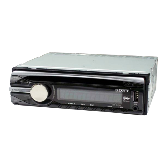
Photo: CDX-GT450U
SPECIFICATIONS
AM (US, CND model)
Tuning range: 530 – 1,710 kHz
Antenna (aerial) terminal:
External antenna (aerial) connector
Intermediate frequency: 25 kHz
Sensitivity: 26 μV
MW/LW (RU model)
Tuning range:
MW: 531 – 1,602 kHz
LW: 153 – 279 kHz
Antenna (aerial) terminal:
External antenna (aerial) connector
Intermediate frequency: 25 kHz
Sensitivity: MW: 26 μV, LW: 45 μV
FM/AM COMPACT DISC PLAYER
FM/MW/LW COMPACT DISC PLAYER
Canadian Model
Russian Model
Model Name Using Similar Mechanism
CD Drive Mechanism Type
Optical Pick-up Name
CD Player section
Signal-to-noise ratio: 120 dB
Frequency response: 10 – 20,000 Hz
Wow and fl utter: Below measurable limit
USB Player section
Interface: USB (Full-speed)
Maximum current: 500 mA
Power amplifi er section
Outputs: Speaker outputs
Speaker impedance: 4 – 8 ohms
Maximum power output:
52 W × 4 (at 4 ohms)
– Continued on next page –
US Model
CDX-GT450U
CDX-GT454US
NEW
MG-101N-188
DAX-25A
US, Canadian model
Russian model
Advertisement
Table of Contents

Related Manuals for Sony CDX-GT454US


Summary of Contents for Sony CDX-GT454US
- Page 1 Intermediate frequency: 25 kHz Sensitivity: MW: 26 μV, LW: 45 μV – Continued on next page – US, Canadian model FM/AM COMPACT DISC PLAYER Russian model FM/MW/LW COMPACT DISC PLAYER 9-889-981-01 Sony Corporation 2010J04-1 © 2010.10 Published by Sony Techno Create Corporation...
- Page 2 LES DIAGRAMMES SCHÉMATIQUES ET LA LISTE DES PIÈCES SONT CRITIQUES POUR LA SÉCURITÉ DE FONC- TIONNEMENT. NE REMPLACER CES COMPOSANTS QUE PAR DES PIÈCES SONY DONT LES NUMÉROS SONT DON- NÉS DANS CE MANUEL OU DANS LES SUPPLÉMENTS PUBLIÉS PAR SONY.
-
Page 3: Table Of Contents
CDX-GT450U/GT454US Russian model: TABLE OF CONTENTS SERVICE NOTE ............GENERAL Connections ..............This label is located on the bottom of the chassis. DISASSEMBLY 3-1. Sub Panel Assy ............... 3-2. CD Mechanism Block ............. 3-3. Main Board ..............UNLEADED SOLDER 3-4. Servo Board ..............Boards requiring use of unleaded solder are printed with the lead- 3-5. -
Page 4: Service Note
CDX-GT450U/GT454US SECTION 1 SERVICE NOTE EXTENSION CABLE AND SERVICE POSITION When repairing or servicing this set, connect the jig (extension cable) as shown below. • Connect the MAIN board (CN701) and the SERVO board (CN401) with the extension cable (Part No. J-2502-076-1). MAIN BOARD CN701 J-2502-076-1... -
Page 5: General
CDX-GT450U/GT454US SECTION 2 GENERAL This section is extracted from instruction manual. • CONNECTIONS • US, Canadian model RCA pin cord (not supplied). Cordon à broche RCA (non fourni). AUDIO OUT can be switched SUB or REAR. For AUDIO OUT peut être commuté sur SUB ou details, see the supplied Operating Instructions. - Page 6 CDX-GT450U/GT454US • CONNECTIONS • Russian model R AR R AR REMOTE REAR / SUB AUDIO OUT (10 A AMP REM 0 3 A “Cx ” “ ” T (T LURE ( LURE...
-
Page 7: Disassembly
CDX-GT450U/GT454US SECTION 3 DISASSEMBLY • This set can be disassembled in the order shown below. 3-1. SUB PANEL ASSY (Page 8) 3-2. CD MECHANISM BLOCK (Page 8) 3-4. SERVO BOARD 3-3. MAIN BOARD (Page 9) (Page 9) 3-5. CHASSIS (T) SUB ASSY (Page 10) 3-6. -
Page 8: Sub Panel Assy
CDX-GT450U/GT454US Note: Follow the disassembly procedure in the numerical order given. 3-1. SUB PANEL ASSY 3 two claws 2 two claws 1 two screws (+PTT 2.6 4 sub panel assy 3-2. CD MECHANISM BLOCK 7 bracket (CD) 8 CD mechanism block 6 two screws (+PTT 2.6 5 wire (flat type) (13 core) -
Page 9: Main Board
CDX-GT450U/GT454US 3-3. MAIN BOARD 2 two screws (+PTT 2.6 4 two screws (+P 2.6 5 two screws (+PTT 2.6 1 three ground point screws 6 screw (+PTT 2.6 (+P 2.6 7 screw (+PTT 2.6 8 heat sink 9 MAIN board insulating sheet 3-4. -
Page 10: Chassis (T) Sub Assy
CDX-GT450U/GT454US 3-5. CHASSIS (T) SUB ASSY 2 two screws 1 two screws (M 1.7 2.5) (M 1.7 2.5) 4 chassis (T) sub assy 3 claw 3-6. ROLLER ARM ASSY 6 roller arm assy 4 gear (RA1) 1 spring (RAL) 3 washer 2 spring (RAR) -
Page 11: Chassis (Op) Assy
CDX-GT450U/GT454US 3-7. CHASSIS (OP) ASSY 6 chassis (OP) assy 1 tension spring (KF) 7 two coil springs (damper) (natural) 8 coil spring (damper) (green) 4 slider (R) 3 lever (D) 2 gear (LE1) 3-8. CHUCKING ARM SUB ASSY 3 chucking arm sub assy 1 spring Note: Have this portion receive the chassis. -
Page 12: Sled Motor Assy
CDX-GT450U/GT454US 3-9. SLED MOTOR ASSY 2 three serration screws (M 2 3 sled motor assy 1 spring turn table spring stand Note: Never remove these parts since they were adjusted. bearing (F) stand Note: Place the stand with care not to touch the turn table. bearing (R) Note for Assembly three serration screws... -
Page 13: 3-10. Optical Pick-Up Section
CDX-GT450U/GT454US 3-10. OPTICAL PICK-UP SECTION 2 optical pick-up section Note: Be careful not to touch the lens and hologram terminal when removing the optical pick-up section. 3-11. OPTICAL PICK-UP 1 tapping screw (P 1.4) 2 leaf spring (OPS) 3 rack 5 optical pick-up 4 lead screw assy... -
Page 14: Diagrams
CDX-GT450U/GT454US SECTION 4 DIAGRAMS THIS NOTE IS COMMON FOR PRINTED WIRING • Waveforms BOARDS AND SCHEMATIC DIAGRAMS. – MAIN Board – (In addition to this, the necessary note is printed in each block.) IC501 qa (XOUT) For Printed Wiring Boards. Note: •... -
Page 15: Block Diagram -Main Section
CDX-GT450U/GT454US 4-1. BLOCK DIAGRAM – MAIN Section – GT454US ELECTRONIC VOLUME J401 IC401 AUDIO REAR/SUB R-CH GT450U AU_OUT_SL REAR/SUB J402 R-CH AU_OUT_SR R-CH (REAR/SUB) J901 R-CH AUDIO 5 AUX_LCH R-CH 7 AUX_RCH I2C BUS CONTROLLED FRONT POWER AMP/MULTIPLE R-CH MUTE 6 AUX_GND VOLTAGE REGULATOR Q406... -
Page 16: Block Diagram -Display Section
CDX-GT450U/GT454US 4-2. BLOCK DIAGRAM – DISPLAY Section – SYSTEM CONTROL LCD DRIVER,LED CONTROL IC501 (2/2) IC901 KEYIN1 SEG48 KEY MATRIX LCD901 LSW905–912, LCD_SO SEG1 DATA LIQUID PANEL+B S901–907 KEYIN0 CRYSTAL LCD_CLK CLK LCD DISPLAY LED903,905,907,909, LCD_CE 92 KEYACK1 PANEL 910,912,914,916,919, COM4 LED901 921,925,928,929,932,... -
Page 17: Printed Wiring Board -Main Section
CDX-GT450U/GT454US 4-3. PRINTED WIRING BOARD – MAIN Section – • : Uses unleaded solder. J401 (GT454US) AUDIO OUT J402 (GT450U) AUDIO OUT REAR/SUB FRONT GT450U J801 (REMOTE IN) JW300 JC277 CN301 C320 R441 C412 C330 C319 C323 JW293 C423 C304 FB826 R403 C421... -
Page 18: Schematic Diagram -Main Section (1/3)
CDX-GT450U/GT454US 4-4. SCHEMATIC DIAGRAM – MAIN Section (1/3) – • See page 23 for IC Block Diagrams. GT454US GT450U MAIN BOARD (1/3) RL– FRONT IC301 IC B/D L-CH – FL– IC301 REAR TDF8556AJ/N3 L-CH – I2C BUS CONTROLLED FR– POWER AMP/MULTIPLE REAR VOLTAGE REGULATOR R-CH... -
Page 19: Schematic Diagram -Main Section (2/3)
CDX-GT450U/GT454US 4-5. SCHEMATIC DIAGRAM – MAIN Section (2/3) – • See page 14 for Waveforms. • See page 24 for IC Block Diagrams. • See page 26 for IC Pin Function Description of IC501. (Page 18) MAIN BOARD (1/3) MAIN BOARD (2/3) CD MECHANISM UNIT (MG-101N) -
Page 20: Schematic Diagram -Main Section (3/3)
CDX-GT450U/GT454US 4-6. SCHEMATIC DIAGRAM – MAIN Section (3/3) – • See page 14 for Waveforms. • See page 24 for IC Block Diagrams. MAIN BOARD (3/3) GT450U J402 C426 100p FRONT C421 100p R441 R406 C423 100p AUDIO OUT Q401 Q402 Q403 Q404... -
Page 21: Printed Wiring Board -Key Section
CDX-GT450U/GT454US 4-7. PRINTED WIRING BOARD – KEY Section – • : Uses unleaded solder. LED903,S901 LED907,932,936 (ILLUMINATOR) LED914,S902 SOURCE/OFF LED905 DISC SLOT LED910,S903 INDICATOR R920 R996 SEEK+ R942 > LED905 S902 LED932 S903 LED914 LED907 R983 LED940,S904 R984 /MODE S904 LED940 LED901 LED919,921,... -
Page 22: Schematic Diagram -Key Section
CDX-GT450U/GT454US 4-8. SCHEMATIC DIAGRAM – KEY Section – R940 R906 KEY BOARD R986 IC902 FB902 IC902 PNA4813M01S0 REMOTE CONTROL FB901 J901 SIGNAL RECEIVER LSW905 R905 DSPL/SCRL FB903 S901 R920 R962 CN901 C915 R900 1000p R928 USB_GND R963 USB_VBUS SOURCE/OFF C916 1000p S902 R921... -
Page 23: Ic Block Diagrams
CDX-GT450U/GT454US • IC Block Diagrams IC301 TDF8556AJ/N3 (MAIN Board (1/3)) IC402 TK11133CSCL-G (MAIN Board (1/3)) I2C_SIO OUT-FL– C BUS I2C_SCK OVERHEAT & OVERCURRENT OUT-FL+ PROTECTION OUT-RL– CONTROL CIRCUIT P-GND1 OUT-RL+ BAND GAP IN-RL REFERENCE IN-FL S-GND PROTECTION/ DIAGNOSTIC IN-FR IN-RR BEEP OUT-RR+ P-GND3... - Page 24 CDX-GT450U/GT454US IC601 BD9070FP-E2 (MAIN Board (2/3)) PVIN PVIN – VREGB 1 – – VIN 2 NCO 3 LOGIC SLOPE – NCO 4 PGND 5 GND 6 UVLO, TSD, SOFT TAB 26 OVP, OCP, SCP START – RT 7 SYNC VREF SYN/EN 8 VREG UVLO...
- Page 25 CDX-GT450U/GT454US IC401 BD3467FV-E2 (MAIN Board (3/3)) FADER FADER BOOST AU_OUT_SL FADER FADER BUS_LCH 1 BOOST AU_OUT_SR BUS_RCH 2 FADER FADER TU_LCH 3 AU_OUT_RL BOOST TU_RCH 4 FADER FADER AU_OUT_RR BOOST AUX_LCH 5 FADER FADER AUX_GND 6 AU_OUT_FL BOOST AUX_RCH 7 FADER FADER AU_OUT_FR...
- Page 26 UNISI SONY BUS serial data input (Fixed at L in this set) UNISCK SONY BUS serial clock signal output (Fixed at L in this set) BYTE External data bus width select signal input (Connect to VSS in this set) CNVSS Flash writer IF (CNVSS) signal input (L: normally operation, H: fl...
- Page 27 CDX-GT450U/GT454US Pin No. Pin Name Description DIAG Condition signal input from power amp IC AMPSTB Standby signal output for power regulator IC Cyril correspondance discrimination signal input (L: No correspondance) (Fixed at L in this CYRIL_SEL set) VCC2 ― Power supply pin (+3.3 V) Not used.
-
Page 28: Exploded Views
CDX-GT450U/GT454US SECTION 5 EXPLODED VIEWS Note: • -XX and -X mean standardized parts, so • Color Indication of Appearance Parts Ex- The components identifi ed by mark 0 they may have some difference from the ample: or dotted line with mark 0 are critical for original one. -
Page 29: Front Panel Section
CDX-GT450U/GT454US 5-2. FRONT PANEL SECTION not supplied (KEY board) RE901 not supplied LCD901 J901 CN902 not supplied not supplied not supplied not supplied not supplied Ref. No. Part No. Description Remark Ref. No. Part No. Description Remark X-2548-936-1 BUTTON ASSY (S) (GT450U) 3-250-543-21 SCREW (+B P-TITE M2) X-2560-617-1... -
Page 30: Cd Mechanism Section (Mg-101N-188)
CDX-GT450U/GT454US 5-3. CD MECHANISM SECTION (MG-101N-188) not supplied not supplied not supplied not supplied not supplied not supplied not supplied not supplied not supplied not supplied not supplied not supplied Note: If the wire (fl at type) was replaced, fold it some as the wire (fl... -
Page 31: Electrical Parts List
CDX-GT450U/GT454US SECTION 6 ELECTRICAL PARTS LIST Note: • Due to standardization, replacements in • COILS When indicating parts by reference num- the parts list may be different from the uH: μH ber, please include the board name. parts specifi ed in the diagrams or the com- •... - Page 32 CDX-GT450U/GT454US MAIN Ref. No. Part No. Description Remark Ref. No. Part No. Description Remark R908 1-216-810-11 METAL CHIP 1/10W < SWITCH > R909 1-216-810-11 METAL CHIP 1/10W R910 1-216-810-11 METAL CHIP 1/10W S901 1-798-284-11 SWITCH, TACTILE (Z) R911 1-216-823-11 METAL CHIP 1.5K 1/10W S902...
- Page 33 CDX-GT450U/GT454US MAIN Ref. No. Part No. Description Remark Ref. No. Part No. Description Remark C320 1-165-908-11 CERAMIC CHIP 1uF C600 1-125-972-61 ELECT 100uF C321 1-165-908-11 CERAMIC CHIP 1uF C602 1-165-176-11 CERAMIC CHIP 0.047uF C322 1-165-908-11 CERAMIC CHIP 1uF C603 1-164-217-11 CERAMIC CHIP 150PF C323 1-165-908-11...
- Page 34 CDX-GT450U/GT454US MAIN Ref. No. Part No. Description Remark Ref. No. Part No. Description Remark D404 6-501-817-01 DIODE MA2J1110GLS0 JC275 1-216-296-11 SHORT CHIP D501 6-503-205-01 DIODE RKZ6.8B2KGP1 JC277 1-216-295-91 SHORT CHIP D601 6-501-657-01 DIODE MA24D5000BS0 JC281 1-216-296-11 SHORT CHIP D731 6-501-013-01 DIODE BAT54ALT1G JC282 1-216-296-11...
- Page 35 CDX-GT450U/GT454US MAIN Ref. No. Part No. Description Remark Ref. No. Part No. Description Remark 1-216-809-11 METAL CHIP 1/10W R505 1-218-871-11 METAL CHIP 0.5% 1/10W 1-216-864-11 SHORT CHIP 0 (GT454US) R506 1-216-845-11 METAL CHIP 100K 1/10W 1-216-864-11 SHORT CHIP 0 (GT454US) R507 1-216-845-11 METAL CHIP...
- Page 36 CDX-GT450U/GT454US MAIN SERVO Ref. No. Part No. Description Remark Ref. No. Part No. Description Remark R581 1-216-857-11 METAL CHIP 1/10W MISCELLANEOUS R583 1-216-845-11 METAL CHIP 100K 1/10W ************** R584 1-216-845-11 METAL CHIP 100K 1/10W R585 1-216-821-11 METAL CHIP 1/10W 1-831-838-11 CORD (WITH CONNECTOR) (ISO) (POWER) R587 1-216-845-11...
- Page 37 CDX-GT450U/GT454US MEMO...
-
Page 38: Revision History
CDX-GT450U/GT454US REVISION HISTORY Checking the version allows you to jump to the revised page. Also, clicking the version at the top of the revised page allows you to jump to the next revised page. Ver. Date Description of Revision 2010.10...