Table of Contents
Advertisement
FILE NO. 810-200633GR
SERVICE MANUAL
®
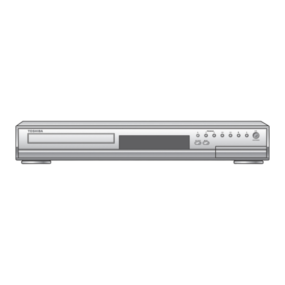
DVD Video Recorder
D-R265SE
The above model is classified as a green product (*1), as indicated by the underlined serial
number. This Service Manual describes replacement parts for the green product. When
repairing this green product, use the part(s) described in this manual and lead-free solder (*2).
For (*1) and (*2), see the next page.
TOSHIBA CORPORATION 2006
Published in Japan, May 2006 GREEN
Advertisement
Table of Contents

Related Manuals for Toshiba D-R265SE


Summary of Contents for Toshiba D-R265SE
- Page 1 This Service Manual describes replacement parts for the green product. When repairing this green product, use the part(s) described in this manual and lead-free solder (*2). For (*1) and (*2), see the next page. TOSHIBA CORPORATION 2006 Published in Japan, May 2006 GREEN...
- Page 2 Hazardous Substances. From July 1, 2006, the RoHS Directive will prohibit any marketing of new products containing the restricted substances. Increasing attention is given to issues related to the global environmental. Toshiba Corporation recognizes environmental protection as a key management tasks, and is doing its utmost to enhance and improve the quality and scope of its environmental activities.
-
Page 3: Table Of Contents
It also is important to understand that these CAUTIONS and NOTICES ARE NOT EXHAUSTIVE. TOSHIBA could not possibly know, evaluate and advice the service trade of all conceivable ways in which service might be done or of the possible hazardous consequences of each way. -
Page 4: Specifications
SPECIFICATIONS General Input/Output System Front Panel : (AV4) DVD-Video, DVD-R/RW, CD-DA, CD-R/RW, Video input One RCA connector Input level : 1Vp-p (75 Ω) Power requirements 220–240V ± 10%, 50Hz ± 0.5% S-Video input Power consumption One Mini DIN 4-pin jack Y (Iuminance) 1Vp-p (75 Ω) 25W (standby: 4.5W) Input level :... -
Page 5: Laser Beam Safety Precautions
LASER BEAM SAFETY PRECAUTIONS This DVD player uses a pickup that emits a laser beam. Do not look directly at the laser beam coming from the pickup or allow it to strike against your skin. The laser beam is emitted from the location shown in the figure. When checking the laser diode, be sure to keep your eyes at least 30 cm away from the pickup lens when the diode is turned on. -
Page 6: Important Safety Precautions
IMPORTANT SAFETY PRECAUTIONS Product Safety Notice K. Crimp type wire connector The power transformer uses crimp type connectors Some electrical and mechanical parts have special which connect the power cord and the primary side safety-related characteristics which are often not evi- of the transformer. - Page 7 Safety Check after Servicing Examine the area surrounding the repaired location for damage or deterioration. Observe that screws, Chassis or Secondary Conductor parts, and wires have been returned to their original positions. Afterwards, do the following tests and con- Primary Circuit firm the specified values to verify compliance with safety standards.
-
Page 8: Standard Notes For Servicing
STANDARD NOTES FOR SERVICING NOTE: BOARD MEANS PRINTED CIRCUIT BOARD. Circuit Board Indications Pb (Lead) Free Solder 1. The output pin of the 3 pin Regulator ICs is When soldering, be sure to use the Pb free solder. indicated as shown. How to Remove / Install Flat Pack-IC Top View Bottom View... - Page 9 With Soldering Iron: 3. The flat pack-IC on the BOARD is affixed with glue, so be careful not to break or damage the foil 1. Using desoldering braid, remove the solder from of each pin or the solder lands under the IC when all pins of the flat pack-IC.
- Page 10 2. Installation With Iron Wire: 1. Using desoldering braid, remove the solder from 1. Using desoldering braid, remove the solder from all pins of the flat pack-IC. When you use solder the foil of each pin of the flat pack-IC on the flux which is applied to all pins of the flat pack-IC, BOARD so you can install a replacement flat pack- you can remove it easily.
- Page 11 Instructions for Handling Semi- conductors Electrostatic breakdown of the semi-conductors may occur due to a potential difference caused by electrostatic charge during unpacking or repair work. 1. Ground for Human Body Be sure to wear a grounding band (1 MΩ) that is properly grounded to remove any static electricity that may be charged on the body.
-
Page 12: Cabinet Disassembly Instructions
CABINET DISASSEMBLY INSTRUCTIONS NOTE: BOARD MEANS PRINTED CIRCUIT BOARD. 1. Disassembly Flowchart Removal Remove/*Unhook/ Loc. Part This flowchart indicates the disassembly steps to gain Fig. Unlock/Release/ Note access to item(s) to be serviced. When reassembling, Unplug/Desolder follow the steps in reverse order. Bend, route, and dress the cables as they were originally. - Page 13 [8] FAN COVER (S-7) [2] PANEL FRONT FAN EARTH [9] FAN (L-1) [10] PANEL REAR (S-9) (S-10) (L-1) (S-8) (L-1) (L-2) Fig. D2 CN1601 Fig. D5 (S-2) (S-2) [3] DVD MECHANISM & DVD MAIN BOARD [13] BOARD AFV ASSEMBLY (S-11) [12] BOARD JACK CN101 (S-11)
- Page 14 3. How to Eject Manually Note: When rotating the gear, be careful not to damage the gear. 1. Remove the COVER TOP. 2. Rotate the gear in the direction of the arrow manually as shown below until the tray descends. 3.
-
Page 15: How To Initialize The Dvd Recorder
HOW TO INITIALIZE THE DVD RECORDER To put the program back at the factory-default, initialize the DVD recorder as the following procedure. 1. Turn the DVD recorder on. 2. Confirm that no disc is loaded or that the disc tray is open. -
Page 16: Firmware Renewal Mode
FIRMWARE RENEWAL MODE 1. Turn the power on and remove the disc on the tray. 4. Select the firmware version pressing arrow buttons, then press [ENTER]. 2. To put the DVD recorder into version up mode, Fig. d appears on the screen and Fig. e appears press [INSTANT SKIP], [6], [5], and [4] buttons on on the VFD. -
Page 17: Troubleshooting
TROUBLESHOOTING NOTE: BOARD MEANS PRINTED CIRCUIT BOARD. FLOW CHART NO.1 The power cannot be turned on. See FLOW CHART No.2 <The fuse blows out.> Is the fuse normal? Is normal state restored when once unplugged Check for lead or short-circuiting of primary power cord is plugged again after several seconds. - Page 18 FLOW CHART NO.6 P-ON+10V is not outputted. Check Q1160, D1162 and their periphery, and Is 12V voltage supplied to the collector of Q1160? service it if defective. Check D1102, D1113, C1117, L1102 and their Is 12V voltage supplied to the emitter of Q1155? periphery, and service it if defective.
- Page 19 FLOW CHART NO.12 EV+3.3V is not outputted. Check D1108, L1105, C1120 and their periphery, Is 5V voltage supplied to the collector of Q1159? and service it if defective. Is the voltage of approximately 4V supplied to Check IC1153 and their periphery, and service it if the base of Q1159? defective.
- Page 20 FLOW CHART NO.16 The key operation is not functioning. Are the contact point and the installation state of Re-install some key switches correctly or the key switches normal? replace some key switches. Check the key switches and their periphery, and Is the control voltage normally inputted into service it if defective.
- Page 21 FLOW CHART NO.19 [No Disc] indicated. Both functions of picture and sound do not operate normally. Replace the DVD MECHANISM & DVD MAIN BOARD ASSEMBLY. FLOW CHART NO.20 VIDEO E-E does not appear normally. Are the video signals inputted to each pin of Check the line between video input terminal and IC1201? each pin of IC1201.
- Page 22 Replace the DVD MECHANISM & DVD MAIN Are the video signals outputted to each pin of BOARD ASSEMBLY. CN1201 on the BOARD POWER? CN1201 24PIN VIDEO-Y(I/P)-OUT CN1201 30PIN VIDEO-Y(I)-OUT CN1201 26PIN VIDEO-Cr/Pr-OUT CN1201 28PIN VIDEO-Cb/Pb-OUT CN1201 22PIN VIDEO-C-OUT Are the video signals shown above inputted into Check the line between each pin of CN1201 and each pin of IC1201? each pin of IC1201, and service it if defective.
- Page 23 FLOW CHART NO.21 Picture does not appear normally. Set the disc on the disc tray, and playback. Replace the DVD MECHANISM & DVD MAIN Are the video signals outputted to each pin of BOARD ASSEMBLY. CN1201 on the BOARD POWER? CN1201 24PIN VIDEO-Y(I/P)-OUT...
- Page 24 FLOW CHART NO.22 Check the line between audio input terminal and Audio E-E does not appear normally. each pin of IC1201, and service it if defective. No (Rear →JK1206 IC1201 93,94PIN AUDIO-IN1 (AV1) or Front →JK1202, IC1201 91,92PIN AUDIO-IN1 (FRONT) input) Are the audio signals inputted to each pin of JK1203...
- Page 25 Replace the DVD MECHANISM & DVD MAIN Are the analog audio signals outputted to each pin BOARD ASSEMBLY. of CN1201 on BOARD POWER? CN1201 14PIN AUDIO (L)-OUT CN1201 16PIN AUDIO (R)-OUT Are the analog audio signals inputted to each pin Check each line between each pin of CN1201 and each pin of IC1202, and service it if defective.
- Page 26 FLOW CHART NO.23 Audio is not outputted during playback. Set the disc on the disc tray, and playback. Replace the DVD MECHANISM & DVD MAIN Are the analog audio signals outputted to each pin BOARD ASSEMBLY. of CN1201 on BOARD POWER? CN1201 14PIN AUDIO (L)-OUT CN1201 16PIN AUDIO (R)-OUT Check each line between each pin of CN1201...
-
Page 27: Function Indicator Symbols
FUNCTION INDICATOR SYMBOLS Note: If an error occurs, a message with the error number appears on the screen. Recording Error Error message You cannot record on this disc as Power Calibration Area is full. Error No. Error Message Solution Error Description Priority An error occurs during data reading. - Page 28 Error Message Solution Error Description Priority Release the disc protect This disc is protected and not setting in the Disc Setting Disc Protected Disc. recordable. menu. Disc is full. Insert the recordable disc with No avilable recording space. (No area for new recording) enough recording space.
-
Page 29: Lead Identifications
LEAD IDENTIFICATIONS KRC103M-AT/P 2SC1815-GR(TE2 F T) PQ070XF01SZH KTA-1266-GR-AT/P 2SC2001-T-A-K KTA1267-Y-AT/P KTC3203-Y-AT/P KTA1273-Y-AT/P KTC3266-GR-AT/P KTC3199-(BL,Y)-AT/P 1 2 3 4 E C B E C B KIA4558P/P EL817A BU4219G-TR SSM3K15F(TE85L F) 2SK3566 RC4580IP PST3619NR 1: A R3112N191A-TR-FA 2: K 3: E 4: C 1 2 3 G D S KIA431-AT/P... -
Page 30: Exploded Views
EXPLODED VIEWS NOTE: BOARD MEANS PRINTED CIRCUIT BOARD. Cabinet See Electrical Parts List for parts with this mark. 2B15 Some Ref. Numbers are 2L021 FM1001 not in sequence. 2L021 2L021 2L012 2L013 2L021 2L081 2L021 BOARD SWITCH ( P1 ) POWER ASSEMBLY 2L081 ( P2 ) - Page 31 Packing X10B X10A Some Ref. Numbers are not in sequence. X10C X10D Unit 1-17-2 E7B70PEX...
-
Page 32: Mechanical Parts List
MECHANICAL PARTS LIST PRODUCT SAFETY NOTE: Products marked with a ! have special characteristics important to safety. Before replacing any of these components, read carefully the product safety notice in this service manual. Don't degrade the safety of the product through improper servicing. -
Page 33: Electrical Parts List
ELECTRICAL PARTS LIST PRODUCT SAFETY NOTE: Products marked with a Location TSB P/N Reference No. Description ! have special characteristics important to safety. Before replacing any of these components, read C1176 CHD1JZ30F104 CHIP CERAMIC CAP .(1608) F Z 0.1µF/50V carefully the product safety notice in this service C1177 CHD1JZ30F104 CHIP CERAMIC CAP .(1608) F... - Page 34 Location Location TSB P/N Reference No. Description TSB P/N Reference No. Description C1245 CHD1JZ30F104 CHIP CERAMIC CAP .(1608) F C1287 CE1JMASDL1R0 ELECTROLYTIC CAP . 1µF/50V Z 0.1µF/50V C1246 CE1EMASDL4R7 ELECTROLYTIC CAP . 4.7µF/ C1288 CE0KMASDL471 ELECTROLYTIC CAP . 470µF/ 25V M 6.3V M C1247 CE1AMASDL470...
- Page 35 Location Location TSB P/N Reference No. Description TSB P/N Reference No. Description C1649 CE1JMASDL1R0 ELECTROLYTIC CAP . 1µF/50V D1160 NDTZ01N4148M SWITCHING DIODE 1N4148M D1162 NDTB00DZ11BS ZENER DIODE DZ- C1650 CHD1JK30B103 CHIP CERAMIC CAP .(1608) B 11BSBT265 K 0.01µF/50V D1163 NDTB0DZ5R6BS ZENER DIODE DZ- C1651 CE0KMASDL470 ELECTROLYTIC CAP .
- Page 36 Location Location TSB P/N Reference No. Description TSB P/N Reference No. Description L1501 LLAXKATTU101 INDUCTOR(100µH K) Q1813 NQSYKTC3199P TRANSISTOR KTC3199-Y-AT/ LAP02TA101K L1502 LLAXKATTU101 INDUCTOR(100µH K) Q1814 NQSYKTC3199P TRANSISTOR KTC3199-Y-AT/ LAP02TA101K RESISTORS L1703 LLAXKATTU100 INDUCTOR 10µH-K-26T CHIP RES.(1608) 1/10W 0 Ω L1801 LLAXKATTU101 INDUCTOR(100µH K)
- Page 37 Location Location TSB P/N Reference No. Description TSB P/N Reference No. Description CHIP RES. 1/10W F 13k Ω R1230 RRXAFR5H1302 R1565 JW5.0T BOARD JUMPER D0.6-P5.0 CHIP RES. 1/10W J 13k Ω CARBON RES. 1/4W J 560 Ω R1231 RRXAJR5Z0133 R1566 RCX4JATZ0561 CHIP RES.
- Page 38 Location Location TSB P/N Reference No. Description TSB P/N Reference No. Description CHIP RES. 1/10W J 220 Ω R1850 RRXAJR5Z0221 SW3005 P000460010 SST0101HH003 TACT SWITCH KSM0612B CHIP RES. 1/10W J 220 Ω R1851 RRXAJR5Z0221 SW3006 P000460010 SST0101HH003 TACT SWITCH KSM0612B CHIP RES.
- Page 39 Location Location TSB P/N Reference No. Description TSB P/N Reference No. Description CARBON RES. 1/6W J 5.6k Ω D1005 NDTZ01N4148M SWITCHING DIODE 1N4148M R1017 RCX6JATZ0562 CARBON RES. 1/4W J 1k Ω D1006 NDTZ01N4148M SWITCHING DIODE 1N4148M R1018 RCX4JATZ0102 D1007 NDTZ01N4148M SWITCHING DIODE 1N4148M R1019 RN02823ZU001...
- Page 40 Location Location TSB P/N Reference No. Description TSB P/N Reference No. Description D2002 NDTA00DZ11BS ZENER DIODE DZ-11BSAT265 CHD1JZ30F104 CHIP CERAMIC CAP .(1608) F Z 0.1µF/50V D2003 NDTA00DZ11BS ZENER DIODE DZ-11BSAT265 CHD1JZ30F104 CHIP CERAMIC CAP .(1608) F Z D2004 NDTA00DZ11BS ZENER DIODE DZ-11BSAT265 0.1µF/50V D2005 NDTA00DZ11BS...