Samsung YP-S2 Service Manual
Hide thumbs
Also See for YP-S2:
- User manual (38 pages) ,
- User manual (38 pages) ,
- User manual (33 pages)
Table of Contents
Advertisement
Quick Links
SERVICE
YEPP
YP-S2
Refer to the service manual in the GSPN (see the rear cover) for the more information.
YEPP
Model Name : YP-S2
Model Code : YP-S2ZW/EDC
YP-S2ZW/XSP
Manual
1. Precaution
2. Product Specification
3. Disassembly & Reassembly
4. Troubleshooting
5. Exploded View & Part List
6. PCB Diagram
7. Schematic Diagram
CONTENTS
Advertisement
Table of Contents

Related Manuals for Samsung YP-S2


Summary of Contents for Samsung YP-S2
- Page 1 YEPP Model Name : YP-S2 Model Code : YP-S2ZW/EDC YP-S2ZW/XSP SERVICE Manual YEPP CONTENTS 1. Precaution 2. Product Specification 3. Disassembly & Reassembly 4. Troubleshooting 5. Exploded View & Part List 6. PCB Diagram 7. Schematic Diagram YP-S2 Refer to the service manual in the GSPN (see the rear cover) for the more information.
- Page 2 Asia asia.samsungportal.com Mideast & Africa mea.samsungportal.com © Samsung Electronics Co.,Ltd. May. 2008 This Service Manual is a property of Samsung Electronics Printed in Korea Co.,Ltd. Any unauthorized use of Manual can be punished under applicable International and/or domestic law.
-
Page 3: Table Of Contents
Contents 1. Precaution 1-1 Safety Precautions .................... 1-1 1-2 Static Electricity Precautions ................1-2 2. Product Specification 2-1 Product Feature ....................2-1 2-2 Specifications ....................2-2 2-3 Specifications Analysis ..................2-3 2-4 Accessories .......................2-5 3. Disassembly & Reassembly 3-1 Overall Disassembly & Reassembly ..............3-1 4. -
Page 4: Precaution
5. You should not put any object or liquid into product. Otherwise, it may cause failure or mal-operation. 6. If replacement material is required, service engineer should use materials with the same standard. The use of non-standardized materials may cause failure of product. Samsung Electronics... -
Page 5: Static Electricity Precautions
4. Minimize physical operation when handling with the ESD device for replacement without packing (Otherwise, namely friction between cloth fibers or lifting of the foot from the carpet floor may cause static electricity enough to damage the ESD device). Samsung Electronics... -
Page 6: Product Specification
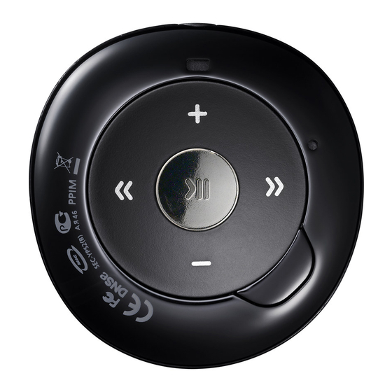
+/- Button Smart Button button’s Long- key - Audio change feature using the Smart button’s Short- key (Normal - Concert Hall - Club) - Replay mode using the Smart button’s Long- key (Normal (Blue) - Shuffle (Green-Blue-Purple) - Playlist (Purple)) Samsung Electronics... -
Page 7: Specifications
Product Specification 2-2 Specifications Basic Specification YP-S2 Model Name Capacity Color Black White Green Purple Black White Green Purple Voltage 3.7V Dimensions (WxDxH) 16.6 x 41.15 x 42.385 mm / 16.2g / Weight Noise Ratio 90dB with A filter Earphone Output 16mW (16mW x 16mW, 16Ω) -
Page 8: Specifications Analysis
Product Specification 2-3 Specifications Analysis YP-S2 YP-U3 Model Name Photo Storage TYPE Flash memory (MLC) Flash memory (MLC) Display X (LED Display) 1 inch OLED Platform Serenade (144pin) Serenade (POP) Battery Li-Polymer Li-Polymer Basic Battery Capacity 200mAh 250mAh Playback Time 13hrs 15hrs (Earphone) Color Black/Red/Purple/Green/White... - Page 9 Product Specification YP-S2 YP-U3 Model Name Photo Tuner Etc. Voice Recording Voice Recording Recording Format Function Recording Mode 4 Mode (32Kbps ~128Kbps) Playlist Mobile Playlist (Favorite) Mobile Playlist (Favorite) PC Playlist (SPL, WPL) Function Folder play (Browse) (Music) Library (Artist, Album, Genre, Title DB sorting) File Navigation ...
-
Page 10: Accessories
Product Specification 2-4 Accessories 2-4-1 Supplied Accessories Accessories Item Item code Remark AH30-00105A Earphones Direct Connect USB 3722-002740 Samsung Service center Adaptor AH46-00059A Program Installation CD Samsung Electronics... - Page 11 MEMO Samsung Electronics...
-
Page 12: Disassembly & Reassembly
1) Remove the LED silicone from the COVER open machine. LENS FRAME-A 1) Remove 2 screws from FRAME-A. : CH,+,B,M1.7,L4,ZPC(BLK) BATTERY 1) Use the pin set to remove the connector connected to the MAIN PCB and remove the BATTERY. Samsung Electronics... - Page 13 Disassembly & Reassembly Part Name Description Description Photo MAIN PCB 1) Remove the MAIN PCB from the CABINET-BACK. CABINET- 1) Remove the CABINET-BACK and BACK KEY PAD. KEY PAD 2) How the SET looks when completely dismantled. Samsung Electronics...
-
Page 14: Troubleshooting
Troubleshooting 4. Troubleshooting 4-1 Checkpoints by Error Mode ..............4-2 4-2 Upgrade Methods .................4-16 Samsung Electronics... -
Page 15: Checkpoints By Error Mode
32.768KHz there a Short?) Refer to wave pattern image of Fig. 4-3. Is the RTC Replace malfunctioning voltage applied? MAIN IC board R37 → 3.3V Refer to wave pattern image of Fig. 4-4. Finished Samsung Electronics... - Page 16 PC? If you press the Play key and the DNSE key (replay Update DFU firmware and mode) at the same time and recheck connect the USB, is it recognized as a DFU device? Replace BOARD (Requires close inspection) Samsung Electronics...
- Page 17 Troubleshooting MAIN Page, 7-3 IC11 PCB Bottom Page, 6-4 <Fig. 4-1> Samsung Electronics...
- Page 18 Troubleshooting MAIN Page, 7-3 PCB Bottom Page, 6-4 <Fig. 4-2> Samsung Electronics...
- Page 19 Troubleshooting MAIN Page, 7-3 PCB Bottom Page, 6-4 <Fig. 4-3> Samsung Electronics...
- Page 20 Troubleshooting MAIN Page, 7-3 PCB Top Page, 6-2 <Fig. 4-4> Samsung Electronics...
- Page 21 Troubleshooting MAIN Page, 7-3 PCB Bottom Page, 6-4 <Fig. 4-5> Samsung Electronics...
- Page 22 Does the R/L-CH come out normally? Can audio stoppage or interference be heard? Can it be heard when playing other files? Do the symptoms appear even after upgrading to the latest firmware? Replace BOARD (Requires close inspection) Finished Samsung Electronics...
- Page 23 DFU Check for short in ‘My Computer’? Update? Pin1 and R14 Short Is formatting Is there ACCESS? occurring in Windows Explorer? Add solder then connect USB and recheck Finished Connect USB MAIN IC malfunction (replace Board) 4-10 Samsung Electronics...
- Page 24 Troubleshooting MAIN Page, 7-3 PCB Bottom Page, 6-4 <Fig. 4-6> Samsung Electronics 4-11...
- Page 25 Is the red LED Does the red not turn on? TR/resistance cold soldered? (R1, Q1) Refer to wave pattern Add solder to red LED image of Fig. 4-7. element and recheck Replace BOARD (Requires close inspection) 4-12 Samsung Electronics...
- Page 26 Troubleshooting MAIN Page, 7-3 PCB Bottom Page, 6-4 PCB Top Page, 6-2 <Fig. 4-7> Samsung Electronics 4-13...
- Page 27 (Vol+, Vol-, FF, REW: R32, DNSe: R34, START: R35, R37) Refer to wave pattern image of Fig. 4-8. Replace BOARD Add solder to Pull Up (Requires close inspection) resistance and recheck Replace the button device and recheck 4-14 Samsung Electronics...
- Page 28 Troubleshooting MAIN Page, 7-3 PCB Bottom Page, 6-4 <Fig. 4-8> Samsung Electronics 4-15...
-
Page 29: Upgrade Methods
- Files are corrupted, or the product shows as a “removable storage” in Windows but cannot be accessed. 4-2-1 Firmware Upgrade Method 1. Put the latest firmware [YP-S2.ROM and YP-S2.SET] on the portable disk (root). 2. Turn on the power and the update will run. - Page 30 Troubleshooting 4-2-2 Bootloader Upgrade Method When do you perform this procedure?: When NAND data is corrupted How to install YP-S2 as DFU DEVICE 1. Hold down the Smart key and press Play and connect the USB. - The LED on the set will turn a pale blue (green+blue). - After DFU connection, the POWER KEY can be released.
- Page 31 1 In the New_DFU_Program folder, go to the Image folder and select S5L8424_UpdaterBE_0142_ 080125Chk.DFU 2 In the YP-S2 firmware folder select YP-S2.BIN 3 Press F/W Upgrade. If the Browse button is inactive, there is no DFU connection and you must pull out the USB and try again.
-
Page 32: Exploded View & Part List
Exploded View & Part List 5. Exploded View & Part List 5-1 Exploded View ..................5-2 5-2 Electrical Part List ................5-4 Samsung Electronics This Document can not be used without Samsung’s authorization. -
Page 33: Exploded View
Exploded View & Part List 5-1 Exploded View AC000 AF001 AR062 AC010 AA145 AS040 This Document can not be used without Samsung’s authorization. Samsung Electronics... - Page 34 AC000 AH64-04666B CABINET-BACK;YP-S2,PC,T1.2,W42.0,L42.45, AC010 AH64-04665B CABINET-FRONT;YP-S2,PC,T1.2,W42.0,L42.45 AF001 AH61-02616A FRAME-A;YP-S2,ABS,-,-,BLACK,T1.6,W37.7 AR062 AH73-00145A RUBBER-LIGHT;YP-S2,SILICON,30,60,40,TRAN AS040 6003-001292 SCREW-TAPTITE;CH(0.3),+,B,M1.7,L3,ZPC(BL BATTERY AH43-00017A SOFT BATTERY PACK;-,YP-S2,Soft Pack(Li-P PCB-MAIN AH92-02877B ASSY PCB-MAIN;S2 MAIN PCB,1GB, White Ear Samsung Electronics This Document can not be used without Samsung’s authorization.
-
Page 35: Electrical Part List
3710-001105 SOCKET-BOARD TO BOARD;2P,1R,1.27mm, VAR2 1405-001093 VARISTOR;14V,20A,1x0.5x0.6mm,TP 0406-001239 DIODE-TVS;RClamp0502B,6V,125W,SOT-5 VOL- 3404-001121 SWITCH-TACT;12V DC,50mA,160gf,4.8x4 0404-001089 DIODE-SCHOTTKY;RB551V-30,20V,500MA, VOL+ 3404-001121 SWITCH-TACT;12V DC,50mA,160gf,4.8x4 DNSe 3404-001121 SWITCH-TACT;12V DC,50mA,160gf,4.8x4 3404-001121 SWITCH-TACT;12V DC,50mA,160gf,4.8x4 X-TAL1 2801-000102 CRYSTAL-SMD;12MHz,30ppm,-,12pF,100o X-TAL2 2801-004339 CRYSTAL-SMD;0.032768MHZ,20PPM,SMD,9 IC11 1107-001661 IC-FLASH MEMORY;K9G8G08U0M,8Gbit,1G This Document can not be used without Samsung’s authorization. Samsung Electronics... - Page 36 SNA XSP AH69-02201A PACKING-CASE-BOTTOM;YP-T10,PC,-,2,8 SNA AH63-01455A SHEET-CASE;YP-U3,PET,T0.1,W20,L8,-, SNA AH68-00508U LABEL SERIAL;COMMON,ELS,-,-,90,-,-, 0.1 SNA AH68-02087C LABEL-ORIGIN;YP-S2,XAA,art paper,-, SNA EDC AH68-02087B LABEL-ORIGIN;YP-S2,XTL,art paper,-, SNA XSP AH68-50119B LABEL-EAN(B);ART-PAPER,T0.05,L29,W4 1.05 SNA AH69-02211E MASTER CARTON;YP-S2/ELS,OTHER,T7,W3 0.1 SNA AH69-02212C CARTON-PAD ASSY;YP-S2/ELS,OTHER,T7, 0.1 SNA Samsung Electronics This Document can not be used without Samsung’s authorization.
- Page 37 MEMO Samsung Electronics...
-
Page 38: Pcb Diagram
PCB Diagram 6. PCB Diagram 6-1 PCB Top ......................6-2 6-2 PCB Bottom ...................... 6-4 Samsung Electronics... -
Page 39: Pcb Top
PCB Diagram 6-1 PCB Top 24MHz Crystal Samsung Electronics... - Page 40 PCB Diagram 6-1-1 Test Point Wave Form Samsung Electronics...
-
Page 41: Pcb Bottom
PCB Diagram 6-2 PCB Bottom IC11 Earphone Jack Switch IC Battery Connector Nand 32.768KHz Crystal Main DSP Samsung Electronics... - Page 42 PCB Diagram 6-2-1 Pin Connection 6-2-2 Test Point Wave Form 1 JACK2 3 CON1 Earphone Jack Battery Connector Pin No. Signal Pin No. Signal R-CH, USB_DP VBAT L-CH, USB_DM GROUND V-BUS (5V) GROUND Samsung Electronics...
- Page 43 MEMO Samsung Electronics...
-
Page 44: Schematic Diagram
Schematic Diagram 7. Schematic Diagram 7-1 Overall Block Diagram ..................7-2 7-2 MAIN ........................7-3 Samsung Electronics This Document can not be used without Samsung’s authorization. -
Page 45: Overall Block Diagram
- 2 CH PMU (1.2V, 3.0V) Memory Interface CODEC Earphone Audio_R/L USB+, USB- SDRAM (5M) VBUS 5V Controller +ROM (50k) JACK VIO_3.0 USB CLK Main CLK 12 Mhz 32.768 Khz Key Input (Tact SW) This Document can not be used without Samsung’s authorization. Samsung Electronics... -
Page 46: Main
Schematic Diagram 7-2 MAIN POWER AUDIO Samsung Electronics This Document can not be used without Samsung’s authorization. - Page 47 MEMO Samsung Electronics...