Table of Contents

Related Manuals for Aaeon PCM-8120


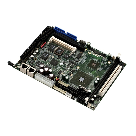
Summary of Contents for Aaeon PCM-8120
- Page 1 P C M - 8 1 2 0 PCM-8120 VIA C7/ Eden Series Processors One DDR 400/533 DDRII DIMM 48-bit Dual-Channel LVDS TFT LCD 7.1CH High Definition Audio 6 USB 2.0 / 4 COMs / Digital IO PCM-8120 Manual Rev.A 2nd Ed. Oct. 2008...
-
Page 2: Copyright Notice
AAEON assumes no liabilities resulting from errors or omissions in this document, or from the use of the information contained herein. AAEON reserves the right to make changes in the product design without notice to its users. - Page 3 C o m p a c t B o a r d P C M - 8 1 2 0 Acknowledgments All other products’ name or trademarks are properties of their respective owners. Award is a trademark of Award Software International, Inc. CompactFlash™...
-
Page 4: Packing List
Before you begin installing your card, please make sure that the following materials have been shipped: • 1 9657666600 Jumper Cap • 1 PCM-8120 CPU Card • 1 Quick Installation Guide • 1 CD-ROM for manual (in PDF format) and drivers If any of these items should be missing or damaged, please contact your distributor or sales representative immediately. -
Page 5: Table Of Contents
C o m p a c t B o a r d P C M - 8 1 2 0 Contents Chapter 1 General Information 1.1 Introduction..............1-2 1.2 Features ..............1-3 1.3 Specifications ............1-4 Chapter 2 Quick Installation Guide 2.1 Safety Precautions ............ - Page 6 C o m p a c t B o a r d P C M - 8 1 2 0 2.18 TV_Out Connector (CN1)........2-14 2.19 TTL_LCD Connector (CN2) ........2-15 2.20 INVERTER (CN3)............ 2-16 2.21 VGA Display Connector (CN4)........ 2-16 2.22 ATX Power Connector (CN5)........
- Page 7 C o m p a c t B o a r d P C M - 8 1 2 0 2.43 Floppy Connector (FDD1) ........2-27 2.44 IDE Connector (IDE1) ........... 2-28 2.45 LPT Port Connector (LPT1) ........2-29 Chapter 3 Award BIOS Setup 3.1 System Test and Initialization.
-
Page 8: Chapter 1 General Information
C o m p a c t B o a r d P C M - 8 1 2 0 Chapter General Information 1- 1 Chapter 1 General Information... -
Page 9: Introduction
Compact Board can easily adapt to diverse applications in this competitive industrial embedded market. PCM-8120 adopts a VIA C7 processor which features low power consumption and transcendent performance. In addition to the VIA C7 processor from 1GHz to 2GHz, this model can be equipped with an Eden V4 Bus (400MHz to 1.5GHz) processor. -
Page 10: Features
C o m p a c t B o a r d P C M - 8 1 2 0 1.2 Features Onboard VIA C7/ Eden (V4 Bus) series processors One DIMM DDR II 400/533 up to 1GB Dual-channel LVDS, DVI and TV-out MPEG-4 accelerator Dual 10/100Base-TX Ethernet PCI, Type III Mini PCI, PC/104 &... -
Page 11: Specifications
C o m p a c t B o a r d P C M - 8 1 2 0 1.3 Specifications System Supports VIA C7/ Eden (V4 Bus) series processors up to 2.0GHz with FSB 400/ 533MHz (only C7 1.8G &... - Page 12 C o m p a c t B o a r d P C M - 8 1 2 0 Power Requirement AT/ ATX Operating Temperature F~140 F (0 C~60 Board Size 8”(L) x5.72” (W) (203mm x 146mm) Gross Weight 1.2 lb (0.5kg) Display: Support: CRT/LVDS, LVDS/TV or CRT/TTL, CRT/DVI, TV/TTL, TV/DVI simultaneous/ dual view displays.
- Page 13 C o m p a c t B o a r d P C M - 8 1 2 0 Mouse x 1, Parallel x 1 (supports SPP/ EPP/ ECP mode), RS-232 x 3, RS-232/422/485 x 1 IDE Interface P-ATA-133 x 1 channel, SATA II x 2 with RAID 0 &...
-
Page 14: Chapter 2 Quick Installation Guide
C o m p a c t B o a r d P C M - 8 1 2 0 Chapter Quick Installation Guide Notice: The Quick Installation Guide is derived from Chapter 2 of user manual. For other chapters further installation instructions, please refer to the user... -
Page 15: Safety Precautions
C o m p a c t B o a r d P C M - 8 1 2 0 2.1 Safety Precautions Always completely disconnect the power cord from your board whenever you are working on it. Do not make connections while the power is on, because a sudden rush of power can damage sensitive electronic components. -
Page 16: Location Of Connectors And Jumpers
C o m p a c t B o a r d P C M - 8 1 2 0 2.2 Location of Connectors and Jumpers Component Side 2- 3 Chapter 2 Quick Installation Guide... - Page 17 C o m p a c t B o a r d P C M - 8 1 2 0 Solder Side 2 - 4 Chapter 2 Quick Installation Guide...
-
Page 18: Mechanical Drawing
C o m p a c t B o a r d P C M - 8 1 2 0 2.3 Mechanical Drawing Component Side (Passive) 139.27 138.51 140.97 137.53 135.89 135.89 134.62 133.10 134.11 130.81 127.89 129.78 135.89 126.84 122.68 135.64 127.51... - Page 19 C o m p a c t B o a r d P C M - 8 1 2 0 Component Side (Active) 139.27 138.51 140.97 137.53 135.89 135.89 134.62 133.10 134.11 130.81 129.78 127.89 135.89 126.84 122.68 135.64 127.51 117.60 116.11 114.81...
- Page 20 C o m p a c t B o a r d P C M - 8 1 2 0 Solder Side 140.97 135.89 135.89 135.89 126.84 119.99 95.88 68.74 63.25 58.10 22.47 13.25 10.16 0.00 0.00 0.00 0.00 2- 7 Chapter 2 Quick Installation Guide...
-
Page 21: List Of Jumpers
C o m p a c t B o a r d P C M - 8 1 2 0 2.4 List of Jumpers The board has a number of jumpers that allow you to configure your system to suit your application. The table below shows the function of each of the board's jumpers: Jumpers Label... -
Page 22: List Of Connectors
C o m p a c t B o a r d P C M - 8 1 2 0 2.5 List of Connectors The board has a number of connectors that allow you to configure your system to suit your application. The table below shows the function of each board's connectors: Connectors Label... - Page 23 C o m p a c t B o a r d P C M - 8 1 2 0 CN18 AT Power Connector (Optional) CN19 SATA1 Connector CN20 SATA2 Connector CN22 Audio 5.1 Channel/SPDIF Connector CN23 USB3 Connector CN24 First Digital I/O Connector CN25 Second Digital I/O Connector...
-
Page 24: Setting Jumpers
C o m p a c t B o a r d P C M - 8 1 2 0 2.6 Setting Jumpers You configure your card to match the needs of your application by setting jumpers. A jumper is the simplest kind of electric switch. It consists of two metal pins and a small metal clip (often protected by a plastic cover) that slides over the pins to connect them. -
Page 25: Audio Out Selection (Jp1)
C o m p a c t B o a r d P C M - 8 1 2 0 2.7 Audio Out Selection (JP1) Function 1-3, 2-4 W/O Amplifier 3-5, 4-6 W/ Amplifier (Default) 2.8 LVDS/DVI/ INVERTER Voltage Selection (JP2) For LVDS/DVI Function +3.3V (Default) -
Page 26: Clear Cmos (Jp4)
C o m p a c t B o a r d P C M - 8 1 2 0 2.10 Clear CMOS (JP4) Function Protected (Default) Clear 2.11 COM2 Ring/+5V/+12V Selection (JP5) Function +12V Ring (Default) 2.12 COM4 Ring/+5V/+12V Selection (JP6) Function +12V Ring (Default) -
Page 27: Com1 Ring/+5V/+12V Selection (Jp8)
C o m p a c t B o a r d P C M - 8 1 2 0 2.14 COM1 Ring/+5V/+12V Selection (JP8) Function +12V Ring (Default) 2.15 ATX/ AT Selection (JP9) Function ATX (Default) 2.16 TV/CRT Selection (JP10) JP10 Function CRT (Default) -
Page 28: Ttl_Lcd Connector (Cn2)
C o m p a c t B o a r d P C M - 8 1 2 0 N.C. N.C. 2.19 TTL_LCD Connector (CN2) Signal Signal +3.3V +3.3V ENBKL BLUE0 BLUE1 BLUE2 BLUE3 BLUE4 BLUE5 BLUE6 BLUE7 GREEN0 GREEN1 GREEN2 GREEN3... -
Page 29: Inverter (Cn3)
C o m p a c t B o a r d P C M - 8 1 2 0 HSYNC N.C. N.C. 2.20 INVERTER (CN3) Signal INV_VCC INV_VCC ENBKL N.C. 2.21 VGA Display Connector (CN4) Signal Signal GREEN BLUE DDCDAT HSYNC VSYNC... -
Page 30: Atx Power Connector (Cn5)
C o m p a c t B o a r d P C M - 8 1 2 0 2.22 ATX Power Connector (CN5) Signal Signal +3.3V +3.3V +3.3V -12V PS_ON POWER OK +5VSB +12V 2.23 Fan Connector (CN6) Signal +12V or +5V Speed Sense... - Page 31 C o m p a c t B o a r d P C M - 8 1 2 0 PPVCC LVDS1_TXCLK- LVDS1_TXCLK+ PPVCC LVDS1_TX0- LVDS1_TX0+ LVDS1_TX1- LVDS1_TX1+ LVDS1_TX2- LVDS1_TX2+ LVDS1_TX3- LVDS1_TX3+ N.C. N.C. LVDS2_TX0- LVDS2_TX0+ LVDS2_TX1- LVDS2_TX1+ LVDS2_TX2- LVDS2_TX2+ LVDS2_TX3- LVDS2_TX3+ PPVCC...
-
Page 32: Lan1 Led Connector (Cn8)
C o m p a c t B o a r d P C M - 8 1 2 0 DVI_SPCLK DVI_SPD N.C. N.C. N.C. N.C. N.C. N.C. N.C. N.C. PPVCC N.C. N.C. 2.25 LAN1 LED Connector (CN8) Signal Signal +3.3V Active LED Speed LED(100) -
Page 33: Com1~ Com4 Ports Connector (Cn11)
C o m p a c t B o a r d P C M - 8 1 2 0 2.27 COM1~COM4 Ports Connector (CN 11) Signal Signal DCD1 DSR1 RXD1 RTS1 TXD1 CTS1 DTR1 RI1/+5V/+12V COMGND N.C. DCD2(422TXD-/485DATA-) 12 DSR2 RXD2(422RXD+) RTS2... -
Page 34: Usb Connector (Cn12)
C o m p a c t B o a r d P C M - 8 1 2 0 2.28 USB Connector (CN12) Signal Signal USBD0- USBD0+ USBD1+ USBD1- 2.29 USB Connector (CN13) Signal Signal USBD2- USBD2+ USBD3+ USBD3- 2.30 IrDA Connector (CN14) Signal IRRX... -
Page 35: Fan Connector (Cn15)
C o m p a c t B o a r d P C M - 8 1 2 0 2.31 Fan Connector (CN15) Signal +12V or +5V Speed Sense 2.32 PS2 Keyboard/Mouse Connector (CN16) Signal Signal KB_DATA KB_CLK MS-DATA MS_CLK N.C. -
Page 36: Sata Connector (Cn19)
C o m p a c t B o a r d P C M - 8 1 2 0 +12V -12V 2.35 SATA Connector (CN19) Signal STXP_1 STXN_1 SRXN_1 SRXP_1 2- 23 Chapter 2 Quick Installation Guide... -
Page 37: Sata Connector (Cn20)
C o m p a c t B o a r d P C M - 8 1 2 0 2.36 SATA Connector (CN20) Signal STXP_2 STXN_2 SRXN_2 SRXP_2 2.37 Audio 5.1 Channel/SPDIF Connector (CN22) Signal Signal SIDE SURROUND_R SIDE SURROUND_L SURROUND_R SURROUND_L SENTER... -
Page 38: Usb Connector (Cn23)
C o m p a c t B o a r d P C M - 8 1 2 0 2.38 USB Connector (CN23) Signal Signal USBD4- USBD4+ USBD5+ USBD5- 2.39 First Digital I/O Connector (CN24) Signal Signal OUT1 OUT2 OUT3 OUT4 DIO Address is 800H... -
Page 39: Second Digital I/O Connector (Cn25)
C o m p a c t B o a r d P C M - 8 1 2 0 Port 2 CN24. pin 6 Bit 2 U26. pin 33 (GPIO12) Port 1 CN24. pin 7 Bit 1 U26. pin 34 (GPIO11) Port 0 CN24. -
Page 40: 10/100Base-Tx Ethernet Connector (Lan1)
C o m p a c t B o a r d P C M - 8 1 2 0 2.41 10/100 Base-TX Ethernet Connector (LAN1) Signal Signal Temp_GND Temp_GND Temp_GND Temp_GND Chassis_GND Chassis_GND 2.42 10/100 Base-TX Ethernet Connector (LAN2) Signal Signal Temp_GND... -
Page 41: Ide Connector (Ide1)
C o m p a c t B o a r d P C M - 8 1 2 0 #DRIVE SELECT B #DRIVE SELECT A #MOTOR B #DIR #STEP #WRITE DATA #WRITE GATE #TRACK0 #WRITE PROTECT #READ DATA #SIDE1 #DISK CHANGE 2.44 IDE Connector (IDE1) Signal... -
Page 42: Lpt Port Connector (Lpt1)
C o m p a c t B o a r d P C M - 8 1 2 0 N.C. IO WRITE IO READ IO READY DACK IRQ15 N.C. ADDR1 UDMA DETECT ADDR0 ADDR2 CS#1 CS#3 2.45 LPT Port Connector (LPT1) Signal Signal #STROBE... - Page 43 C o m p a c t B o a r d P C M - 8 1 2 0 BUSY SELECT N.C. 2 - 30 Chapter 2 Quick Installation Guide...
- Page 44 C o m p a c t B o a r d P C M - 8 1 2 0 Below Table for China RoHS Requirements 产品中有毒有害物质或元素名称及含量 AAEON Main Board/ Daughter Board/ Backplane 有毒有害物质或元素 部件名称 铅 汞 镉 六价铬 多溴联苯...
-
Page 45: Chapter 3 Award Bios Setup
C o m p a c t B o a r d P C M - 8 1 2 0 Chapter Award BIOS Setup Chapter 3 Award BIOS Setup 3-1... - Page 46 3. The CMOS memory has lost power and the configuration information has been erased. The PCM-8120 CMOS memory has an integral lithium battery backup for data retention. However, you will need to replace the complete unit when it finally runs down.
- Page 47 C o m p a c t B o a r d P C M - 8 1 2 0 3.2 Award BIOS Setup Awards BIOS ROM has a built-in Setup program that allows users to modify the basic system configuration. This type of information is stored in battery-backed CMOS RAM so that it retains the Setup information when the power is turned off.
- Page 48 Save CMOS value changes to CMOS and exit setup. Exit Without Saving Abandon all CMOS value changes and exit setup. You can refer to the "AAEON BIOS Item Description.pdf" file in the CD for the meaning of each setting in this chapter.
-
Page 49: Chapter 4 Driver Installation
C o m p a c t B o a r d P C M - 8 1 2 0 Chapter Driver Installation Chapter 4 Driver Installation... - Page 50 C o m p a c t B o a r d P C M - 8 1 2 0 The PCM-8120 comes with an AutoRun CD-ROM that contains all drivers and utilities that can help you to install the driver automatically.
- Page 51 C o m p a c t B o a r d P C M - 8 1 2 0 4.1 Installation: Insert the PCM-8120 CD-ROM into the CD-ROM drive and install the drivers from Step 1 to Step 5 in order. (Step 6 will be optional).
- Page 52 C o m p a c t B o a r d P C M - 8 1 2 0 4. The system will help you install the driver automatically Step 4 –Install Audio Driver 1. Click on the Step 4 –Audio folder and select the folder of Windows Driver 2.
- Page 53 C o m p a c t B o a r d P C M - 8 1 2 0 15. Click on Finish. Step 6 –Install RAID Driver (Optional) 1. Click on the Step 6 –RAID (optional) folder and double click on SETUP.exe 2.
-
Page 54: Appendix A Programming The Watchdog Timer
C o m p a c t B o a r d P C M - 8 1 2 0 Appendix Programming the Watchdog Timer Appendix A Programming the Watchdog Timer... -
Page 55: Programming
C o m p a c t B o a r d P C M - 8 1 2 0 A.1 Programming PCM-8120 utilizes ITE 8712 chipset as its watchdog timer controller. Below are the procedures to complete its configuration and the... - Page 56 C o m p a c t B o a r d P C M - 8 1 2 0 registers; (3) Exit the MB PnP Mode. Undesired result may occur if the MB PnP Mode is not exited normally. (1) Enter the MB PnP Mode To enter the MB PnP Mode, four special I/O write operations are to be performed during Wait for Key state.
- Page 57 C o m p a c t B o a r d P C M - 8 1 2 0 WatchDog Timer Configuration Registers Configure Control (Index=02h) This register is write only. Its values are not sticky; that is to say, a hardware reset will automatically clear the bits, and does not require the software to clear them.
- Page 58 C o m p a c t B o a r d P C M - 8 1 2 0 WatchDog Timer Control Register (Index=71h, Default=00h) WatchDog Timer Configuration Register (Index=72h, Default=00h) WatchDog Timer Time-out Value Register (Index=73h, Default=00h) Appendix A Programming the Watchdog Timer...
- Page 59 C o m p a c t B o a r d P C M - 8 1 2 0 A.2 IT8712 Watchdog Timer Initial Program .MODEL SMALL .CODE Main: CALL Enter_Configuration_mode CALL Check_Chip mov cl, 7 call Set_Logic_Device ;time setting mov cl, 10 ;...
- Page 60 C o m p a c t B o a r d P C M - 8 1 2 0 ; game port enable mov cl, 9 call Set_Logic_Device Initial_OK: CALL Exit_Configuration_mode MOV AH,4Ch INT 21h Enter_Configuration_Mode PROC NEAR MOV SI,WORD PTR CS:[Offset Cfg_Port] MOV DX,02Eh MOV CX,04h Init_1:...
- Page 61 C o m p a c t B o a r d P C M - 8 1 2 0 Exit_Configuration_Mode ENDP Check_Chip PROC NEAR MOV AL,20h CALL Read_Configuration_Data CMP AL,87h JNE Not_Initial MOV AL,21h CALL Read_Configuration_Data CMP AL,12h JNE Not_Initial Need_Initial: Not_Initial: Check_Chip ENDP...
- Page 62 C o m p a c t B o a r d P C M - 8 1 2 0 MOV DX,WORD PTR CS:[Cfg_Port+06h] IN AL,DX Read_Configuration_Data ENDP Write_Configuration_Data PROC NEAR MOV DX,WORD PTR CS:[Cfg_Port+04h] OUT DX,AL XCHG AL,AH MOV DX,WORD PTR CS:[Cfg_Port+06h] OUT DX,AL Write_Configuration_Data ENDP Superio_Set_Reg proc near...
- Page 63 C o m p a c t B o a r d P C M - 8 1 2 0 push ax push cx xchg al,cl mov cl,07h call Superio_Set_Reg pop cx pop ax Set_Logic_Device endp ;Select 02Eh->Index Port, 02Fh->Data Port Cfg_Port DB 087h,001h,055h,055h DW 02Eh,02Fh END Main...
-
Page 64: Appendix B I/O Information
C o m p a c t B o a r d P C M - 8 1 2 0 Appendix I/O Information Appendix B I/O Information... -
Page 65: I/O Address Map
C o m p a c t B o a r d P C M - 8 1 2 0 B.1 I/O Address Map Appendix B I/O Information... -
Page 66: Memory Address Map
C o m p a c t B o a r d P C M - 8 1 2 0 B.2 Memory Address Map Appendix B I/O Information... -
Page 67: Irq Mapping Chart
C o m p a c t B o a r d P C M - 8 1 2 0 B.3 IRQ Mapping Chart B.4 DMA Channel Assignments Appendix B I/O Information... -
Page 68: Appendix C Mating Connector
C o m p a c t B o a r d P C M - 8 1 2 0 Appendi Mating Connecotor C - 1 Appendix C Mating Connector... -
Page 69: List Of Mating Connectors And Cables
C o m p a c t B o a r d P C M - 8 1 2 0 C.1 List of Mating Connectors and Cables The table notes mating connectors and available cables. Connector Function Mating Connector Available Cable P/N Label Cable... - Page 70 C o m p a c t B o a r d P C M - 8 1 2 0 COM Port 2.54mm Pitch Serial CN11 Connector CATCH 1701400180 40pins(CATCH Port 2.54-IDC40P-2) Cable 2.00mm Pitch 10 CN12 Connector CATCH 1709100201 pins ( CATCH Cable H754-2x5)
- Page 71 C o m p a c t B o a r d P C M - 8 1 2 0 Digital 2.00mm Pitch 10 Digital I/O CN25 CATCH I/O-2 pins ( CATCH Cable Connector H754-2x5) 2.54mm Pitch LPT1 Connector CATCH 1701260301 26pins(CATCH Cable...