Sony DVP-NS305 Service Manual
Hide thumbs
Also See for DVP-NS305:
- Service manual (108 pages) ,
- Operating instructions manual (72 pages) ,
- Limited warranty (1 page)
Table of Contents
Advertisement
Quick Links
QQ
3 7 63 1515 0
SERVICE MANUAL
System
TE
L 13942296513
Laser: Semiconductor laser
Signal format system: NTSC/PAL
(To change the color system)
Audio characteristics
Frequency response: DVD VIDEO (PCM
96 kHz): 2 Hz to 44 kHz (±1.0 dB)/DVD
VIDEO (PCM 48 kHz): 2 Hz to 22 kHz
(±0.5 dB)/CD: 2 Hz to 20 kHz (±0.5 dB)
Signal-to-noise ratio (S/N ratio): 115 dB
(LINE OUT (L/R) AUDIO jacks only)
Harmonic distortion: 0.003 %
Dynamic range: DVD VIDEO: 103 dB/CD:
99 dB
Wow and flutter: Less than detected value
(±0.001% W PEAK)
The signals from LINE OUT L/R (AUDIO)
jacks are measured. When you play PCM
sound tracks with a 96 kHz sampling
frequency, the output signals from the
DIGITAL OUT (OPTICAL or COAXIAL)
jack are converted to 48 kHz sampling
frequency.
www
.
http://www.xiaoyu163.com
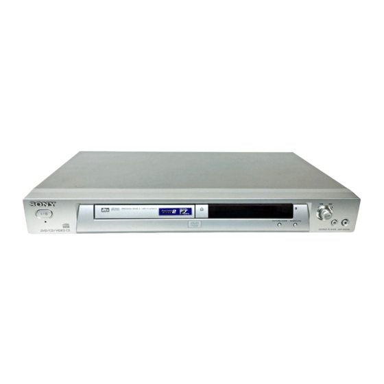
Photo : DVP-NS415
Outputs/Inputs
Outputs
(Jack name: Jack type/Output or Input level/
Load impedance)
LINE IN (AUDIO)*: Phono jack/–/47
kilohms (DVP-NS315/NS415)
LINE OUT (AUDIO): Phono jack/2 Vrms/
Over 10 kilohms
DIGITAL OUT (OPTICAL)*: Optical
output jack/–18 dBm (wave length:
660 nm)
DIGITAL OUT (COAXIAL): Phono jack/
0.5 Vp-p/75 ohms
COMPONENT VIDEO OUT(Y, P
Phono jack/Y: 1.0 Vp-p/P
75 ohms (DVP-NS315/NS415)
LINE IN (VIDEO)*: Phono jack/1.0 Vp-p/
75 ohms
LINE OUT (VIDEO): Phono jack/1.0 Vp-p/
75 ohms
S VIDEO OUT: 4-pin mini DIN/Y:
1.0 Vp-p, C: 0.286 Vp-p/75 ohms
* DVP-NS405/NS410/NS415 only
x
ao
u163
y
i
http://www.xiaoyu163.com
DVP-NS305/NS310/NS315/
NS405/NS410/NS415
2 9
8
RMT-D141A/D142A/D142O/D142P
RMT-D142A
SPECIFICATIONS
(DVP-NS315/NS415)
Q Q
3
6 7
1 3
(DVP-NS305/NS310/NS405/NS410)
, P
):
B
R
, P
: 0.7 Vp-p/
B
R
(DVP-NS315/NS415)
.
9 4
2 8
Canadian Model
DVP-NS305/NS310/NS405/NS410
Hong Kong Model
Saudi Arabia Model
Pakistan Model
Malaysia Model
Middle East Model
Oceania Model
Argentina Model
Brazilian Model
General
1 5
0 5
8
2 9
9 4
Power requirements: 120 V AC, 60 Hz/
110 to 240V AC, 50/60 Hz
See page 1-1 for further information.
Power consumption: 12 W/13 W
See page 1-1 for further information.
Dimensions (approx.): 430 × 62 × 255 mm
(17 × 2
× 10
1
1
in.) (width/height/
/
/
2
8
depth) incl. projecting parts
Mass (approx.): 2.3 kg (5
Operating temperature: 5 ° C to 35 ° C
°
°
(41
F to 95
F)
Operating humidity: 25 % to 80 %
Supplied accessories
See page 1-3.
Specifications and design are subject to
change without notice.
E
S
NERGY
TAR
R
is a U.S. registered mark.
E
S
As an
NERGY
TAR
R
Corporation has determined that this product
E
S
meets the
NERGY
TAR
energy efficiency.
m
CD/DVD PLAYER
co
9 9
US Model
DVP-NS315/NS415
AEP Model
UK Model
DVP-NS305/NS405
Russian Model
Korea Model
Taiwan Model
GA Model
Indian Model
DVP-NS305
DVP-NS305/NS415
PX Model
Mexico Model
Latin Model
DVP-NS315
2 8
9 9
5
/
lb)
64
Partner, Sony
R
guidelines for
Advertisement
Table of Contents

Related Manuals for Sony DVP-NS305


Summary of Contents for Sony DVP-NS305
- Page 1 DVP-NS305/NS310/NS315/ NS405/NS410/NS415 3 7 63 1515 0 RMT-D141A/D142A/D142O/D142P US Model SERVICE MANUAL Canadian Model DVP-NS315/NS415 AEP Model DVP-NS305/NS310/NS405/NS410 UK Model DVP-NS305/NS405 Russian Model Hong Kong Model Korea Model Taiwan Model Saudi Arabia Model GA Model Indian Model Pakistan Model...
- Page 2 DVP-NS305/NS310/NS315/NS405/NS410/NS415 SECTION 3 BLOCK DIAGRAMS 3 7 6 3 1 5 1 5 0 3-1. OVERALL BLOCK DIAGRAM AV-61 BOARD MB-103 BOARD (SEE PAGE 4-31 to 4-34) (SEE PAGE 4-15 to 4-28) IC404 16M SDRAM J103 S VIDEO OUT...
- Page 3 DVP-NS305/NS310/NS315/NS405/NS410/NS415 3 7 6 3 1 5 1 5 0 3-2. RF/SERVO BLOCK DIAGRAM CN202 1 (CD PB) CN202 1 (DVD PB) CN202 3 CN202 3 (CD PLAY) (DVD PLAY) 210mVp-p 20ms/div 640mVp-p 0.2usec/div 440mVp-p 20ms/div 210mVp-p 40usec/div BASE UNIT...
- Page 4 DVP-NS305/NS310/NS315/NS405/NS410/NS415 3 7 6 3 1 5 1 5 0 3-3. SIGNAL PROCESSOR BLOCK DIAGRAM MB-98 BOARD (2/4) (SEE PAGE 4-19 to 4-23) IC404 16M SDRAM IC303 16M DRAM 135-138 140-143 122 124 125 105-108 110-113 145-148 150 127 129 130 IC301 <zzz (CL301)
- Page 5 DVP-NS305/NS310/NS315/NS405/NS410/NS415 3 7 6 3 1 5 1 5 0 3-4. SYSTEM CONTROL BLOCK DIAGRAM MB-103 BOARD (3/4) (SEE PAGE 4-25 to 4-28) IC106 FLASH HA 0 – 21 HA 0 – 21 HD 0 – 15 HD 0 – 15 IC104 tf 1 –...
- Page 6 DVP-NS305/NS310/NS315/NS405/NS410/NS415 3 7 6 3 1 5 1 5 0 3-5. VIDEO BLOCK DIAGRAM AV-61 BOARD (1/2) (SEE PAGE 4-33) IC102 ed J104 (2/2) IC102 VIDEO BUFFER VIDEO 1 2.5Vp-p CN203 (1/2) LINE OUT VIDEO IN VIDEO OUT VIDEO 2 IC102 wl 2.0Vp-p...
- Page 7 DVP-NS305/NS310/NS315/NS405/NS410/NS415 3 7 6 3 1 5 1 5 0 3-6. AUDIO BLOCK DIAGRAM AV-61 BOARD (2/2) (SEE PAGE 4-33) MB-103 BOARD (4/4) (SEE PAGE 4-27) IC204 1 D IN OPTICAL DIGITAL CN601 (3/3) CN203 (2/2) J201 SPDIF Q211...
-
Page 8: Table Of Contents
DVP-NS305/NS310/NS315/NS405/NS410/NS415 3 7 6 3 1 5 1 5 0 3-7. INTERFACE CONTROL BLOCK DIAGRAM IF-89 BOARD (SEE PAGE 4-9) CN404 IC406 REMOTE COMMANDER RECEIVER SYSTEM CONTROL XIFCS XIFCS (SEE PAGE 3-8) XIFBUSY XIFBUSY BUSY XFRRST XFRRST /FRRST CN402... -
Page 9: Dvp-Ns305/Ns310/Ns315/Ns405/Ns410/Ns415 Q Q 3 7 6 3 1 5 1 5
DVP-NS305/NS310/NS315/NS405/NS410/NS415 3 7 6 3 1 5 1 5 0 3-8. POWER BLOCK DIAGRAM (1/2) IF-89 BOARD SWITCHING REGULATOR (SEE PAGE 4-37) (SRV1246JUC) (SEE PAGE 4-37) T101 CN201 CN402 CN401 PS402 D221 L221 POWER EVER+11V AU+11V TRANSFORMER Q404, 405... - Page 10 DVP-NS305/NS310/NS315/NS405/NS410/NS415 3 7 6 3 1 5 1 5 0 3-9. POWER BLOCK DIAGRAM (2/2) AV-61 BOARD (SEE PAGE 4-31 to 4-34) CN202 AI+5V IC103 –5V REG IC102 VIDEO 2 IN BUFFER Q201 AU+11V POWER 1 IC201 (SEE PAGE 3-16)
- Page 11 DVP-NS305/NS310/NS315/NS405/NS410/NS415 SECTION 4 PRINTED WIRING BOARDS AND SCHEMATIC DIAGRAMS 3 7 6 3 1 5 1 5 0 4-1. FRAME SCHEMATIC DIAGRAM J103 S1 VIDEO OUT AUDIO1 AUDIO2 J104 AV-61 BOARD AUDIO1 AUDIO2 LINE OUT VIDEO1 VIDEO2 D1 VIDEO OUT...
- Page 12 DVP-NS305/NS310/NS315/NS405/NS410/NS415 3 7 6 3 1 5 1 5 0 4-2. PRINTED WIRING BOARDS AND SCHEMATIC DIAGRAMS THIS NOTE IS COMMON FOR WIRING BOARDS AND SCHEMATIC DIAGRAMS (In addition to this, the necessary note is printed in each block)
-
Page 13: Http://Www.xiaoyu163.Com
DVP-NS305/NS310/NS315/NS405/NS410/NS415 3 7 6 3 1 5 1 5 0 MB-103 IF-089 AV-61 BOARD BOARD BOARD IC103 8 CN202 3 IC403 tj IC404 3 IC102 ed (CD PLAY) 950mVp-p 4.4Vp-p 37nsec 210mVp-p 2.5Vp-p 20ms/div 3.9Vp-p 125nsec IC103 3 CN202 4... -
Page 14: Xifbusy
DVP-NS305/NS310/NS315/NS405/NS410/NS415 3 7 6 3 1 5 1 5 0 For Schematic Diagram • Refer to page 4-7 for printed wiring board. • Refer to page 4-5 for waveform. IF-89 BOARD IF COM -REF.NO.:3000 SERIES- XX MARK:NO MOUNT B TO B... -
Page 15: Http://Www.xiaoyu163.Com
DVP-NS305/NS310/NS315/NS405/NS410/NS415 3 7 6 3 1 5 1 5 0 For Schematic Diagram • Refer to page 4-11 for printed wiring board. • Refer to page 4-5 for waveforms. MB-103 BOARD(1/7) CN202 DVD/CD RF AMP DIGITAL SERVO -REF.NO.:1000 SERIES-... -
Page 16: Http://Www.xiaoyu163.Com
DVP-NS305/NS310/NS315/NS405/NS410/NS415 3 7 6 3 1 5 1 5 0 For Schematic Diagram • Refer to page 4-11 for printed wiring board. MB-103 BOARD(2/7) SIGNAL PATH MOTOR DRIVE +3.3V SPINDLE SERVO (SPEED AND PHASE) -REF.NO.:1000 SERIES- XX MARK:NO MOUNT... -
Page 17: Xfrrst
DVP-NS305/NS310/NS315/NS405/NS410/NS415 3 7 6 3 1 5 1 5 0 For Schematic Diagram • Refer to page 4-11 for printed wiring board. • Refer to page 4-5 for waveforms. MB-103 BOARD(3/7) SERVO -REF.NO.:1000 SERIES- XX MARK:NO MOUNT NO MARK:PB MODE... -
Page 18: Dvp-Ns305/Ns310/Ns315/Ns405/Ns410/Ns415
DVP-NS305/NS310/NS315/NS405/NS410/NS415 3 7 6 3 1 5 1 5 0 For Schematic Diagram • Refer to page 4-11 for printed wiring board. • Refer to page 4-5 for waveforms. MB-103 BOARD(4/7) AV DECODER -REF.NO.:1000 SERIES- XX MARK:NO MOUNT XWRH... -
Page 19: Http://Www.xiaoyu163.Com
DVP-NS305/NS310/NS315/NS405/NS410/NS415 3 7 6 3 1 5 1 5 0 For Schematic Diagram • Refer to page 4-11 for printed wiring board. MB-103 BOARD(5/7) NO MARK:PB MODE SDRAM -REF.NO.:1000 SERIES- XX MARK:NO MOUNT ADDT0 ADDT0 ADDT15 C437 IC404 MT48LC1M16A1TG-6STR... - Page 20 DVP-NS305/NS310/NS315/NS405/NS410/NS415 3 7 6 3 1 5 1 5 0 For Schematic Diagram • Refer to page 4-11 for printed wiring board. • Refer to page 4-5 for waveform. MB-103 BOARD(6/7) SYSTEM CONTROL -REF.NO.:1000 SERIES- XX MARK:NO MOUNT NO MARK:REC/PB MODE +3.3V...
- Page 21 DVP-NS305/NS310/NS315/NS405/NS410/NS415 3 7 6 3 1 5 1 5 0 For Schematic Diagram • Refer to page 4-11 for printed wiring board. • Refer to page 4-5 for waveforms. R613 R612 MB-103 BOARD(7/7) PR_V COMPOUT R614 FB602 PR_C COUT...
- Page 22 DVP-NS305/NS310/NS315/NS405/NS410/NS415 3 7 6 3 1 5 1 5 0 For Schematic Diagram • Refer to page 4-29 for printed wiring board. AV-61 BOARD(1/2) R201 AUDIO OUT 4700 R210 ± 0.5% 2200 C207 0.01u -REF.NO.:2000 SERIES- C201 R212 560p...
- Page 23 DVP-NS305/NS310/NS315/NS405/NS410/NS415 3 7 6 3 1 5 1 5 0 For Schematic Diagram • Refer to page 4-29 for printed wiring board. • Refer to page 4-6 for waveforms. AV-61 BOARD(2/2) JL117 SW_-13V NOT USE D101 VIDEO OUT D_GND_VIDEO -REF.NO.:2000 SERIES-...
- Page 24 DVP-NS305/NS310/NS315/NS405/NS410/NS415 3 7 6 3 1 5 1 5 0 ER-14 (AV AMP) PRINTED WIRING BOARD • : Uses unleaded solder. 1 3 9 4 2 2 9 6 5 1 3 For printed wiring board Power block There are a few cases that the part printed on AV-61 board this diagram isn’t mounted in this model.
- Page 25 DVP-NS305/NS310/NS315/NS405/NS410/NS415 3 7 6 3 1 5 1 5 0 ER-14 BOARD LINE OUT -REF.NO.: SERIES- IC901 XX MARK:NO MOUNT L905 100uH VIDEO BUFFER CN901 JL933 JL934 R956 JL935 C913 0.22u JL936 IC901 LA73052-TLM C905 JL937 DCCNT1 C907 C903...
- Page 26 DVP-NS305/NS310/NS315/NS405/NS410/NS415 3 7 6 3 1 5 1 5 0 SWITCHING REGULATOR T101 TR010032:HS11S1F TR011019:HS11S1U Q211 POWER TRANSFORMER 2SJ525 L211 HS11S1F D211 R212 D2L20U D313 C211 C213 R211 D213 1SS270A 150u 1.5k Z150 D1NS4/6 ST02D-170 L221 SW201 D221 R313...
-
Page 27: Test Mode
DVP-NS305/NS310/NS315/NS405/NS410/NS415 SECTION 6 3 7 63 1515 0 TEST MODE 6-1. GENERAL DESCRIPTION 6-3. SYSCON DIAGNOSIS The Test Mode allows you to make diagnosis and adjustment eas- The same contents as board detail check by serial interface can be ily using the remote commander and monitor TV. -
Page 28: General Description Of Checking Method
http://www.xiaoyu163.com 3 7 63 1515 0 To quit the diagnosis and return to the Check Menu screen, press General Description of Checking Method x or [ENTER] key. If an error occurred, the diagnosis is suspended 2. Version and the error code is displayed as shown below. (2-2) Revision ROM revision number is displayed. - Page 29 http://www.xiaoyu163.com 3 7 63 1515 0 (3-6) Venc Check (Progressive support model only) (5-4) ARP to RAM Address Bus Data write t read, and accord check Data write t other address read discord check Error: 52: Write/read data discord Error 10: ARP Tt RAM address bus error Error may occur due to defect of access with syscon.
- Page 30 http://www.xiaoyu163.com 3 7 63 1515 0 6. AV Decoder 8. Audio Output (8-2) ARP t1935 (6-2) 1935 RAM Data flow from supply system DRAM to SDRAM of AV Data write t read, and accord check Decoder is tested. Error 13: AVD RAM read data discord Error 14: ARP t 1935 video NG The program code data stored in ROM (IC107) are copied 15: ARP t 1935 audio NG...
- Page 31 http://www.xiaoyu163.com 3 7 63 1515 0 Error Codes List 6-4. DRIVE AUTO ADJUSTMENT 00: Error not detected On the Test Mode Menu screen, press [1] key on the remote com- 01: RAM write/read data discord mander, and the drive auto adjustment menu will be displayed. 02: Gate array NG 03: EEPROM NG ## Drive Auto Adjustment ##...
- Page 32 http://www.xiaoyu163.com 3 7 63 1515 0 1. DVD Single Layer Disc 3. DVD Dual Layer Disc Select [1], insert DVD single layer disc, and press [ENTER] key, Select [3], insert DVD dual layer disc, and press [ENTER] key, and and the adjustment will be made through the following steps, then the adjustment will be made through the following steps, then ad- adjusted values will be written to the EEPROM.
- Page 33 http://www.xiaoyu163.com 3 7 63 1515 0 0. Disc Check Memory 6-5. DRIVE MANUAL OPERATION On the Test Mode Menu screen, select [2], and the manual opera- Disc Check tion menu will be displayed. For the manual operation, each servo on/off control and adjustment can be executed manually. 1.
- Page 34 http://www.xiaoyu163.com 3 7 63 1515 0 2. Servo Control Once the disc type has been selected, the sector address or time code display field will appear as shown below. These values are displayed when PLL is locked. Servo Control 1. LD R.
- Page 35 http://www.xiaoyu163.com 3 7 63 1515 0 3. Track/Layer Jump 4. Manual Adjustment Track/Layer Jump Manual Adjustment:Up/Down 1. 1Tj FWD R. Fj (L1->L0) 1. TRK. Offset 2. 1Tj REV L. Fj (L0->L1) 2. Focus Gain 3. 2Tj FWD U. Lj (L1->L0) 3.
- Page 36 http://www.xiaoyu163.com 3 7 63 1515 0 5. Auto Adjustment 6. Memory Check The display image is shown below and three screens in total can be selected. Auto Adjustment 1. Auto TRK. Offset DL 2. Auto Focus Balance EEPROM DATA 1 3.
- Page 37 http://www.xiaoyu163.com 3 7 63 1515 0 6-6. MECHA AGING 6-8. VERSION INFORMATION ### Version Infomation ### ### Mecha Aging ### IF con. Ver.x.xxx(xxxx) Group SYScon. Ver.x.xxx(xxxx) Press OPEN key Model Region 0x Servo DSP Ver:x.xxx AVD ucode Ver:xxxxxxxx Abort : STOP key OPT TYPE : x LASER Exit : RETURN On the Test Mode Menu screen, selecting [3] executes the aging...
- Page 38 http://www.xiaoyu163.com 3 7 63 1515 0 2. OPERATION OF SELF CHECK MODE 6-10. IF CON SELF DIAGNOSTIC FUNCTION The Self Check mode is the function to conduct the basic test to the FL display and DVD panel section. 1. IF-89 BOARD (IF CON) TEST MODE The IF-89 board (IF CON) test mode is the IF CON self-diagnosis 2-1.
- Page 39 http://www.xiaoyu163.com 3 7 63 1515 0 2-2. Operation of Auto Self Check When the Self Check mode becomes active at the AC Power ON or by key input, the test display of the following steps (1) to (4) is repeated. (1) FLD and LED all ON (for 5 seconds) (2) MODEL display (for 2 seconds) (3) Version display (for 2 seconds)
- Page 40 http://www.xiaoyu163.com 3 7 63 1515 0 2-3. Each Self Check Function Each Self Check function tests the FLD display, LED display, and key input. IC404: Pin No. (Signal) Input Voltage [V] (BNRKEY) (PLAY) (O/C) (TVS) Pin ed Pin ef Pin eg Pin eh 0 –...
- Page 41 http://www.xiaoyu163.com 3 7 63 1515 0 • Key code display (at input of H key, key code: 0 Ah) • At input of faulty voltage • When key is pressed double 2-3-3. Remote Commander Key Name Display and Key Code Display 2-3-3-1.
- Page 42 http://www.xiaoyu163.com 3 7 63 1515 0 2-3-4. Communication Monitoring Display The communication state is monitored and displayed while the key name on the main unit and the remote commander is displayed. When the communication to the System Controller failed, VIDEO CD, DVD, and CD segments turn on.
-
Page 43: Play
http://www.xiaoyu163.com 3 7 63 1515 0 2-3-6. FLD Grid Test Display and SHUTTLE Click Opera- tion Test 2-3-6-1. Transition Keys in Self Check Mode • key on the remote commander • SHUTTLE on the remote commander during Grid Test display (This unit does not provide JOG/SHUTTLE, and therefore use an- other DVD remote commander having the JOG/SHUTTLE) 2-3-6-2. - Page 44 http://www.xiaoyu163.com 3 7 63 1515 0 L 13942296513 ( 7G-1G) ANODE CONNECTION u163 6-18 http://www.xiaoyu163.com...
- Page 45 http://www.xiaoyu163.com 3 7 63 1515 0 1-3. Clock signal check 6-11. TROUBLESHOOTING Measure the clock signal frequency at CPUCK (CL101) of 6-11-1. Cannot Enter Test Mode SYSCON (IC104) with an oscilloscope. You cannot enter the Test mode when either button has been pressed If the 8.25 MHz signal appears.
- Page 46 http://www.xiaoyu163.com 3 7 63 1515 0 1-3-2. When the 33 MHz signal appears at CPUCK 3. If the message “SDSP No Ack” appears after the menu • WAIT signal check is displayed. Observe XWAIT (pin-yj) of SYSCON (IC104) with an os- 3-1.
- Page 47 http://www.xiaoyu163.com 3 7 63 1515 0 6-11-4. The product itself is defective. 3-3. Check IFBSY (pin-5), XIFCS (pin-6), SI0 (pin-4), • If MB103 does not have any problem, SO0 (pin-1) and SC0 (pin-3) at CN101 The board other than MB-103 board is defective or connec- If they are fixed to “H”...