
Related Manuals for National Instruments DAQ PCI-4451


Summary of Contents for National Instruments DAQ PCI-4451
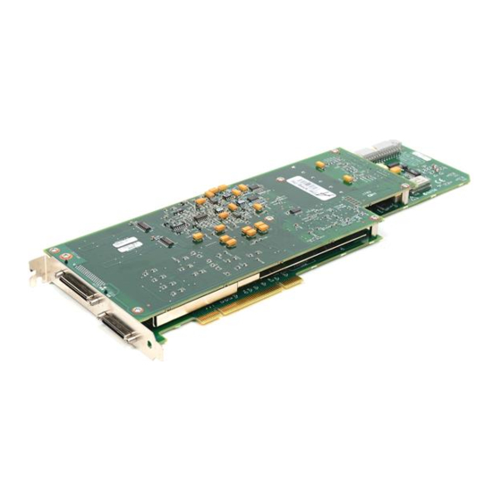
- Page 1 PCI-4451/4452 User Manual Dynamic Signal Acquisition Device for PCI April 1998 Edition Part Number 321891A-01...
- Page 2 Singapore 2265886, Spain 91 640 0085, Sweden 08 730 49 70, Switzerland 056 200 51 51, Taiwan 02 377 1200, United Kingdom 01635 523545 National Instruments Corporate Headquarters 6504 Bridge Point Parkway Austin, Texas 78730-5039 USA Tel: 512 794 0100 © Copyright 1998 National Instruments Corporation. All rights reserved.
-
Page 3: Important Information
Important Information Warranty The PCI-4451/4452 is warranted against defects in materials and workmanship for a period of one year from the date of shipment, as evidenced by receipts or other documentation. National Instruments will, at its option, repair or replace equipment that proves to be defective during the warranty period. -
Page 4: Table Of Contents
Customer Communication ...xi Chapter 1 Introduction What You Need to Get Started ...1-2 Unpacking ...1-2 Software Programming Choices ...1-3 National Instruments Application Software ...1-3 Optional Equipment ...1-4 Custom Cabling ...1-4 Chapter 2 Installation and Configuration Software Installation ...2-1 Hardware Installation...2-1 Device Configuration...2-2... - Page 5 GPCTR0_GATE Signal ... 4-20 GPCTR0_OUT Signal ... 4-20 GPCTR0_UP_DOWN Signal... 4-20 GPCTR1_SOURCE Signal ... 4-21 GPCTR1_GATE Signal ... 4-21 GPCTR1_OUT Signal ... 4-22 GPCTR1_UP_DOWN Signal... 4-22 FREQ_OUT Signal... 4-24 Field Wiring Considerations... 4-24 PCI-4451/4452 User Manual © National Instruments Corporation...
- Page 6 Antialias Filtering...6-3 The ADC ...6-8 Noise...6-9 Analog Output Circuitry ...6-10 Anti-Image Filtering...6-10 The DAC ...6-12 Calibration ...6-12 Mute Feature...6-13 Appendix A Specifications Appendix B Pin Connections Appendix C Customer Communication Glossary Index © National Instruments Corporation PCI-4451/4452 User Manual Contents...
- Page 7 Table 4-1. Analog I/O Connector Pin Assignment ... 4-3 Table 4-2. Analog I/O Signal Summary... 4-4 Table 4-3. Digital I/O Connector Pin Assignment ... 4-6 Table 4-4. Digital I/O Signal Summary ... 4-8 PCI-4451/4452 User Manual viii © National Instruments Corporation...
-
Page 8: About This Manual
PCI-4451/4452 device. Chapter 4, Signal Connections, describes how to make input and output connections to your PCI-4451/4452 device via the analog I/O and digital I/O connectors of the device. Chapter 5, Calibration, discusses the calibration procedures for your PCI-4451/4452 device. -
Page 9: Conventions Used In This Manual
This font also denotes text from which you supply the appropriate word or value, as in NI-DAQ 6.x. SE means referenced single ended (RSE). SE and RSE are equivilant. PCI-4451/4452 User Manual Glossary contains an alphabetical list and description of terms used in this manual, including abbreviations, acronyms, metric prefixes, mnemonics, and symbols. -
Page 10: National Instruments Documentation
National Instruments Documentation The PCI-4451/4452 User Manual is one piece of the documentation set for your DAQ system. You could have any of several types of manuals depending on the hardware and software in your system. Use the manuals you have as follows: •... -
Page 11: Introduction
51.2 kS/s, while the PCI-4452 has four channels of 16-bit simultaneously sampled analog input at 204.8 kS/s. Information on analog output applies only to the PCI-4451, where as information on analog input applies to both the PCI-4451 and the PCI-4452. -
Page 12: What You Need To Get Started
Chapter 1 Introduction What You Need to Get Started To set up and use your PCI-4451 or PCI-4452, you will need the following: Unpacking Your PCI-4451/4452 is shipped in an antistatic plastic package to prevent electrostatic damage to the device. Electrostatic discharge can damage components on the instrument. -
Page 13: Software Programming Choices
Software Programming Choices There are several options to choose from to program and use your National Instruments device. You can use LabVIEW for Windows, LabWindows/CVI for Windows, VirtualBench-DSA, ComponentWorks, and Measure. National Instruments Application Software LabVIEW and LabWindows/CVI are innovative program development software packages for data acquisition and control applications. -
Page 14: Optional Equipment
Custom Cabling National Instruments offers cables of different lengths and the BNC-2140 DSA accessory to connect your analog I/O to the PCI-4451/4452. National Instruments recommends you do not develop your own cabling solution due to the difficulty of working with the high-density connector and the need to maintain high signal integrity. - Page 15 • National Instruments also offers cables of different lengths and accessories to connect your digital I/O signals to the PCI-4451/4452. To develop your own cable, the mating connector for the digital I/O is a 50-position receptacle. For a connector pinout assignment, refer to Table 4-3,...
-
Page 16: Installation And Configuration
Remove the top cover or access port to the I/O channel. Remove the expansion slot cover on the back panel of the computer. Insert the PCI-4451/4452 device into a 5 V PCI slot. It should fit snugly, but do not force the device into place. -
Page 17: Device Configuration
Chapter 2 Installation and Configuration The PCI-4451/4452 device is now installed. You are now ready to configure your software. Device Configuration The PCI-4451/4452 devices are completely software configurable. However, you must perform two types of configuration—bus-related and data acquisition-related. The PCI-4451/4452 devices are fully compatible with the industry standard PCI Local Bus Specification Revision 2.0. -
Page 18: Hardware Overview
Hardware Overview This chapter presents an overview of the hardware functions on your PCI-4451/4452 device. Figure 3-1 shows a block diagram of the digital functions. Figure 3-2 shows a block diagram of the analog functions. The two function blocks connect through the analog mezzanine bus. -
Page 19: Figure 3-2. Analog Function Block Diagram
Chapter 3 Hardware Overview Figure 3-2. Analog Function Block Diagram PCI-4451/4452 User Manual © National Instruments Corporation... -
Page 20: Analog Input
The PCI-4451/4452 devices operate in bipolar mode. Bipolar input means that the input voltage range is between –V The PCI-4451/4452 has a bipolar input range of 20 V (±10 V) for a gain of 1.0 (0 dB). You can program the range settings on a per channel basis so that you can configure each input channel uniquely. -
Page 21: Considerations For Selecting Input Ranges
If the input range is not appropriately chosen, an input signal can be clipped and introduce large errors that are easily identified in the frequency spectrum. The PCI-4451/4452 is equipped with overrange detection circuits in both the analog and digital sections of each input channel. These circuits determine if an input signal has exceeded the selected input voltage. -
Page 22: Analog Output
You can select different analog output configurations through application software designed to control the PCI-4451. The following sections describe in detail each of the analog output categories. The PCI-4451 device has two channels of analog output voltage at the I/O connector. -
Page 23: Trigger
Trigger In addition to supporting internal software triggering and external digital triggering to initiate a data acquisition sequence, the PCI-4451/4452 also supports analog level triggering. You can configure the trigger circuit to monitor any one of the analog input channels to generate the level trigger. -
Page 24: Figure 3-3. Below-Low-Level Triggering Mode
In below-low-level triggering mode, shown in Figure 3-3, the trigger is generated when the signal value is less than lowValue. HighValue is unused. lowValue Trigger Figure 3-3. Below-Low-Level Triggering Mode © National Instruments Corporation PCI-4451/4452 User Manual... -
Page 25: Figure 3-4. Above-High-Level Triggering Mode
In high-hysteresis triggering mode, the trigger is generated when the signal value is greater than highValue, with the hysteresis specified by lowValue. PCI-4451/4452 User Manual highValue Trigger Figure 3-4. Above-High-Level Triggering Mode... -
Page 26: Rtsi Triggers
You can trigger the PCI-DSA devices from any other PCI-DSA device or any National Instruments device that has the RTSI bus feature. You can connect the devices through the RTSI bus cable. An external digital trigger can also trigger multiple devices simultaneously by distributing that trigger through the RTSI bus. -
Page 27: Digital I/O
Refer to the Chapter 4, shown in Figure 3-8. Digital I/O The PCI-4451/4452 devices contain eight lines of digital I/O for general-purpose use through the 50-pin connector. You can individually software-configure each line for either input or output. The hardware up/down control for general-purpose counters 0 and 1 are connected onboard to DIO6 and DIO7, respectively. -
Page 28: Timing Signal Routing
Timing Signal Routing The DAQ-STC provides a flexible interface for connecting timing signals to other devices or to external circuitry. Your PCI-4451/4452 device uses the RTSI bus to interconnect timing signals between devices, and uses the PFI pins on the I/O connector to connect the device to external circuitry. -
Page 29: Selecting Sample/Update Clock Frequency
Selecting Sample/Update Clock Frequency The two analog input channels of the PCI-4451 and the four inputs of the PCI-4452 are simultaneously sampled at any software-programmable rate from 5.0 kS/s to 204.8 kS/s in 190.7 S/s increments (worst case). The devices use direct digital synthesis (DDS) technology so that you can choose the correct sample rate required for your application. -
Page 30: Device Configuration Issues
1.25 kS/s. This minimum rate is required to keep the internal circuitry of the converters running within specifications. You are responsible for selecting sample and update rates that fall within the specified limits. Failure to do so could greatly affect the specifications. © National Instruments Corporation Chapter 3 Theory of Analog 3-13 Hardware Overview Operation. -
Page 31: Signal Connections
BNC-2140. You can connect the analog I/O signals to the shielded cable through a single 68-pin connector. The digital I/O connector for the PCI-4451/4452 has 50 pins that you can connect to generic 68-pin terminal blocks through the SHC50-68 shielded cable. -
Page 32: Analog I/O Connector Signal Descriptions
Chapter 4 Signal Connections Analog I/O Connector Signal Descriptions Figure 4-1 shows the analog pin connections for the PCI-4451/4452. PCI-4451/4452 User Manual -ACH0 +ACH0 -ACH1 +ACH1 ACH2- +ACH2 -ACH3 +ACH3 10 44 11 45 12 46 13 47 14 48... -
Page 33: Table 4-1. Analog I/O Connector Pin Assignment
Analog Output Ground—The analog output voltages are ultimately referenced to this node. All three ground references—AIGND, AOGND, and DGND—are connected together on your PCI-4451/4452 device, but each serves a separate purpose. Output +5 VDC Source—These pins are fused for up to 0.5 A and supply power to the DSA signal conditioning accessories. -
Page 34: Table 4-2. Analog I/O Signal Summary
DIO = Digital Input/Output AO = Analog Output DO = Digital Output † ±400 V/±400 V guaranteed by design, but not tested or certified to operate beyond ±42.4 V PCI-4451/4452 User Manual Table 4-2. Analog I/O Signal Summary Impedance Protection Input/... -
Page 35: Digital I/O Connector Signal Descriptions
Digital I/O Connector Signal Descriptions Figure 4-2 shows the digital pin connections for the PCI-4451/4452. Refer to Appendix B, the 68-pin connector. © National Instruments Corporation FREQ_OUT GPCTR0_OUT PFI8/GPCTR0_SOURCE PFI6/WFTRIG PFI7 GPCTR1_OUT PFI3/GPCTR1_SOURCE PFI1/TRIG2 (PRETRIG) CONVERT* 10 35 DIO(7) 11 36... -
Page 36: Table 4-3. Digital I/O Connector Pin Assignment
CONVERT* DGND PFI3/GPCTR1_SOURCE DGND PFI4/GPCTR1_GATE DGND UPDATE* DGND PCI-4451/4452 User Manual Direction Input or Digital I/O channels 0 through 7—Channels 6 and 7 can Output control the up/down signal of general-purpose counters 0 and 1, respectively. — Digital Ground—This pin supplies the reference for the digital signals at the I/O connector as well as the +5 VDC supply. - Page 37 DGND PFI9/GPCTR0_GATE DGND GPCTR0_OUT DGND FREQ_OUT DGND © National Instruments Corporation Direction Output General-Purpose Counter 1 Output Input PFI6/Waveform Trigger—As an input, this is one of the PFIs. Output As an output, this is the WFTRIG signal. In timed analog output sequences, a low-to-high transition indicates the initiation of the waveform generation.
-
Page 38: Table 4-4. Digital I/O Signal Summary
DIO = Digital Input/Output DO = Digital Output Note: The tolerance on the 50 k pullup and pulldown resistors is very large. Actual value may range between 17 and 100 k . PCI-4451/4452 User Manual Table 4-4. Digital I/O Signal Summary Impedance... -
Page 39: Analog Input Signal Connections
AIGND is an analog input common signal that connects directly to the ground system on the PCI-4451/4452 devices. You can use this signal for a general analog ground tie point to your PCI-4451/4452 device if necessary, but connecting AIGND to other earth-connected grounds is not recommended. -
Page 40: Types Of Signal Sources
A ground-referenced signal source connects in some way to the building system ground and is, therefore, already connected to a common ground point with respect to the PCI-4451/4452 device, assuming that you plug the computer into the same power system. Nonisolated outputs of instruments and devices that plug into the building power system fall into this category. -
Page 41: Analog Output Signal Connections
AOGND is a ground-reference signal for both analog output channels. It is connected directly to the ground system on the PCI-4451 device. You can use this signal for a general analog ground tie point to your PCI-4451 device if necessary, but connecting AOGND to other earth-connected grounds is not recommended. -
Page 42: Analog Power Connections
Caution ground, digital ground, or to any other voltage source on the PCI-4451/4452 device or any other device. Doing so can damage the PCI-4451/4452 device and the computer. National Instruments is not liable for damages resulting from such a connection. -
Page 43: Figure 4-5. Digital I/O Connections
Digital input applications include receiving TTL signals and sensing external device states such as the state of the switch shown in Figure 4-5. Digital output applications include sending TTL signals and driving external devices such as the LED shown in Figure 4-5. -
Page 44: Digital Power Connections
Do not under any circumstances connect these +5 V power pins directly to analog ground, digital ground, or to any other voltage source on the PCI-4451/4452 device or any other device. Doing so can damage the PCI-4451/4452 device and the computer. National Instruments is not liable for damages resulting from such a connection. -
Page 45: Acquisition Timing Connections
Posttriggered data acquisition allows you to view only data that is acquired after a trigger event is received. A typical posttriggered acquisition sequence is shown in Figure 4-6. Scan Counter © National Instruments Corporation TRIG1 CONVERT* Figure 4-6. Typical Posttriggered Acquisition... -
Page 46: Pfi0/Trig1 (Ext_Trig) Signal
The selected edge of the PFI0/TRIG1 signal starts the data acquisition sequence for both posttriggered and pretriggered acquisitions. The PCI-4451/4452 supports analog level triggering on the PFI0/TRIG1 pin. See Chapter 3,... -
Page 47: Pfi1/Trig2 (Pretrig) Signal
The CONVERT* signal reflects the end of delta-sigma conversion on the ADC. The output is an active-low pulse with a pulse width of 70 to 100 ns. This output is set to tri-state at startup. © National Instruments Corporation 4-17 PCI-4451/4452 User Manual... -
Page 48: Extstrobe* Signal
The UPDATE* signal reflects the end of a delta-sigma conversion on the DACs. The output is an active-low pulse with a pulse width of 70 to 100 ns. This output is set to tri-state at startup. PCI-4451/4452 User Manual = 600 ns or 5 s Figure 4-8. EXTSTROBE* Signal Timing 4-18 ©... -
Page 49: General-Purpose Timing Signal Connections
23 ns high or low. There is no minimum frequency limitation. The 20 MHz or 100 kHz timebase normally generates the GPCTR0_SOURCE signal unless you select some external source. © National Instruments Corporation = 50 ns minimum = 23 ns minimum Figure 4-9. -
Page 50: Gpctr0_Gate Signal
You can disable this input so that software can control the up-down functionality and leave the DIO6 pin free for general use. PCI-4451/4452 User Manual Figure 4-10. GPCTR0_OUT Signal Timing 4-20... -
Page 51: Gpctr1_Source Signal
You can use the gate signal in a variety of different applications to perform such actions as starting and stopping the counter, generating interrupts, saving the counter contents, and so on. © National Instruments Corporation 4-21 PCI-4451/4452 User Manual... -
Page 52: Figure 4-12. Gpctr1_Out Signal Timing
DIO7 pin free for general use. Figure 4-13 shows the timing requirements for the GATE and SOURCE input signals and the timing specifications for the OUT output signals of your PCI-4451/4452 device. PCI-4451/4452 User Manual Figure 4-12. GPCTR1_OUT Signal Timing 4-22 ©... -
Page 53: Figure 4-13. Gpctr Timing Summary
The GATE input timing parameters are referenced to the signal at the SOURCE input or to one of the internally generated signals on your PCI-4451/4452 device. Figure 4-13 shows the GATE signal referenced to the rising edge of a source signal. The gate must be valid (either high or... -
Page 54: Freq_Out Signal
Field Wiring Considerations Environmental noise can seriously influence the accuracy of measurements made with your PCI-4451/4452 device if you do not take proper care when running signal wires between signal sources and the device. The following recommendations apply mainly to analog input signal routing to the device, although they also apply to signal routing in general. - Page 55 Separate PCI-4451/4452 device signal lines from high-current or high-voltage lines. These lines can induce currents in or voltages on the PCI-4451/4452 device signal lines if they run in parallel paths at a close distance. To reduce the magnetic coupling between lines, separate them by a reasonable distance if they run in parallel, or run the lines at right angles to each other.
-
Page 56: Loading Calibration Constants
Calibration This chapter discusses the calibration procedures for your PCI-4451/4452 device. Your PCI-4451/4452 is shipped with a calibration certificate. The traceability information is stored in National Instruments corporate databases and is not actually shown on your certificate. The certificate contains a unique tracking number linking your device to the database. You can get a detailed calibration report from National Instruments for an additional charge. -
Page 57: Self-Calibration
It is better to self-calibrate when you install the device in your environment. Self-Calibration Your PCI-4451/4452 device can measure and correct for almost all of its calibration-related errors without any external signal connections. Your National Instruments software provides a self-calibration method. This self-calibration process, which generally takes less than a minute, is the preferred method of assuring accuracy in your application. -
Page 58: Traceable Recalibration
If you require factory recalibration, send your PCI-4451/4452 back to National Instruments. The device will be sent back to you with a new calibration certificate. A detailed report may be requested for an additional fee. Please check with National Instruments for additional information such as cost and delivery times. -
Page 59: Theory Of Analog Operation
See Figure 3-2, diagram of the PCI-4451/4452 analog functions. Analog Input Circuitry The PCI-4451 has two identical analog input channels. The PCI-4452 has four identical analog input channels. An analog input channel is illustrated in Figure 4-3, These input channels have 16-bit resolution and are simultaneously sampled at software-programmable rates from 5 to 204.8 kS/s in 190.7 µS/s... -
Page 60: Input Coupling
Chapter 6 Theory of Analog Operation The 90 dB dynamic range of the PCI-4451/4452 devices is the result of low noise and distortion and makes possible high-accuracy measurements. The devices have excellent amplitude flatness of ±0.1 dB, and have a maximum total harmonic distortion (THD) specification of 92 dB at 1 kHz and a worst case THD of 80 dB at higher frequencies. -
Page 61: Antialias Filtering
The PCI-4451/4452 has complete antialiasing filters. The PCI-4451/4452 includes two stages of antialias filtering in each input channel lowpass filter. This filter has a cutoff frequency of about 4 MHz and a rejection of greater than 40 dB at 20 MHz. - Page 62 128 times the sample rate. The analog filter in each channel rejects possible aliases (mostly noise) from signals that lie near these multiples. Figures 6-1 and 6-2 show the frequency response of the PCI-4451/4452 input circuitry. PCI-4451/4452 User Manual...
-
Page 63: Figure 6-1. Input Frequency Response
Amplitude (dB) 0.00 –20.00 –40.00 –60.00 –80.00 –100.00 –120.00 0.00 0.20 © National Instruments Corporation Chapter 6 0.40 0.60 Frequency/Sample Rate (f Figure 6-1. Input Frequency Response Theory of Analog Operation 0.80 1.00 PCI-4451/4452 User Manual... -
Page 64: Figure 6-2. Input Frequency Response Near The Cutoff
This means that, although the filter has good alias rejection for high sample rates, it does not reject as well at lower sample rates. The alias rejection near 128 times the sample rate PCI-4451/4452 User Manual 0.45 0.46 0.47... -
Page 65: Figure 6-3. Alias Rejection At The Oversample Rate
48 kS/s. The signal-to-THD plus noise ratio is 35 dB for the clipped waveform and 92 dB for the properly ranged waveform. Notice that aliases of all the harmonics due to clipping appear in Figure 6-4. © National Instruments Corporation Chapter 6 10 kS/s 100 kS/s 12.8 MHz... -
Page 66: The Adc
The ADC The PCI-4451/4452 ADCs use a method of A/D conversion known as delta-sigma modulation. If the data rate is 204.8 kS/s, each ADC actually samples its input signal at 26.2144 MS/s (128 times the data rate) and produces 1-bit samples that are applied to the digital filter. -
Page 67: Noise
32,768/1.414 = 23,170.475 least significant bits (LSBs). A grounded channel of the PCI-4451/4452 has a noise level of about 0.65 LSB rms (this amount fluctuates). The ratio of 23,170.475 / 0.65 is about 35647, or 91.0 dB—the dynamic range. Several factors can degrade the noise performance of the inputs. -
Page 68: Analog Output Circuitry
Because the sample data actually represents only the frequency components below one-half the sample rate (the baseband), it is desirable to filter out all these extra images of the signal. The PCI-4451 accomplishes this filtering in two stages. First, the data is digitally resampled at eight times the original sample rate. -
Page 69: Figure 6-5. Signal Spectra In The Dac
Figure 6-5c. Still, images remain and they must be filtered out. Each output channel of the PCI-4451 has discrete-time (switched-capacitor) and continuous-time analog filters that remove the high-frequency images, as shown in Figure 6-5d. - Page 70 Theory of Analog Operation The DAC The 64-times oversampling delta-sigma DACs on the PCI-4451 work in the same way as delta-sigma ADCs, only in reverse. The digital data first passes through a digital lowpass filter and then goes to the delta-sigma modulator.
-
Page 71: Mute Feature
Mute Feature The two-channel DAC chip on the PCI-4451 goes into mute mode if the chip receives at least 4,096 consecutive zero values on both channels at once. In mute mode, the outputs clamp to ground and the noise floor drops from about 92 dB below full-scale to about 120 dB below full-scale. -
Page 72: Specifications
Specifications This appendix lists the specifications of the PCI-4451/4452. These specifications are typical at 25° C unless otherwise noted. The system must be allowed to warm-up for 15 minutes to achieve the rated accuracy. Note Be sure to keep the cover on your computer to maintain forced air cooling. - Page 73 FIFO buffer size...512 samples Data transfers ...DMA, programmed I/O, interrupt Transfer Characteristics INL (relative accuracy)...±2 LSB DNL ...±0.5 LSB typ, ±1 LSB max, Offset (residual DC) Gain (amplitude accuracy)...±0.1 dB, f PCI-4451/4452 User Manual Gain Linear 31.6 +30 dB +40 dB +50 dB...
- Page 74 Common-mode range Overvoltage protection... ±42.4 V, powered on or off Common mode rejection ratio © National Instruments Corporation Gain 0, +10, +20, +30, +40 dB... ±0.1 dB, 0 to 95 kHz, 204.8 kS/s, 20, 10, +50, +60 dB ... ±1 dB, 0 to 95 kHz, ±0.1 dB, AC 3 dB cutoff frequency ...
-
Page 75: Figure A-1. Idle Channel Noise (Typical)
Input noise spectral density ...8 nV/ Dynamic Characteristics Alias-free bandwidth ...DC to 0.464 f Alias rejection...80 dB, 0.536 f Spurious-free dynamic range...95 dB Crosstalk (channel separation) PCI-4451/4452 User Manual 10,000 100,000 Sample Rate (S/s) Figure A-1. Idle Channel Noise (Typical) Gain = +60 dB... - Page 76 Resolution ... 16 bits Type of DAC... Delta-sigma, 64-times Sample rates ... 1.25 to 51.2 kS/s in increments Frequency accuracy... ±100 ppm © National Instruments Corporation Appendix A ±2°, Gain < 0 dB ±2°, Gain < 0 dB (same configuration all input...
-
Page 77: Idle Channel Noise (Typical
Frequency response ...±0.2 dB, 0 to 23 kHz, 51.2 kS/s 3 dB bandwidth...0.492 f Output coupling ...DC Short-circuit protection...yes (+ and may be shorted Outputs protected...±DAC0OUT, ±DAC1OUT Idle channel noise PCI-4451/4452 User Manual Attenuation Linear 0 dB 20 dB 40 dB... -
Page 78: Dynamic Characteristics
Signal delay... 34.6 ±0.5 sample periods, any Digital I/O Number of channels ... 8 input/output Compatibility ... TTL/CMOS © National Instruments Corporation Appendix A 80 dB; 90 dB for f or signal < 1 V 90 dB (CCIF 14 kHz + 15 kHz) - Page 79 Base clock accuracy...±0.01% Max source frequency...20 MHz Min source pulse duration ...10 ns, edge-detect mode Min gate pulse duration ...10 ns, edge-detect mode Data transfers ...DMA, interrupts, PCI-4451/4452 User Manual Level = 0 V) = 5 V) = 24 mA) = 13 mA) Counter/timers ...24 bits...
-
Page 80: Analog Trigger
Pulse width ... 10 ns min Bus Interface Type ... PCI Master/Slave Power Requirement Power (PCI-4451) ... +5 V, 1.7 A idle, 2.0 A active Power (PCI-4452) ... +5 V, 2.2 A idle, 2.5 A active © National Instruments Corporation PCI-4451 ... ACH<0..1>... - Page 81 Operating temperature ...0° C to +40° C Storage temperature range Relative humidity ...10% to 95%, no condensation Calibration Calibration interval ...1 year PCI-4451/4452 User Manual (4.19 by 12.28 by 0.73 in.) 25° C to +85° C A-10 © National Instruments Corporation...
- Page 82 Pin Connections This appendix describes the pin connections on the optional 68-pin digital accessories for the PCI-4451 and PCI-4452 devices. © National Instruments Corporation PCI-4451/4452 User Manual...
-
Page 83: Figure B-1. 68-Pin Digital Connector For Any Digital Accessory
Appendix B Pin Connections PCI-4451/4452 User Manual FREQ_OUT PFI9/GPCTR0_GATE GPCTR0_OUT PFI8/GPCTR0_SOURCE UPDATE* PFI6/WFTRIG PFI7 PFI4/GPCTR1_GATE GPCTR1_OUT PFI3/GPCTR1_SOURCE PFI0/TRIG1 (EXT_TRIG) PFI1/TRIG2 (PRETRIG) CONVERT* RESERVED1 DIO(7) DIO(6) DIO(5) DIO(4) DIO(3) EXTSTROBE* DIO(2) DIO(1) DIO(0) +5 V Figure B-1. 68-Pin Digital Connector for any Digital Accessory... -
Page 84: Electronic Services
Electronic Services Bulletin Board Support National Instruments has BBS and FTP sites dedicated for 24-hour support with a collection of files and documents to answer most common customer questions. From these sites, you can also download the latest instrument drivers, updates, and example programs. For recorded instructions on how to use the bulletin board and FTP services and for BBS automated information, call 512 795 6990. - Page 85 Telephone and Fax Support National Instruments has branch offices all over the world. Use the list below to find the technical support number for your country. If there is no National Instruments office in your country, contact the source from which you purchased your software to obtain support.
- Page 86 National Instruments for technical support helps our applications engineers answer your questions more efficiently. If you are using any National Instruments hardware or software products related to this problem, include the configuration forms from their user manuals. Include additional pages if necessary.
- Page 87 Complete a new copy of this form each time you revise your software or hardware configuration, and use this form as a reference for your current configuration. Completing this form accurately before contacting National Instruments for technical support helps our applications engineers answer your questions more efficiently.
- Page 88 Documentation Comment Form National Instruments encourages you to comment on the documentation supplied with our products. This information helps us provide quality products to meet your needs. Title: PCI-4451/4452 User Manual Edition Date: April 1998 Part Number: 321891A-01 Please comment on the completeness, clarity, and organization of the manual.
- Page 89 – negative of, or minus amperes alternating current AC coupled allowing the transmission of AC signals while blocking DC signals analog-to-digital © National Instruments Corporation Value –12 –9 – 6 –3 PCI-4451/4452 User Manual...
- Page 90 PCI-4451/4452 User Manual © National Instruments Corporation...
- Page 91 Analog signals can be single-ended or differential. For digital signals, you group channels to form ports. Ports usually consist of either four or eight digital channels. circuit trigger a condition for starting or stopping clocks © National Instruments Corporation PCI-4451/4452 User Manual Glossary...
- Page 92 (timing) coupling the manner in which a signal is connected from one location to another crosstalk an unwanted signal on one channel due to an input on a different channel PCI-4451/4452 User Manual © National Instruments Corporation...
- Page 93 If you do change the value of such a parameter, the new value becomes the new setting. You can set default settings for some parameters in the configuration utility or manually using switches located on the device. © National Instruments Corporation ), for signals in volts PCI-4451/4452 User Manual Glossary...
- Page 94 GPIB interface board dynamic range the ratio of the largest signal level a circuit can handle to the smallest signal level it can handle (usually taken to be the noise level), normally expressed in decibels PCI-4451/4452 User Manual © National Instruments Corporation...
- Page 95 FIFO ahead of time. This again reduces the effect of latencies associated with getting the data from system memory to the DAQ device. © National Instruments Corporation PCI-4451/4452 User Manual Glossary...
- Page 96 0 clock source signal GPCTR1_GATE general-purpose counter timer 1 gate signal GPCTR1_OUT general-purpose counter timer 1 output signal GPCTR1_SOURCE general-purpose counter timer 1 clock source signal grounded measurement See SE. system PCI-4451/4452 User Manual © National Instruments Corporation...
- Page 97 A/D or D/A transfer characteristic of the analog I/O circuitry input bias current the current that flows into the inputs of a circuit © National Instruments Corporation SMPTE—A 60 Hz sine wave and a 7 kHz sine wave added in a 4:1 amplitude ratio.
- Page 98 DAQ device are not affected by differences in ground potentials. isolation voltage the voltage that an isolated circuit can normally withstand, usually specified from input to input and/or from any input to the amplifier output, or to the computer bus PCI-4451/4452 User Manual G-10 © National Instruments Corporation...
- Page 99 AC-coupled circuit, the frequency below which signals are attenuated by at least 3 dB least significant bit © National Instruments Corporation , used with units of , used with B in quantifying data or G-11...
- Page 100 NI-DAQ National Instruments driver software for DAQ hardware NIST National Institute of Standards and Technology noise an undesirable electrical signal—Noise comes from external sources such...
- Page 101 Intel to replace ISA and EISA. It is achieving widespread acceptance as a standard for PCs and work-stations; it offers a theoretical maximum transfer rate of 132 Mbytes/s. © National Instruments Corporation G-13 Glossary PCI-4451/4452 User Manual...
- Page 102 PCI-4451/4452 User Manual G-14 © National Instruments Corporation...
- Page 103 See SE. RTSI bus real-time system integration bus—the National Instruments timing bus that connects DAQ boards directly, by means of connectors on top of the boards, for precise synchronization of functions seconds samples ©...
- Page 104 DAQ board samples an analog signal PCI-4451/4452 User Manual G-16 © National Instruments Corporation...
- Page 105 TRIG1 (EXT_TRIG) trigger 1 signal TRIG2 (PRETRIG) trigger 2 signal © National Instruments Corporation G-17 Glossary PCI-4451/4452 User Manual...
- Page 106 (2) a LabVIEW software module (VI), which consists of a front panel user interface and a block diagram program volts, input high volts, input low volts in volts, output high volts, output low reference voltage PCI-4451/4452 User Manual G-18 © National Instruments Corporation...
- Page 107 © National Instruments Corporation G-19 Glossary PCI-4451/4452 User Manual...
- Page 108 I/O signal summary, 4-4 analog input signal connections, 4-9 amplifier characteristic specifications, A-3 to A-4 analog function (block diagram), 3-2 © National Instruments Corporation analog I/O connector signal descriptions pin assignments (table), 4-3 pin connections (figure), 4-2 signal summary (table), 4-4...
- Page 109 6-7 to 6-8 comparison of clipped signal to proper signal (figure), 6-8 frequency response, 6-6 input frequency response (figure), 6-5 PCI-4451/4452 User Manual input frequency response near cutoff (figure), 6-6 Nyquist frequency example, 6-3 AOGND signal analog I/O pin assignments (table), 4-3...
- Page 110 4-11 to 4-12 data acquisition timing connections. See acquisition timing connections. DC input coupling, 3-3 DDS (direct digital synthesis) technology, 3-12 © National Instruments Corporation delta-sigma modulation analog input circuitry, 6-8 analog output circuitry, 6-10 configuration issues, 3-13 triggering effect, 3-7...
- Page 111 4-14 general-purpose timing signal connections, 4-19 to 4-24 FREQ_OUT signal, 4-24 GPCTR0_GATE signal, 4-20 GPCTR0_OUT signal, 4-20 PCI-4451/4452 User Manual GPCTR0_SOURCE signal, 4-19 GPCTR0_UP_DOWN signal, 4-20 GPCTR1_GATE signal, 4-21 to 4-22 GPCTR1_OUT signal, 4-22 GPCTR1_SOURCE signal, 4-21...
- Page 112 3-5 output polarity and range, 3-5 to 3-6 actual range and measurement precision (table), 3-6 boot modes (note), 3-6 PCI-4451/4452. See also hardware overview. custom cabling, 1-4 to 1-5 optional equipment, 1-4 overview, 1-1 requirements for getting started, 1-2...
- Page 113 3-3 to 3-4 actual range and measurement precision (table), 3-4 selection considerations, 3-4 to 3-5 analog output, 3-5 to 3-6 PCI-4451/4452 User Manual actual range and measurement precision, 3-6 posttriggered data acquisition, 4-15 power connections analog power connections, 4-12...
- Page 114 4-22 to 4-24 programmable function input connections, 4-14 to 4-15 waveform generation timing connections, 4-18 UPDATE* signal, 4-18 © National Instruments Corporation WFTRIG signal, 4-18 types of signal sources, 4-10 floating, 4-10 ground-referenced, 4-10 software installation, 2-1 software programming choices, 1-3 to 1-4...
- Page 115 RTSI clocks, 3-11 to 3-12 programmable function inputs, 3-11 traceable recalibration, 5-3 transfer characteristic specifications analog input, A-2 analog output, A-6 PCI-4451/4452 User Manual triggers analog, 3-6 to 3-9 above-high-level triggering mode (figure), 3-8 below-low-level triggering mode (figure), 3-7...