
Related Manuals for National Instruments 6023E


Summary of Contents for National Instruments 6023E
-
Page 1: User Manual
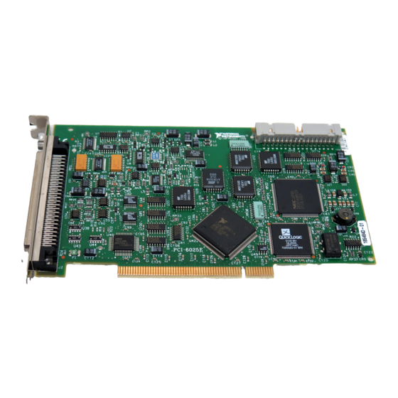
6023E/6024E/6025E User Manual Multifunction I/O Devices for PCI, PXI , ™ CompactPCI, and PCMCIA Bus Computers 6023E/6024E/6025E User Manual December 2000 Edition Part Number 322072C-01... - Page 2 Sweden 08 587 895 00, Switzerland 056 200 51 51, Taiwan 02 2528 7227, United Kingdom 01635 523545 For further support information, see the Technical Support Resources appendix. To comment on the documentation, send e-mail to techpubs@ni.com © Copyright 1998, 2000 National Instruments Corporation. All rights reserved.
-
Page 3: Important Information
Any action against National Instruments must be brought within one year after the cause of action accrues. National Instruments shall not be liable for any delay in performance due to causes beyond its reasonable control. -
Page 4: Table Of Contents
About This Manual Conventions Used in This Manual...xi Related Documentation...xii Chapter 1 Introduction Features of the 6023E, 6024E, and 6025E...1-1 Using PXI with CompactPCI...1-2 What You Need to Get Started ...1-2 Software Programming Choices ...1-3 National Instruments Application Software ...1-3 NI-DAQ Driver Software ...1-4... - Page 5 Programmable Function Input Connections ... 4-31 DAQ Timing Connections ... 4-32 SCANCLK Signal ... 4-33 EXTSTROBE* Signal ... 4-33 TRIG1 Signal... 4-34 TRIG2 Signal... 4-35 STARTSCAN Signal... 4-36 CONVERT* Signal ... 4-38 AIGATE Signal ... 4-39 SISOURCE Signal... 4-40 6023E/6024E/6025E User Manual ni.com...
- Page 6 Loading Calibration Constants ...5-1 Self-Calibration...5-2 External Calibration ...5-2 Other Considerations ...5-3 Appendix A Specifications Appendix B Custom Cabling and Optional Connectors Appendix C Common Questions Appendix D Technical Support Resources Glossary Index © National Instruments Corporation 6023E/6024E/6025E User Manual Contents...
- Page 7 PCI RTSI Bus Signal Connection... 3-10 Figure 3-6. PXI RTSI Bus Signal Connection... 3-11 Figure 4-1. I/O Connector Pin Assignment for the 6023E/6024E... 4-2 Figure 4-2. I/O Connector Pin Assignment for the 6025E ... 4-3 Figure 4-3. Programmable Gain Instrumentation Amplifier (PGIA) ... 4-10 Figure 4-4.
- Page 8 Pins Used by PXI E Series Device...3-11 Table 4-1. I/O Connector Details...4-1 Table 4-2. I/O Connector Signal Descriptions...4-4 Table 4-3. I/O Signal Summary...4-7 Table 4-4. Port C Signal Assignments...4-23 Table 4-5. Signal Names Used in Timing Diagrams ...4-25 © National Instruments Corporation 6023E/6024E/6025E User Manual Contents...
-
Page 9: About This Manual
I/O, and timing I/O. This manual describes the electrical and mechanical aspects of the PCI-6023E, PCI-6024E, DAQCard-6024E, PCI-6025E, and PXI-6025E boards from the E Series product line and contains information concerning their operation and programming. -
Page 10: Related Documentation
• • • 6023E/6024E/6025E User Manual DAQ-STC Technical Reference Manual National Instruments Application Note 025, Field Wiring and Noise Considerations for Analog Signals PCI Local Bus Specification Revision 2.2 PICMG CompactPCI 2.0 R2.1 PXI Specification Revision 2.0 PC Card (PCMCIA) 7.1 Standard... -
Page 11: Introduction
100-pin connector, and 32 lines of digital I/O. The 6024E features 16 channels of analog input, two channels of analog output, a 68-pin connector and eight lines of digital I/O. The 6023E is identical to the 6024E, except that it does not have analog output channels. -
Page 12: Using Pxi With Compactpci
Damage can result if these lines are driven by the sub-bus. What You Need to Get Started To set up and use your device, you need the following: ❑ 6023E/6024E/6025E User Manual Pins Used by PXI E Series One of the following devices: –... -
Page 13: Software Programming Choices
The LabVIEW Data Acquisition VI Library, a series of virtual instruments for using LabVIEW with National Instruments DAQ hardware, is included with LabVIEW. The LabVIEW Data Acquisition VI Library is functionally equivalent to NI-DAQ software. -
Page 14: Ni-Daq Driver Software
It has an extensive library of functions that you can call from your application programming environment. These functions allow you to use all features of your 6023E/6024E/6025E. NI-DAQ addresses many of the complex issues between the computer and the DAQ hardware such as programming interrupts. -
Page 15: Optional Equipment
To download a free copy of the most recent version of NI-DAQ, click Download Software at Optional Equipment National Instruments offers a variety of products to use with your device, including cables, connector blocks, and other accessories, as follows: •... - Page 16 Chapter 1 Introduction For more information about these products, refer to the National Instruments catalogue or web site or call the office nearest you. 6023E/6024E/6025E User Manual ni.com...
-
Page 17: Installation And Configuration
Installation and Configuration This chapter explains how to install and configure your 6023E, 6024E, or 6025E device. Software Installation Install your software before installing your device. If you are using LabVIEW, LabWindows/CVI, ComponentWorks, or VirtualBench, install this software before installing the NI-DAQ driver software. -
Page 18: Hardware Installation
DMA controller that you can only use if the device is installed in a slot that supports bus arbitration, or bus master cards. National Instruments recommends installing the device in such a slot. The PXI specification requires all slots to support bus master cards, but the CompactPCI specification does not. -
Page 19: Hardware Configuration
The device is installed. You are now ready to configure your hardware and software. Hardware Configuration National Instruments standard architecture for data acquisition and standard bus specifications, makes these devices completely software-configurable. You must perform two types of configuration on the devices—bus-related and data acquisition-related configuration. -
Page 20: Hardware Overview
Hardware Overview This chapter presents an overview of the hardware functions on your device. Figure 3-1 shows a block diagram for the PCI-6023E, PCI-6024E, PCI-6025E, and PXI-6025E. Voltage Analog Analog Mode Input Multiplexer Muxes Calibration Dither Generator PFI / Trigger... -
Page 21: Analog Input
Input modes are programmed on a per channel basis for multimode scanning. For example, you can configure the circuitry to scan 12 channels—four DIFF channels and eight RSE channels. Table 3-1 describes the three input configurations. 6023E/6024E/6025E User Manual Calibration DACs 12-Bit... -
Page 22: Input Range
The value of 1 LSB of the 12-bit ADC; that is, the voltage increment corresponding to a change of one count in the ADC 12-bit count. Note: See Appendix A, Specifications, for absolute maximum ratings. © National Instruments Corporation Table 3-1. Available Input Configurations A channel configured in DIFF mode uses two analog input lines. -
Page 23: Dithering
Figure 3-3d, eliminates both the added noise and the effects of quantization. Dithering has the effect of forcing quantization noise to become a zero-mean random variable rather than a deterministic function of the input signal. 6023E/6024E/6025E User Manual of white ni.com... -
Page 24: Multichannel Scanning Considerations
0 and a gain of 100 to channel 1. When the multiplexer switches to channel 1 and the PGIA switches to a gain of 100, the new full-scale range is ±50 mV. © National Instruments Corporation LSBs LSBs -2.0 -2.0... -
Page 25: Analog Output
(DAC) is interpreted in two’s complement format. Analog Output Glitch In normal operation, a DAC output glitches whenever it is updated with a new value. The glitch energy differs from code to code and appears as distortion in the frequency spectrum. 6023E/6024E/6025E User Manual ni.com... -
Page 26: Digital I/O
You can also control these timing signals by signals generated internally to the DAQ-STC, and these selections are fully software-configurable. Figure 3-4 shows an example of the signal routing multiplexer controlling the CONVERT* signal. © National Instruments Corporation Chapter 3 Signal Connections, for more detailed information. -
Page 27: Programmable Function Inputs
It is important to note that you can use any of the PFI pins as an input by any of the timing signals and that multiple timing signals can use the same PFI simultaneously. This flexible routing 6023E/6024E/6025E User Manual RTSI Trigger <0..6> PFI<0..9>... -
Page 28: Device And Rtsi Clocks
RTSI bus and can receive any of these timing signals. This signal connection scheme is shown in Figure 3-5 for PCI devices and Figure 3-6 for PXI devices. © National Instruments Corporation Chapter 3 6023E/6024E/6025E User Manual... -
Page 29: Figure 3-5. Pci Rtsi Bus Signal Connection
Chapter 3 Hardware Overview 6023E/6024E/6025E User Manual Trigger Clock switch Figure 3-5. PCI RTSI Bus Signal Connection 3-10 DAQ-STC TRIG1 TRIG2 CONVERT* UPDATE* WFTRIG GPCTR0_SOURCE GPCTR0_GATE GPCTR0_OUT STARTSCAN AIGATE SISOURCE UISOURCE GPCTR1_SOURCE GPCTR1_GATE RTSI_OSC (20 MHz) ni.com... -
Page 30: Figure 3-6. Pxi Rtsi Bus Signal Connection
RTSI Clock Reserved Reserved Refer to the for a description of the signals shown in Figures 3-5 and 3-6. © National Instruments Corporation PXI Star (6) PXI Trigger (0..5) PXI Trigger (7) switch Figure 3-6. PXI RTSI Bus Signal Connection Table 3-3. -
Page 31: Signal Connections
Connections that exceed any of the maximum ratings of input or output signals on the devices can damage the device and the computer. Maximum input ratings for each signal are given in the Protection column of Table 4-3. National Instruments is not liable for any damages resulting from such signal connections. -
Page 32: Figure 4-1. I/O Connector Pin Assignment For The 6023E/6024E
11 45 PFI1/TRIG2 10 44 DGND +5 V DGND PFI5/UPDATE* PFI6/WFTRIG DGND PFI9/GPCTR0_GATE GPCTR0_OUT FREQ_OUT Not available on the 6023E Figure 4-1. I/O Connector Pin Assignment for the 6023E/6024E ACH0 AIGND ACH9 ACH2 AIGND ACH11 AISENSE ACH12 ACH5 AIGND ACH14 ACH7... -
Page 33: Figure 4-2. I/O Connector Pin Assignment For The 6025E
© National Instruments Corporation AIGND AIGND ACH0 ACH8 ACH1 ACH9 ACH2 ACH10 ACH3 ACH11 ACH4 ACH12 ACH5 ACH13 ACH6 ACH14 ACH7 ACH15 AISENSE DAC0OUT DAC1OUT RESERVED AOGND DGND DIO0 DIO4 DIO1 DIO5 DIO2 DIO6 DIO3 DIO7 DGND +5 V +5 V... -
Page 34: Table 4-2. I/O Connector Signal Descriptions
Chapter 4 Signal Connections Table 4-2 shows the I/O connector signal descriptions for the 6023E, 6024E, and 6025E. Signal Name Reference AIGND ACH<0..15> AIGND AISENSE AIGND DAC0OUT AOGND DAC1OUT AOGND AOGND DGND DIO<0..7> DGND PA<0..7> DGND PB<0..7> DGND PC<0..7> DGND... - Page 35 PFI3/GPCTR1_SOURCE DGND PFI4/GPCTR1_GATE DGND GPCTR1_OUT DGND © National Instruments Corporation Direction Output scan clock—this pin pulses once for each A/D conversion in scanning mode when enabled. The low-to-high edge indicates when the input signal can be removed from the input or switched to another signal.
- Page 36 GPCTR0_OUT DGND FREQ_OUT DGND Indicates that the signal is active low Not available on the 6023E Not available on the 6023E or 6024E 6023E/6024E/6025E User Manual Direction Input PFI5/Update—as an input, this is one of the PFIs. Output As an output, this is the UPDATE* (AO Update) signal. A...
-
Page 37: Table 4-3. I/O Signal Summary
Table 4-3 shows the I/O signal summary for the 6023E, 6024E, and 6025E. Signal Type and Signal Name Direction ACH<0..15> AISENSE AIGND DAC0OUT (6024E and 6025E only) DAC1OUT (6024E and 6025E only) AOGND DGND DIO<0..7> PA<0..7> (6025E only) PB<0..7> (6025E only) PC<0..7>... -
Page 38: Analog Input Signal Overview
Signal Connections Types of Signal Sources When configuring the input channels and making signal connections, you must first determine whether the signal sources are floating or ground-referenced. 6023E/6024E/6025E User Manual Table 4-3. I/O Signal Summary (Continued) Impedance Protection Input/ (Volts) -
Page 39: Floating Signal Sources
(NRSE), referenced single ended (RSE), and differential (DIFF). With the different configurations, you can use the PGIA in different ways. Figure 4-3 shows a diagram of the PGIA of your device. © National Instruments Corporation Chapter 4 6023E/6024E/6025E User Manual Signal Connections... -
Page 40: Figure 4-3. Programmable Gain Instrumentation Amplifier (Pgia)
Exceeding the maximum input voltage rating can damage the device and the computer. National Instruments is not liable for any damages resulting from such signal connections. The maximum input voltage ratings are listed in the Protection column of Table 4-3. -
Page 41: Analog Input Signal Connections
The following sections discuss the use of single-ended and DIFF measurements and recommendations for measuring both floating and ground-referenced signal sources. Figure 4-4 summarizes the recommended input configuration for both types of signal sources. © National Instruments Corporation Chapter 4 4-11 6023E/6024E/6025E User Manual Signal Connections... -
Page 42: Figure 4-4. Summary Of Analog Input Connections
See text for information on bias resistors. Single-Ended — Ground Referenced (RSE) Single-Ended — Nonreferenced (NRSE) See text for information on bias resistors. 6023E/6024E/6025E User Manual Signal Source Type Floating Signal Source ACH(+) ACH (-) AIGND AIGND AISENSE AIGND Figure 4-4. Summary of Analog Input Connections... -
Page 43: Differential Connection Considerations (Diff Input Configuration)
DIFF signal connections also allow input signals to float within the common-mode limits of the PGIA. © National Instruments Corporation The input signal is low level (less than 1 V). The leads connecting the signal to the device are greater than 3 m (10 ft). -
Page 44: Differential Connections For Ground-Referenced Signal Sources
I/O Connector With this type of connection, the PGIA rejects both the common-mode noise in the signal and the ground potential difference between the signal source and the device ground, shown as V 6023E/6024E/6025E User Manual ACH+ ACH– Input Multiplexers... -
Page 45: Differential Connections For Nonreferenced Or Floating Signal Sources
If you do not use the resistors and the source is truly floating, the source is not likely to remain within the common-mode signal range of the PGIA. The PGIA then saturates, causing erroneous readings. © National Instruments Corporation ACH+ ACH– Input Multiplexers... - Page 46 AIGND. If the source has high output impedance, balance the signal path as previously described using the same value resistor on both the positive and negative inputs; be aware that there is some gain error from loading down the source. 6023E/6024E/6025E User Manual 4-16 ni.com...
-
Page 47: Single-Ended Connection Considerations
© National Instruments Corporation The input signal is high level (greater than 1 V). The leads connecting the signal to the device are less than 10 ft (3 m). -
Page 48: Single-Ended Connections For Floating Signal Sources (Rse Configuration)
If the input circuitry of a device were referenced to ground, in this situation as in the RSE input configuration, this difference in ground potentials appears as an error in the measured voltage. 6023E/6024E/6025E User Manual Input Multiplexers AISENSE –... -
Page 49: Common-Mode Signal Rejection Considerations
6024E and 6025E The analog output signals are DAC0OUT, DAC1OUT, and AOGND. DAC0OUT and DAC1OUT are not available on the 6023E. DAC0OUT is the voltage output signal for analog output channel 0. DAC1OUT is the voltage output signal for analog output channel 1. -
Page 50: Digital I/O Signal Connections
Figure 4-10 shows signal connections for three typical digital I/O applications. Caution Exceeding the maximum input voltage ratings, which are listed in Table 4-2, can damage the DAQ device and the computer. National Instruments is not liable for any damages resulting from such signal connections. 6023E/6024E/6025E User Manual DAC0OUT –... -
Page 51: Figure 4-10. Digital I/O Connections
Digital input applications include receiving TTL signals and sensing external device states such as the state of the switch shown in the Figure 4-11. Digital output applications include sending TTL signals and driving external devices such as the LED shown in Figure 4-11. -
Page 52: Programmable Peripheral Interface (Ppi)
In Figure 4-11, port A of one PPI is configured for digital output, and port B is configured for digital input. Digital input applications include receiving TTL signals and sensing external device states such as the state of the switch in Figure 4-11. Digital output applications include sending 6023E/6024E/6025E User Manual TTL Signal Figure 4-11. -
Page 53: Port C Pin Assignments
Handshaking (Bidirectional Bus) * Indicates that the signal is active low. Subscripts A and B denote port A or port B handshaking signals. © National Instruments Corporation Table 4-4. Port C Signal Assignments Signal Assignments 4-23 Chapter 4 Signal Connections... -
Page 54: Power-Up State
A given DIO line is pulled high at power up. To pull it low on power up with an external resistor, follow these steps: 6023E/6024E/6025E User Manual (approximately +5 VDC) with a 100 kΩ ) whose value gives you a maximum of 0.4 VDC. -
Page 55: Timing Specifications
Type STB* Input Output © National Instruments Corporation Using the following formula, calculate the largest possible load to maintain a logic low level of 0.4 V and supply the maximum driving current: V = I × RL ⇒ RL = V/I where: V = 0.4 V... - Page 56 Internal Internal DATA Bidirectional 6023E/6024E/6025E User Manual Description Acknowledge input—a low signal on this handshaking line indicates that the data written to the port has been accepted. This signal is a response from the external device indicating that it has received the data from your DIO device.
-
Page 57: Mode 1 Input Timing
Data after STB* = 1 RD* = 0 to INTR = 0 RD* = 1 to IBF = 0 All timing values are in nanoseconds. © National Instruments Corporation Description Figure 4-13. Timing Specifications for Mode 1 Input Transfer 4-27... -
Page 58: Mode 1 Output Timing
WR* = 1 to OBF* = 0 ACK* = 0 to OBF* = 1 ACK* Pulse Width ACK* = 1 to INTR = 1 All timing values are in nanoseconds. 6023E/6024E/6025E User Manual Description Figure 4-14. Timing Specifications for Mode 1 Output Transfer 4-28 Minimum Maximum —... -
Page 59: Mode 2 Bidirectional Timing
ACK* = 0 to Output ACK* = 1 to Output Float RD* = 1 to IBF = 0 All timing values are in nanoseconds. © National Instruments Corporation Description Figure 4-15. Timing Specifications for Mode 2 Bidirectional Transfer 4-29 Chapter 4... -
Page 60: Power Connections
Under no circumstances connect these +5 V power pins directly to analog or Caution digital grounds, or to any other voltage source on the device or any other device. Doing so can damage the device and the computer. National Instruments is not liable for damages resulting from such a connection. Timing Connections... -
Page 61: Programmable Function Input Connections
As an input, you can individually configure each PFI pin for edge or level detection and for polarity selection, as well. You can use the polarity selection for any of the 13 timing signals, but the edge or level detection © National Instruments Corporation Source I/O Connector Figure 4-16. -
Page 62: Daq Timing Connections
Figure 4-18 shows a typical pretriggered DAQ sequence. The description for each signal shown in these figures is included in this chapter under the section for each corresponding signal. STARTSCAN Scan Counter 6023E/6024E/6025E User Manual TRIG1 CONVERT* Figure 4-17. Typical Posttriggered Acquisition 4-32... -
Page 63: Scanclk Signal
EXTSTROBE* signal. A 10 of eight pulses in the hardware-strobe mode. Figure 4-20 shows the timing for the hardware-strobe mode EXTSTROBE* signal. © National Instruments Corporation Figure 4-18. Typical Pretriggered Acquisition CONVERT* SCANCLK Figure 4-19. -
Page 64: Trig1 Signal
Figures 4-21 and 4-22 show the input and output timing requirements for the TRIG1 signal. Rising-Edge Polarity Falling-Edge Polarity 6023E/6024E/6025E User Manual V OH V OL = 600 ns or 5 µs Figure 4-20. EXTSTROBE* Signal Timing = 10 ns minimum Figure 4-21. -
Page 65: Trig2 Signal
PFI. The TRIG2 signal is not used in posttriggered data acquisition. The output is an active high pulse with a pulse width of 50 to 100 ns. This output is set to high impedance at startup. © National Instruments Corporation 4-35 6023E/6024E/6025E User Manual... -
Page 66: Startscan Signal
STARTSCAN is 6023E/6024E/6025E User Manual = 10 ns minimum Figure 4-23. TRIG2 Input Signal Timing = 50-100 ns Figure 4-24. -
Page 67: Figure 4-25. Startscan Input Signal Timing
If you select an external CONVERT*, the first external pulse after STARTSCAN generates a conversion. Separate the STARTSCAN pulses by at least one scan period. © National Instruments Corporation after the last conversion in the scan is initiated. This output is = 10 ns minimum Figure 4-25. -
Page 68: Convert* Signal
50 to 150 ns. This output is set to high impedance at startup. Figures 4-27 and 4-28 show the input and output timing requirements for the CONVERT* signal. Rising-Edge Polarity Falling-Edge Polarity 6023E/6024E/6025E User Manual = 10 ns minimum Figure 4-27. CONVERT* Input Signal Timing 4-38 ni.com... -
Page 69: Aigate Signal
AIGATE does not gate them back on until the beginning of the next scan. © National Instruments Corporation 4-39 6023E/6024E/6025E User Manual... -
Page 70: Sisource Signal
The selected edge of the WFTRIG signal starts the waveform generation for the DACs. The update interval (UI) counter is started if you select internally generated UPDATE*. 6023E/6024E/6025E User Manual = 50 ns minimum = 23 ns minimum Figure 4-29. -
Page 71: Update* Signal
The selected edge of the UPDATE* signal updates the outputs of the DACs. In order to use UPDATE*, you must set the DACs to posted-update mode. © National Instruments Corporation Chapter 4 = 10 ns minimum Figure 4-30. -
Page 72: Uisource Signal
Any PFI pin can externally input the UISOURCE signal, which is not available as an output on the I/O connector. The UI counter uses the UISOURCE signal as a clock to time the generation of the UPDATE* 6023E/6024E/6025E User Manual = 10 ns minimum Figure 4-32. UPDATE* Input Signal Timing = 300-350 ns Figure 4-33. -
Page 73: General-Purpose Timing Signal Connections
0. This is true even if another PFI is externally inputting the source clock. This output is set to high impedance at startup. © National Instruments Corporation Chapter 4 = 50 ns minimum = 23 ns minimum Figure 4-34. -
Page 74: Gpctr0_Gate Signal
PFI. This output is set to high impedance at startup. Figure 4-36 shows the timing requirements for the GPCTR0_GATE signal. 6023E/6024E/6025E User Manual = 50 ns minimum = 23 ns minimum Figure 4-35. GPCTR0_SOURCE Signal Timing 4-44 ni.com... - Page 75 You can disable this input so that software can control the up-down functionality and leave the DIO6 pin free for general use. © National Instruments Corporation = 10 ns minimum Figure 4-36. GPCTR0_GATE Signal Timing in Edge-Detection Mode Figure 4-37.
-
Page 76: Gpctr1_Source Signal
6023E/6024E/6025E User Manual = 50 ns minimum = 23 ns minimum Figure 4-38. GPCTR1_SOURCE Signal Timing 4-46 ni.com... - Page 77 This input can be disabled so that software can control the up-down functionality and © National Instruments Corporation = 10 ns minimum Figure 4-39. GPCTR1_GATE Signal Timing in Edge-Detection Mode Figure 4-40.
- Page 78 6023E/6024E/6025E User Manual Source Clock Period Source Pulse Width...
-
Page 79: Freq_Out Signal
• • © National Instruments Corporation Use DIFF analog input connections to reject common-mode noise. Use individually shielded, twisted-pair wires to connect analog input signals to the device. With this type of wire, the signals attached to the CH+ and CH–... -
Page 80: Calibration
In the EEPROM there is a user-modifiable calibration area in addition to the permanent factory calibration area. This means that you can load the CalDACs with values either from the original factory calibration or from a calibration that you subsequently performed. © National Instruments Corporation 6023E/6024E/6025E User Manual... -
Page 81: Self-Calibration
Self-Calibration Your device can measure and correct for almost all of its calibration-related errors without any external signal connections. Your National Instruments software provides a self-calibration method. This self-calibration process, which generally takes less than a minute, is the preferred method of assuring accuracy in your application. -
Page 82: Other Considerations
In this case, it is advisable to account for the nominal gain error of the analog output channel either in software or with external hardware. See Appendix A, Specifications, for analog output gain error information. © National Instruments Corporation 6023E/6024E/6025E User Manual Chapter 5 Calibration... -
Page 83: Appendix A Specifications
Sampling rate ... 200 kS/s guaranteed Input signal ranges ... Bipolar only Input coupling ... DC Max working voltage (signal + common mode) ... Each input should remain © National Instruments Corporation Board Gain (Software-Selectable) (software-selectable per channel) Range ±10 V ±5 V... - Page 84 ±10 °C of external or factory-calibration temperature. One-year calibration interval recommended. The Absolute Accuracy at Full Scale calculations were performed for a maximum range input voltage (for example, 10 V for the ±10 V range) after one year, assuming 100 pt averaging of data. 6023E/6024E/6025E User Manual Signal Powered On ±42...
- Page 85 Input impedance Input bias current ... ±200 pA Input offset current... ±100 pA CMRR (DC to 60 Hz) © National Instruments Corporation Appendix A Pregain error after calibration ... ±12 µV max Pregain error before calibration ... ±28 mV max Postgain error after calibration ...
-
Page 86: Dynamic Characteristics
6024E and 6025E only Output Characteristics Number of channels...2 voltage Resolution ...12 bits, 1 in 4,096 Max update rate Type of DAC ...Double buffered, multiplying 6023E/6024E/6025E User Manual Signal Small (–3 dB) Large (1% THD) , not including quantization) Gain Dither Off 0.5 to 10... - Page 87 Note: Temp Drift applies only if ambient is greater than ±10 °C of previous external calibration. Transfer Characteristics Relative accuracy (INL) Monotonicity... 12 bits, guaranteed after Offset error Gain error (relative to internal reference) © National Instruments Corporation Appendix A Absolute Accuracy % of Reading 24 Hours 90 Days 1 Year 0.0177...
- Page 88 Settling time for full-scale step...10 µs to ±0.5 LSB accuracy Slew rate ...10 V/µs Noise ...200 µV Midscale transition glitch Stability Offset temperature coefficient ...±50 µV/°C Gain temperature coefficient ...±25 ppm/°C 6023E/6024E/6025E User Manual Magnitude...±1.1 V Duration... 2.0 ms Magnitude...±2.2 V Duration... 4.2 µs Magnitude...±45 mV Duration... 2.0 µs , DC to 1 MHz ni.com...
- Page 89 Input high current (V Output low voltage (I Output high voltage (I © National Instruments Corporation Appendix A 6025E ... 32 input/output 6023E and 6024E... 8 input/output Level = 0 V) = 5 V) = 24 mA) = 13 mA) Level = 0 V, 100 kΩ...
- Page 90 Max source frequency...20 MHz Min source pulse duration ...10 ns in edge-detect mode Min gate pulse duration ...10 ns in edge-detect mode Data transfers ...DMA, interrupts, DMA modes ...Scatter-gather 6023E/6024E/6025E User Manual PA<0..7> ...Input (High-Z), PB<0..7>...Input (High-Z), PC<0..7>...Input (High-Z), Counter/timers ...24 bits Frequency scalers ...4 bits...
-
Page 91: Power Requirement
Note Power available at I/O connector ... +4.65 to +5.25 VDC at 1 A Physical Dimensions (not including connectors) © National Instruments Corporation Appendix A Level ... 5.000 V (±3.5 mV) (actual Temperature coefficient ... ±5 ppm/°C max Long-term stability ... ±15 ppm/ available at the I/O connector. -
Page 92: Operating Environment
Note MIL-T-28800E and MIL-STD-810E Method 514. Test levels exceed those recommended in MIL-STD-810E for Category 1, Basic Transportation. 6023E/6024E/6025E User Manual 6023E/6024E ...68-pin male SCSI-II type 6025E...100-pin female 0.05D type A-10 Section 4.5.5.4.1) Half-sine shock pulse, 11 ms duration, 30 g peak,... -
Page 93: Input Characteristics
(signal + common mode) ... Each input should remain Overvoltage protection ACH<0..15> AISENSE FIFO buffer size ... 2048 S Data transfers ... Interrupts, programmed I/O Configuration memory size... 512 words © National Instruments Corporation Appendix A Board Gain (Software-Selectable) Signal Powered On ±42 ±40... - Page 94 ±10 °C of external or factory calibration temperature. Transfer Characteristics Relative accuracy...±0.5 LSB typ dithered, DNL ...±0.75 LSB typ, No missing codes...12 bits, guaranteed Offset error Gain error (relative to calibration reference) 6023E/6024E/6025E User Manual Absolute Accuracy Noise + Quantization (mV) Offset (mV) Single Pt.
- Page 95 Crosstalk... –60 dB, DC to 100 kHz Stability Recommended warm-up time ... 30 min Offset temperature coefficient © National Instruments Corporation Normal powered on ... 100 GΩ in parallel with 100 pF Powered off... 4 kΩ min Overload... 4 kΩ min Gain 0.5, 1.0...
- Page 96 Note: Temp Drift applies only if ambient is greater than ±10 °C of previous external calibration. Transfer Characteristics Relative accuracy (INL) Monotonicity ...12 bits, guaranteed after 6023E/6024E/6025E User Manual Interrupts...1 kHz, system dependent Absolute Accuracy % of Reading 24 Hours...
- Page 97 Settling time for full-scale step ... 10 µs to ±0.5 LSB accuracy Slew rate... 10 V/µs Noise ... 200 µVrms, DC to 1 MHz Midscale transition glitch © National Instruments Corporation After calibration ... ±1.0 mV max Before calibration ... ±200 mV max After calibration ... ±0.01% of output max Before calibration ...
- Page 98 Output high voltage (I Power-on state...Input (High-Z), Data transfers ...Programmed I/O Timing I/O Number of channels...2 up/down counter/timers, Resolution Compatibility ...TTL/CMOS 6023E/6024E/6025E User Manual Level = 0 V) = 5 V) = 24 mA) = 13 mA) Counter/timers ...24 bits Frequency scalers ...4 bits...
- Page 99 Excludes power consumed through V Note Power available at I/O connector ... +4.65 to +5.25 VDC at 0.75 A © National Instruments Corporation Counter/timers ... 20 MHz, 100 kHz Frequency scalers... 10 MHz, 100 kHz Level ... 5.000 V (±3.5 mV) (actual Temperature coefficient ...
- Page 100 I/O connector ...68-position VHDCI female Environment Operating temperature ...0 to 40 °C with a maximum Storage temperature ...–20 to 70 °C Relative humidity ...10 to 95% non-condensing 6023E/6024E/6025E User Manual connector internal device temperature of 70 °C as measured by onboard temperature sensor.
-
Page 101: Custom Cabling
DAQCard-6024E, PCI-6023E, PCI-6024E, PCI-6025E, and PXI-6025E devices. Custom Cabling National Instruments offers cables and accessories for you to prototype your application or to use if you frequently change device interconnections. If you want to develop your own cable, however, use the following guidelines: •... - Page 102 AMP backshell, 0.50 max O.D. cable AMP backshell, 0.55 max O.D. cable Mating connectors and a backshell kit for making custom 68-pin cables are available from National Instruments. Optional Connectors The following table shows the optional connector and cable assembly combinations you can use for each device.
-
Page 103: Figure B-1. 68-Pin E Series Connector Pin Assignments
PFI1/TRIG2 10 44 DGND +5 V DGND PFI5/UPDATE* PFI6/WFTRIG DGND PFI9/GPCTR0_GATE GPCTR0_OUT FREQ_OUT Not available on the 6023E Figure B-1. 68-Pin E Series Connector Pin Assignments Custom Cabling and Optional Connectors ACH0 AIGND ACH9 ACH2 AIGND ACH11 AISENSE ACH12 ACH5... -
Page 104: Figure B-2. 68-Pin Extended Digital Input Connector Pin Assignments
Appendix B Custom Cabling and Optional Connectors Figure B-2 shows the pin assignments for the 68-pin extended digital input connector. 6023E/6024E/6025E User Manual 34 68 33 67 32 66 31 65 30 64 29 63 28 62 27 61 26 60... -
Page 105: Figure B-3. 50-Pin E Series Connector Pin Assignments
41 42 PFI3/GPCTR1_SOURCE 43 44 GPCTR1_OUT 45 46 PFI6/WFTRIG 47 48 PFI8/GPCTR0_SOURCE 49 50 GPCTR0_OUT Not available on the 6023E Figure B-3. 50-Pin E Series Connector Pin Assignments Custom Cabling and Optional Connectors AIGND ACH8 ACH9 ACH10 ACH11 ACH12 ACH13... -
Page 106: Figure B-4. 50-Pin Extended Digital Input Connector Pin Assignments
Appendix B Custom Cabling and Optional Connectors Figure B-4 shows the pin assignments for the 50-pin extended digital input connector. 6023E/6024E/6025E User Manual 11 12 13 14 15 16 17 18 19 20 21 22 23 24 25 26 27 28... -
Page 107: General Information
What is the DAQ-STC? The DAQ-STC is the system timing control application-specific integrated circuit (ASIC) designed by National Instruments and is the backbone of the E Series devices. The DAQ-STC contains seven 24-bit counters and three 16-bit counters. The counters are divided into the following three groups: •... - Page 108 Your NI-DAQ or application software release notes documentation is always the best starting place. What version of NI-DAQ must I have to use my 6023E/6024E/6025E? You must have NI-DAQ for PC Compatibles version 6.5 or higher to use a PCI a PXI device. To use the DAQCard-6024E you must have NI-DAQ for PC compatibles version 6.9 or higher.
- Page 109 CTR VIs will still run. However, there are many differences in the counters between the E Series and other devices; the counter numbers are different, timebase selections are different, and the DAQ-STC counters are © National Instruments Corporation Enable the PFI5 line for output, as follows: •...
- Page 110 Table 4-3, Signal high or logic low state. For example, DIO(0) is in the high impedance state 6023E/6024E/6025E User Manual call in NI-DAQ to configure the output line. By Select_Signal Summary.
- Page 111 Table 4-3, I/O Signal Summary, shows that there is a 50 kΩ pull-up resistor. This pull-up resistor sets the DIO(0) pin to a logic high when the output is in a high impedance state. © National Instruments Corporation 6023E/6024E/6025E User Manual...
- Page 112 Technical Support Resources Web Support National Instruments Web support is your first stop for help in solving installation, configuration, and application problems and questions. Online problem-solving and diagnostic resources include frequently asked questions, knowledge bases, product-specific troubleshooting wizards, manuals, drivers, software updates, and more. Web support is available...
- Page 113 Appendix D Technical Support Resources Worldwide Support National Instruments has offices located around the world to help address your support needs. You can access our branch office Web sites from the Worldwide Offices section of up-to-date contact information, support phone numbers, e-mail addresses, and current events.
- Page 114 < less than – negative of, or minus Ω percent ± plus or minus positive of, or plus square root of +5 V +5 VDC source signal © National Instruments Corporation Value –12 –9 – 6 –3 6023E/6024E/6025E User Manual...
- Page 115 All other addresses are located by adding to the base address. bipolar a voltage range spanning both negative and positive voltages breakdown voltage the voltage high enough to cause breakdown of optical isolation, semiconductors, or dielectric materials. Also see 6023E/6024E/6025E User Manual working voltage. ni.com...
- Page 116 D/A converter—an electronic device, often an integrated circuit, that converts a digital number into a corresponding analog voltage or current DAC0OUT analog channel 0 output signal DAC1OUT analog channel 1 output signal © National Instruments Corporation 6023E/6024E/6025E User Manual Glossary...
-
Page 117: Dithering
DAQ device EEPROM electrically erasable programmable read-only memory—ROM that can be erased with an electrical signal and reprogrammed. Some SCXI modules contain an EEPROM to store measurement-correction coefficients. 6023E/6024E/6025E User Manual ni.com... - Page 118 0 clock source signal GPCTR0_UP_DOWN general purpose counter 0 up down GPCTR1_GATE general purpose counter 1 gate signal GPCTR1_OUT general purpose counter 1 output signal GPCTR1_SOURCE general purpose counter 1 clock source signal © National Instruments Corporation 6023E/6024E/6025E User Manual Glossary...
- Page 119 CPU should suspend its current task to service a designated activity input/output—the transfer of data to/from a computer system involving communications channels, operator interface devices, and/or data acquisition and control interfaces current, output high 6023E/6024E/6025E User Manual ni.com...
- Page 120 R = response, S = stimulus, and K = a constant least significant bit multifunction I/O most significant bit © National Instruments Corporation , used with units of , used with B in quantifying data or 6023E/6024E/6025E User Manual Glossary...
- Page 121 Glossary NI-DAQ National Instruments driver software for DAQ hardware noise an undesirable electrical signal—Noise comes from external sources such as the AC power line, motors, generators, transformers, fluorescent lights, soldering irons, CRT displays, computers, electrical storms, welders, radio transmitters, and internal sources such as semiconductors, resistors, and capacitors.
-
Page 122: Programmable Gain Instrumentation Amplifier
10% and 90% points of a system’s step response root mean square—the square root of the average value of the square of the instantaneous signal amplitude; a measure of signal amplitude © National Instruments Corporation 6023E/6024E/6025E User Manual Glossary... - Page 123 Also called a grounded measurement system. RTSI bus real-time system integration bus—the National Instruments timing bus that connects DAQ devices directly, by means of connectors on top of the devices, for precise synchronization of functions...
- Page 124 (for example, 0 to +10 V) UISOURCE update interval counter clock signal © National Instruments Corporation G-11 6023E/6024E/6025E User Manual Glossary...
- Page 125 (2) a LabVIEW software module (VI), which consists of a front panel user interface and a block diagram program volts, input high volts, input low volts in measured voltage volts, output high volts, output low reference voltage volts, root mean square 6023E/6024E/6025E User Manual G-12 ni.com...
- Page 126 See also © National Instruments Corporation breakdown voltage. G-13 Glossary 6023E/6024E/6025E User Manual...
- Page 127 +5 V signal description (table), 4-4 self-resetting fuse, C-1 82C55A Programmable Peripheral Interface. See PPI (Programmable Peripheral Interface). 6023E/6024E/6025E devices. See also hardware overview; specifications. block diagram, 3-1 features, 1-1 to 1-2 optional equipment, 1-5 to 1-6 requirements for getting started, 1-2 to 1-3...
- Page 128 A-15 AOGND signal analog output signal connections, 4-19 to 4-20 description (table), 4-4 signal summary (table), 4-7 6023E/6024E/6025E User Manual bipolar input, 3-3 block diagrams 6023E/6024E/6025E devices, 3-1 DAQCard-6024E, 3-2 cables. See also I/O connectors. custom cabling, B-1 to B-2...
- Page 129 4-20 to 4-21 signal summary (table), 4-7 DIFF mode description (table), 3-3 recommended configuration (figure), 4-12 © National Instruments Corporation differential connections, 4-13 to 4-16 ground-referenced signal sources, 4-14 nonreferenced or floating signal sources, 4-15 to 4-16 when to use, 4-13 digital I/O.
- Page 130 GPCTR1_OUT signal, 4-47 GPCTR1_SOURCE signal, 4-46 GPCTR1_UP_DOWN signal, 4-47 to 4-49 glitch, analog output, 3-6 GPCTR0_GATE signal, 4-44 to 4-45 6023E/6024E/6025E User Manual GPCTR0_OUT signal description (table), 4-6 general-purpose timing signal connections, 4-45 signal summary (table), 4-8 GPCTR0_SOURCE signal, 4-43 to 4-44...
- Page 131 (table), 3-3 overview, 3-3 installation common questions, C-2 hardware, 2-2 to 2-3 software, 2-1 unpacking 6023E/6024E/6025E, 2-1 INTR signal description (table), 4-26 mode 1 input timing (figure), 4-27 mode 1 output timing (figure), 4-28 mode 2 bidirectional timing (figure), 4-29...
- Page 132 (table), 4-8 PFI5/UPDATE signal description (table), 4-6 signal summary (table), 4-8 PFI6/WFTRIG signal description (table), 4-6 signal summary (table), 4-8 6023E/6024E/6025E User Manual PFI7/STARTSCAN signal description (table), 4-6 signal summary (table), 4-8 PFI8/GPCTR0_SOURCE signal description (table), 4-6 signal summary (table), 4-8...
- Page 133 RD* signal description (table), 4-26 mode 1 input timing (figure), 4-27 mode 2 bidirectional timing (figure), 4-29 © National Instruments Corporation referenced single-ended input (RSE). See RSE (referenced single-ended) mode. requirements for getting started, 1-2 to 1-3 RSE (referenced single-ended) mode...
- Page 134 4-30 to 4-49 DAQ timing connections, 4-32 to 4-40 general-purpose timing signal connections, 4-43 to 4-49 6023E/6024E/6025E User Manual programmable function input connections, 4-31 to 4-32 waveform generation timing connections, 4-40 to 4-43 signal sources, 4-8 to 4-9...
- Page 135 GPCTR0_GATE signal, 4-44 to 4-45 GPCTR0_OUT signal, 4-45 GPCTR0_SOURCE signal, 4-43 to 4-44 GPCTR0_UP_DOWN signal, 4-45 GPCTR1_GATE signal, 4-46 to 4-47 © National Instruments Corporation GPCTR1_OUT signal, 4-47 GPCTR1_SOURCE signal, 4-46 GPCTR1_UP_DOWN signal, 4-47 to 4-49 overview, 4-30 programmable function input...
- Page 136 4-40 to 4-43 UISOURCE signal, 4-42 to 4-43 UPDATE* signal, 4-41 to 4-42 WFTRIG signal, 4-40 to 4-41 Web support from National Instruments, D-1 WFTRIG signal, 4-40 to 4-41 Worldwide technical support, D-2 WR* signal description (table), 4-26...