Table of Contents
Advertisement
Advertisement
Table of Contents

Related Manuals for Technics SJ-HD501


Summary of Contents for Technics SJ-HD501
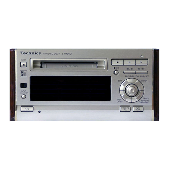
- Page 1 ORDER No.AD9907180C2 Mini Disc Deck SJ-HD501 Mechanism unit: MR3A (RAJ3402) Mechanism Series Colour (N)....Gold Type Areas EG....Europe. EB....Great Britain. This product is option for systems of SC-HD301 and SC-HD501. SPECIFICATIONS...
- Page 2 Specifications Minidisc digital audio system •System Magnetic field modulation Recording direct overwrite Non-contact optical system Reading with Semiconductor laser (=780nm) 44.1 kHz Sampling frequency: ATRAC Cording system: 2channel, stereo Channel: 10-20000Hz (±0.3dB) Frequency response: 90dB S/N Ratio (PLAY): Below measurable limit Wow and flutter: •Input Analog input...
- Page 3 1. Accessories AC power supply cord....1pc. Optical cable....1pc. (RJL1X001B05D)
- Page 4 Remote control batteries....2pcs. [R6/LR6 (AA, UM-3) ] Note:These are available on sales route. Stereo phono cables....2pcs. (RJL2P004B08) Remote control transmitter....1pc. (EUR645272)
- Page 5 2. Precation of Laser Diode...
-
Page 6: Operating Instructions
3. Caution for AC Main Lead 4. Operating Instructions 5. Handling Precautions for Traverse Deck (MD Unit) The laser diode in the MD unit (optical pickup) may break down due to potential difference caused by static electricity of clothes or human body.So, be careful of... - Page 7 electrostatic breakdown during repair of the MD unit (optical pickup). 5.1. Handling of MD Unit (optical pickup) 1. Do not subject the MD unit (optical pickup) to static electricity as it is extremely sensitive to electrical shock. 2. The short land between the No. 25 (LD-GND) and No. 24 (LD) pins on the flexible board is shorted with a solder build-up to prevent damage to the laser diode.
- Page 8 5.2. Grounding for electrostatic breakdown prevention 1. Human body grounding Use the anti-static wrist strap to discharge the static electricity from your body. (As shown in Fig. 2. Work table grounding Put a conductive material (sheet) or steel sheet on the area where the optical pickup is placed, and ground the sheet.
- Page 9 Procedures...
- Page 15 7. Self-Diagnostic Function This unit is equipped with a self-diagnostic function which, in the event of a malfunction, automatically display a code indicating the nature of the malfunction. Use this self-diagnostic function when servicing the unit. 7.1. Switching to the Self-Diagnostic Mode 1.
- Page 16 Fig.2...
- Page 17 8. Self Check Function This unit is equipped with a self check function which can detect a part of malfunction. Use this function before servicing the unit and check the item as shown below. 8.1. Setting to the Self Check Function 1.
- Page 18 Fig.4 Fig.5 8.3. Checking the FL display 1. Press the INPUT SELECTOR button. 2. All buttons works normally except the POWER button, FL display and LED turns on and off at 0.5 second interval. (Refer to Fig.6 and Fig.7.) Fig.6...
- Page 19 Fig.7 The Self Check Function can be canceled by pressing and holding the STOP button for at least 2 seconds. 9. Measurements and Adjustments (Laser Power Adjustment) Note: If you exchange parts of MD unit when you repair, you must perform the Laser Power adjustment.
- Page 20 Because this unit uses the optical magnetic recording, the unit outputs over 10 times more laser than a CD player does. In the adjustment mode, the laser is always being output. Therefore, be especially careful not to look laser beam directly or to touch the laser beam when adjusting the unit and checking its operation.
- Page 21 Cautions 1. About handling the MD unit - The magnetic head is a precision unit and is very fragile. Do not deform it. - Laser diode in the optical pickup may be destroyed by the staticelectricity generated in your clothes or body. Be especially careful with the static electricity.
- Page 22 The optical pickup and the magnetic head are structured precisely; therefore, they are very fragile. Be careful not to touch them with the edge of the laser power meter. The sensor of the laser power meter is a very fine part. Be careful not to touch it to the optical pickup lens.
- Page 23 mechanism. (Refer to Fig.11.) Caution: Do not allow the laser power meter to come in contact with either the optical pickup or the magnetic head. Fig.10 Fig.11...
- Page 24 4. Confirm that the reading of the laser power meter or cartridge type laser power meter is within the specified. If it is not within the specified range, adjust by turning VR1. (Refer to Fig.12.) Specified range (read power): 600µ µ µ µ W or lower Fig.12...
- Page 25 Caution: - Proceeding on to the subsequent adjustment procedure with the read power exceeding 680µ µ µ µ W will result in damage to the optical pickup. 5. Press “2” on the player’s remote control. “WRITE LASER” will be displayed to indicate the write power adjustment mode. 6.
-
Page 26: Troubleshooting Guide
- If the reading in either step 8 or 10 above is not within the specified range, first switch off the power, and then reset the unit to the adjustment mode and repeat the adjustment procedure. 10. Troubleshooting Guide Please refer to this Troubleshooting Guide when you repair for any troubles of this unit. - Page 34 11. Schematic Diagram Notes 11.1. Schemtic Diagram Notes This schematic diagram may be modified at any time with the development of new technology. Notes: S1 : PROTECT det. switch.
- Page 35 S2 : REFLECT det. switch. S3 : LOAD OPEN det. switch. S4 : DISC IN det. switch. S5 : LOAD PLAY/REC det. switch. S6 : LOAD PLAY det. switch. S7 : LOAD TRG det. switch. S8 : Traverse det. switch. S901 : Standby/on ( ) switch.
- Page 36 VR1: Laser power adj. V.R.. VR901 : Input level/Jog push set V.R.. Indicated voltage values are the standard values for the unit measured by the DC electronic circuit tester (high-impedance) with the chassis taken as standard. Therefore, there may exist some errors in the voltage values, depending on the internal impedance of the DC circuit tester.
- Page 37 12. Schematic Diagram 13. Printed Circuit Board 14. Block Diagram 15. Wiring Connection Diagram 16. Terminal Function of IC's 16.1. IC1 (AN8772FHQ) : RF AMP...
- Page 38 Mark Function Division CENVD — D signal det. capacitor connection terminal Laser amp output terminal APCPD Photo diode light quantity det. input terminal LD IN Laser amp reverse input terminal APC REF APC amp criterion voltage input terminal TEMP IN Temperature sensor amp input terminal TEMP...
- Page 39 Mark Function Division Power supply terminal (+3V) 27 NRFDET/ NRFDET/off track signal output terminal OFTR NRFLD Serial command latch signal input terminal 29 RF DATA Serial command data signal input terminal RFCK Serial command clock input terminal 31 NRFSTBY Standby control signal input terminal OUT RF EFM signal output terminal...
- Page 40 Mark Function Division REG B — 3.3V external transistor control terminal (Not used, open) REG M — 3.3V regular output monitor terminal (Not used, connected to GND) — Not used, open Op-amp output terminal Op-amp invert output terminal Op-amp non-invert output terminal (Not used, connected to GND) Power supply terminal...
- Page 41 terminal Mark Function Division Power cut 2 input terminal Focus drive input terminal Tracking drive input terminal 16.3. IC3 (M6616RA1) : ATRAC ENCORDER/DECORDER, SERVO SIGNAL PROCESSOR Mark Function Division ADIP ADIP FM signal input terminal Lens position signal input terminal Focus error signal input terminal Tracking error signal input...
- Page 42 Mark Function Division Focus drive signal output terminal Tracking drive signal output terminal Traverse motor drive signal ouutput terminal Spindle motor drive signal output terminal SPON Drive IC spindle ON signal output terminal TVON Drive IC traverse ON signal output terminal Power supply terminal DV DD 0 FG input terminal...
- Page 43 Mark Function Division SGSYNC Frame synchronous signal output terminal DVDD1 Power supply terminal IVDD1 — Power supply terminal for I/O pad DVss1 — GND terminal FS384 384 Fs output terminal Bit clock output terminal Word clock output terminal SDAP Audio data output terminal SDAR Audio data input terminal LRCK...
- Page 44 Mark Function Division 82 EXSYSCK — External system clock input terminal (Not used, connected to GND) DVDD2 Power supply terminal Crystal oscillator input terminal (F=16.9344MHz) Crystal oscillator output terminal (F=16.9344MHz) VDss2 — GND terminal RFDAT RF serial data output terminal RFCK RF serial clock output terminal...
- Page 45 Mark Function Division DACRST DAC reset signal output terminal to IC4 (“L”:Reset) DE emphasis signal output terminal to IC4(“L”:DE emphases) MUTE — AD-DA mute output terminal (Not used, open) AD RST Reset signal output terminal Standby control signal NRFSTBY output terminal (“L”:Standby) Transistor drive signal output terminal (“H”:Power...
- Page 46 MMOD — Connected to GND...
- Page 47 Mark Function Division Reset signal input terminal (“L”:Reset) UNIT Test signal input terminal TEST (Open) Test signal input terminal (Open) SCTSY Micro computer interrupt signal input terminal (SUBQ/ADIP simultaneous signal) MDISY Micro computer interrupt signal input terminal (MD simultaneous signal) PANEL Panel I/F request signal input terminal...
- Page 48 input terminal Mark Function Division TEST06 Test signal output terminal (Not used, open) TEST07 Connected to rec/play switch signal TOK OK Not used, open HF ON — Drive signal output terminal to Q3 (POWER SUPPLY CONTROL) PANEL Panel I/F clock input terminal PANEL Panel I/F data input terminal...
- Page 49 Mark Function Division TEST Test signal input terminal KEY IN (“L”:Unit key mode) (Open) Test signal input terminal LOAD (“L”:Using for servo primary values EEPROM) VCC 3V Power supply terminal (+3V) VCC 5V Power supply terminal (+5V) 71 SELADDA AD/DA converter select signal input terminal (Open) SLOCK Spindle lock test signal...
- Page 50 Mark Function Division DRAM data 1 in/output terminal DRAM data 2 in/output terminal DRAM light enable input terminal DRAM low address strobe input terminal DRAM address 9 input terminal DRAM address 0 input terminal DRAM address 1~3 input terminal Power supply terminal DRAM address 4~8 input terminal DRAM output enable input...
- Page 51 Mark Function Division VR control clock output terminal VR control data output terminal VR control STB output terminal Digital in 1/2 select signal output terminal (“H”: in 1) Not used, connected to Chip select input terminal Request signal output terminal Reset signal output terminal CNVSS...
- Page 52 Mark Function Division Not used, connected to power supply through ~P70 resistor — Not used, connected to power supply through ~P44 resistor — Not used, connected to Model select terminal FL segment control signal output terminal ~P30 ~P10 Power supply input terminal FL segment control signal output terminal...
- Page 53 Mark Function Division AVSS — GND terminal P100/ — Not used, connected to VREF Referance voltage input terminal AVCC Power supply input terminal 17. Replacement Parts List Notes: *Important safety notice: Components identified by mark have special characteristics important for safety. Funrthermore, special parts which have purposes of fire-retardant (resistors), high-quality sound (capacitors), low-noise (resistors), etc.
- Page 54 Part No. Ref. No. Part Name & Description Remarks SIDE PANEL(L) RGK1148-M RGK1149-M SIDE PANEL(R) RHD30073-K SCREW RKM0326G-S CABINET [MAVD] XTBS3+8JFZ1 SCREW REZ1250 FFC(30P) [MAVD] REZ1251 FFC(20P) [MAVD] RKA0076-N3 FOOT RKA0083-K CUSHION XTB3+6G SCREW RGK0810-N3 SIDE ORNAMENT(L) RGK0811-N3 SIDE ORNAMENT(R) RGK0886-1H MD LID RGL0345-Q...
- Page 55 Part No. Ref. No. Part Name & Description Remarks XTN17+6GFZ SCREW RMR1118-K2 HOLDER EUR645272 REMOTE CONTROLLER [MAVD] A1-1 UR64EC1987B BATT.COVER(REMOTE CONT.) 1 RJA0044-C AC POWER SUPPLY CORD (EB)[MAVD] RJA0043-C AC POWER SUPPLY CORD (EG) RJL1X001B05D OPTICAL CABLE RJL2P004B08A RCA PIN CORD RQA0117 WARRANTY CARD RQCB0169...
- Page 56 Part No. Ref. No. Part Name & Description Remarks ECUV1C823KBV 16V 0.082U ECEV1CA100NR 16V 10U ECUVNJ334KBV 63V 0.33U ECUV1H221KBV 50V 220P ECUVNE153KBV 25V 0.015U ECUVNC104KBV 16V 0.1U ECUV1C823KBV 16V 0.082U ECUV1H392KBV 50V 3900P ECUV1E123KBV 25V 0.012U C71-76 ECUVNC104ZFV 16V 0.1U C79,80 ECUVNC104ZFV 16V 0.1U...
- Page 57 Part No. Ref. No. Part Name & Description Remarks C307 ECUV1H102KCN 50V 1000P C308 ECEA1HKA220B 50V 22U C309 ECBT1H104ZF5 50V 0.1U C311,12 ECA1EM471 25V 470U C313,14 ECUVNE104ZFN 25V 0.1U C315,16 ECEA1AKS470 10V 47U C317,18 ECA1AM221B 10V 220U C321 ECUV1E104KBN 25V 0.1U C322 ECEA0JKS101 6.3V 100U...
- Page 58 Part No. Ref. No. Part Name & Description Remarks CP404 RJU057W007 CONNECTOR(7P) D5,6 SC80209TE12R DIODE MA728TX DIODE D301-07 1D3-E DIODE D308 MA4270H DIODE D309,10 1D3-E DIODE D311,12 MA4091M DIODE D313,14 MA4051M DIODE D315 MA4062M DIODE D316 MA4056M DIODE D317,18 1SS291TA DIODE D319,20 MA110TX...
- Page 59 L4 8 RLQU2R2MT W COIL...
- Page 60 Part No. Ref. No. Part Name & Description Remarks L9-12 RLQU100KT-W COIL L13,14 RLQU2R2MT-W COIL RLQU100KT-W COIL RLQU2R2MT-W COIL L17,18 RLQP1R8KT2-Y COIL L201,02 SLQX400-D COIL RPF0139 PROTECTION BAG(F.B.) RPG4525 PACKING CASE [MAVD] RPN1008 CUSHION RPQ0981 [MAVD] PCB1 REP2878AB-S POWER P.C.B. <RTL>[MAVD] PCB2 REP2878AA-S...
- Page 61 Part No. Ref. No. Part Name & Description Remarks ERJ3GEYJ472V 1/16W 4.7K ERJ3GEYJ271V 1/16W 270 ERJ3GEYJ474V 1/16W 470K ERJ3GEYJ101V 1/16W 100 ERJ3GEYJ223V 1/16W 22K ERJ6GEYJ3R3V 1/8W 3.3 ERJ3GEYD103V 1/16W 10K ERJ3GEYJ223V 1/16W 22K ERJ3GEYJ104Z 1/16W 100K ERJ3GEYJ223V 1/16W 22K ERJ3GEYJ103Z 1/16W 10K ERJ3GEYJ102Z 1/16W 1K...
- Page 62 Part No. Ref. No. Part Name & Description Remarks ERJ3GEYJ223V 1/16W 22K R86,87 ERJ3GEYJ102Z 1/16W 1K R89,90 ERJ3GEYJ102Z 1/16W 1K ERJ3GEYJ102Z 1/16W 1K ERJ3GEYJ222V 1/16W 2.2K R98,99 ERJ3GEYJ102Z 1/16W 1K R100 ERJ3GEYJ473V 1/16W 47K R103 ERJ3GEYJ102Z 1/16W 1K R104,05 ERJ3GEYJ272V 1/16W 2.7K R107-10 ERJ3GEYJ102Z...
- Page 63 Part No. Ref. No. Part Name & Description Remarks R711,12 ERJ6GEYJ561V 1/10W 560 R713,14 ERJ6GEYJ473V 1/10W 47K R715,16 ERJ6GEYJ472V 1/10W 4.7K R717,18 ERJ6GEYJ682V 1/10W 6.8K R719,20 ERJ6GEYJ333V 1/10W 33K R721,22 ERJ6GEYJ683V 1/10W 68K R723,24 ERJ6GEYJ154V 1/10W 150K R725,26 ERJ6GEYJ331V 1/10W 330 R727-30 ERJ6GEYJ151V 1/10W 150...
- Page 64 Part No. Ref. No. Part Name & Description Remarks RSH1A045-A SW LOAD TRG RSP1A023-A SW,TV S901-15 EVQ21405R SW PUSH T201 RTP1K4B034-V POWER TRANSFORMER [MAVD] RRSP33J103CW THERMISTOR EVM3YSX50B14 VR LASER POWER ADJ. VR901 RRV11B152A-A VR ENCODER RSXY10M0M02T OSCILLATOR RSXC16M9S03T OSCILLATOR X901 EF0MC1005L4 CERALOCK ELEMENT [MAVD]...
- Page 65 (For United Kingdom) WARNING: DO NOT CONNECT EITHER WIRE TO (“EB” area code model only) THE EARTH TERMINAL WHICH IS MARKED WITH THE LETTER E, BY THE EARTH SYMBOL n n OR CO- For your safety, please read the following text careful- LOURED GREEN OR GREEN/YELLOW.