Table of Contents
Advertisement
SERVICE MANUAL
HCD-VX8/VX8J is the tuner, deck, CD and
amplifier section in MHC-VX8/VX8J.
MICROFILM
HCD-VX8/VX8J
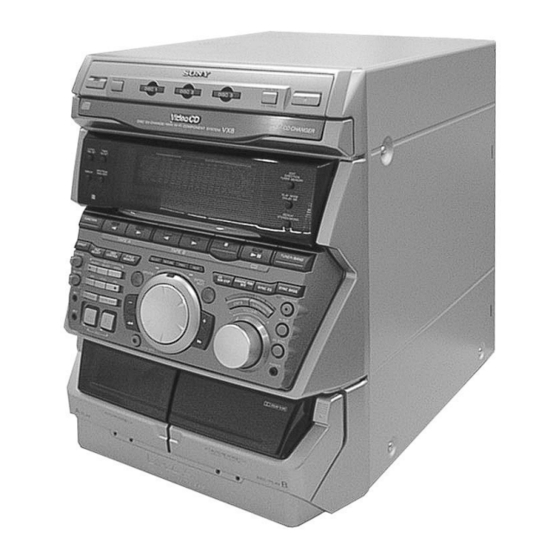
Photo: HCD-VX8 (SILVER)
Model Name Using Similar Mechanism HCD-GRX80/RXD8/RXD8S
CD
CD Mechanism Type
SECTION
Base Unit Type
Optical Pick-up Type
Model Name Using Similar Mechanism HCD-GRX80/RXD8/RXD8S
TAPE DECK
SECTION
Tape Transport Mechanism Type
SPECIFICATIONS
COMPACT DISC DECK RECEIVER
– 1 –
E Model
CDM38L-5BD34L
BU-5BD34L
KSS-213D/Q-NP
TCM-230AWR2/230PWR2
— Continued on next page —
Advertisement
Table of Contents

Related Manuals for Sony HCD-VX8


Summary of Contents for Sony HCD-VX8
- Page 1 HCD-VX8/VX8J SERVICE MANUAL E Model HCD-VX8/VX8J is the tuner, deck, CD and Photo: HCD-VX8 (SILVER) amplifier section in MHC-VX8/VX8J. Model Name Using Similar Mechanism HCD-GRX80/RXD8/RXD8S CD Mechanism Type CDM38L-5BD34L SECTION Base Unit Type BU-5BD34L Optical Pick-up Type KSS-213D/Q-NP Model Name Using Similar Mechanism HCD-GRX80/RXD8/RXD8S...
- Page 2 REPLACE THESE COMPONENTS WITH SONY PARTS Carry out the “S curve check” in “CD section adjustment” and check WHOSE PART NUMBERS APPEAR AS SHOWN IN THIS that the S curve waveform is output four times. MANUAL OR IN SUPPLEMENTS PUBLISHED BY SONY. – 2 –...
-
Page 3: Table Of Contents
TABLE OF CONTENTS 1. SERVICING NOTE 9. EXPLODED VIEWS ............4 9-1. Case Section ................ 90 9-2. Chassis Section ..............91 2. GENERAL ................5 9-3. Front Panel Section ............. 92 9-4. CD Mechanism Deck Section-1 (CDM38L-5BD34L) ..93 3. DISASSEMBLY 9-5. -
Page 4: Servicing Note
SECTION 1 SERVICING NOTE HOW TO OPEN THE DISC TRAY WHEN POWER SWITCH TURNS OFF 1 Remove the Case. 3 Pull-out the disc tray. 2 Turn the cam to the direction of arrow. NOTE FOR INSTALLATION (ROTARY ENCODER) Note:When attaching the Base unit, Insert the BU cam section A into the groove of BU cam. -
Page 5: General
SECTION 2 GENERAL Front Panel 12 13 14 16 17 20 21 40 39 30 29 LOCATION OF PARTS AND CONTROLS 1 1/u (Power) button and indicator 21 SURROUND button 43 BEAT SPEED button 22 HI DUB button 44 BEAT SELECT button 2 DEMO (STANDBY) button 45 BEAT ON/OFF button and indicator 3 DISC 1 button and indicator... -
Page 7: Disassembly
SECTION 3 DISASSEMBLY Note: Follow the disassembly procedure in the numerical order given. 3-1. LOADING PANEL Claws 3 Loading panel 1 Turn the cam to the direction of arrow. 2 Pull-out the disc tray. 3-2. FRONT PANEL AND VIDEO BOARD !∞... -
Page 8: Cassette Lid And Tape Mechanism
3-3. CASSETTE LID AND TAPE MECHANISM 9 Tape mechanism 8 Three screws (BVTP2.6x8) 7 Two screws (BVTP2.6x8) 6 Tension spring 4 Cassette holder (L) assembly Note for installation Portion A 2 Release (Refer to order No. 1 ) Portion A 3 Cassette holder (R) assembly 5 Tension spring... -
Page 9: Disc Tray
3-5. DISC TRAY (Perform after removing the front panel.) Note:When installing the Disc tray, pull around the flat type wire to pass through the claw A and claw B , as shown in the figure. 3 Flat type wire (8 core) 4 Two claws 2 Pull-out the disc tray. -
Page 10: Service Mode
SECTION 4 SERVICE MODE MC Cold Reset • The cold reset clears all data including preset data stored in the RAM to initial conditions. Execute this mode when returning the set to the customer. Procedure: 1. Press three buttons p , ENTER/NEXT , and 1/u simultaneously. 2. - Page 11 AMS Test Mode • This mode is used for checking the AMS operations of the tape deck. 7-819-039-12 Alignment tape, AMS-110A Procedure: 1. Press the 1/u button to turn the unit ON. 2. Set the tape (AMS-110A). 3. Press the three buttons p , ENTER/NEXT , and DISC 3 button simultaneously. 4.
-
Page 12: Test Mode
SECTION 5 TEST MODE VIDEO CD COLOR-BARS MODE On this mode, the data of the color-bars signal as a picture signal and the 1kHz sine wave signal as a sound signal are output by the mechanism control microcomputer (IC502) for video CD signal check. When measurement of the voltage and waveform on the VIDEO board, perform it in this mode. -
Page 13: Mechanical Adjustments
SECTION 6 SECTION 7 MECHANICAL ADJUSTMENTS ELECTRICAL ADJUSTMENTS Precaution DECK SECTION 0 dB=0.775V 1. Clean the following parts with a denatured alcohol-moistened swab: 1. Demagnetize the record/playback head with a head damagnetizer. record/playback heads pinch rollers 2. Do not use a magnetized screwdriver for the adjustments. erase head rubber belts 3. - Page 14 3. Mode: Playback Tape Speed Adjustment (Deck A) test tape Note: Set the test mode using the following method and begin tape P-4-A100 speed adjustment. (10kHz, –10dB) oscilloscope In the test mode, the speed will switch to double speed or normal speed each time the HI DUB button is pressed.
- Page 15 Record Bias Adjustment (Deck B) Record Level Adjustment (Deck B) Procedure: Procedure: INTRODUCTION INTRODUCTION When set to the test mode performed in Tape Speed Adjust- When set to the test mode performed in Tape Speed Adjust- ment, when the tape is rewound after recording, the “REC memory ment, when the tape is rewound after recording, the “REC memory mode”...
- Page 16 Note: Clear RF signal waveform means that the shape “◊” can be CD SECTION clearly distinguished at the center of the waveform. Note: RF signal waveform 1. CD Block is basically constructed to operate without adjustment. Therefore, check each item in order given. VOLT/DIV : 200mV 2.
- Page 17 Adjustment Location : [ BD BOARD ] — SIDE B — (RF) (VC) (TE) (FE) (AGCCON) (IOP) VIDEO SECTION Frequency adjustment frequency counter 1. Connect the frequency counter to check point of the VIDEO VIDEO board board. (29 MHz) 2. Adjust CT503 of the VIDEO board so that the frequency counter –...
-
Page 18: Diagrams
SECTION 8 DIAGRAMS 8-1. CIRCUIT BOARDS LOCATION VIDEO board CD SW board ENCAPSULATED COMPONENT (EXCEPT THAI) PANEL board TUNER unit (THAI) TRANS board SURROUND board MAIN board ENCAPSULATED COMPONENT/TUNER unit is supplied as the assembled block. MOTOR (TURN) board CONNECTOR board BD board SENSOR board MOTOR (SLIDE) board... -
Page 19: Block Diagrams
HCD-VX8/VX8J 8-2. BLOCK DIAGRAMS – CD SECTION – IC381 OPTICAL PICK-UP BLOCK CD DIGITAL (D/Q-Np) IC101 D+5V OPTICAL DIGITAL SERVO DETECTOR IC103 DIGITAL SIGNAL PRCESSOR RF AMP DIGITAL D OUT ERROR DOUT CORRECTOR PCM-D RF AC RF EQ REGISTER ADATA... -
Page 20: Video Section
HCD-VX8/VX8J – VIDEO SECTION – D-RAM IC507 IC506 16 - 19 22 - 26 2 - 10 31 - 39 13 - 15 17 - 21 25 4 28 29 3 2 14 10 12 - 5 27 26 23... -
Page 21: Deck Section
HCD-VX8/VX8J – DECK SECTION – PB A/B S1008 S1004 MS OUT A CrO B CrO RV311 MAIN SECTION 28 27 PLAYBACK IC611 A 120/70 LEVEL PB-A/B B 120/70 DECK A A IN PB OUT B IN PB L HP101 PB HEAD... -
Page 22: Power Section
HCD-VX8/VX8J ECHO PROCESSOR IC711 LPF 1 IN LPF 2 OUT – MAIN SECTION – RV712 ECHO LEVEL J711 LEVEL R-CH IC712(1/2) (Page 30) SPE SIG IC712(2/2) WAKE UP DISPLAY IC181(2/2) IC181(1/2) SECTION STANDBY LED MUTE DJ-SIG DISPLAY IIC DATA Q181... - Page 23 HCD-VX8/VX8J – POWER SECTION – TM402 F RELAY SURROUND • R CH : Same as L ch SPEAKER • SIGNAL PATH THERMAL : FM • Abbreviation POWER AMP Q831, 832 IC801 THP831 : Saudi Arabia model. FAN MOTOR M901 RY401 : Singapore model.
-
Page 24: Display Section
HCD-VX8/VX8J – DISPLAY SECTION – D637 RIGHT LED SWITCH +5V (LED) Q607 LED SWITCH GRADATION L Q608 D638 LEFT IC604 • Q601,602 L/P SCK LED LA +5V (LED) PANEL LED SWITCH • L/P DAT • IIC DATA C DATA IIC CLK... - Page 25 HCD-VX8/VX8J WAVEFORMS – VIDEO SECTION – – MAIN (3/4) SECTION – THIS NOTE IS COMMON FOR PRINTED WIRING – CD SECTION – BOARDS AND SCHEMATIC DIAGRAMS. (In addition to this, the necessary note is printed in each block.) 4Vp-p 5.2Vp-p 5.8Vp-p...
-
Page 26: Printed Wiring Board - Cd Section
HCD-VX8/VX8J 8-3. PRINTED WIRING BOARD – CD SECTION – • See page 18 for Circuit Boards Location. (Page 42) – 33 – – 34 –... -
Page 27: Schematic Diagram - Cd Section
HCD-VX8/VX8J 8-4. SCHEMATIC DIAGRAM – CD SECTION – • See page 31 for Waveforms. • See page 77 for IC Block Diagrams. • See page 80 for IC Pin Functions. (Page 43) – 35 – – 36 –... -
Page 28: Schematic Diagram - Deck Section
HCD-VX8/VX8J 8-5. SCHEMATIC DIAGRAM – DECK SECTION – (Page 55) – 37 – – 38 –... -
Page 29: Printed Wiring Board - Deck Section
HCD-VX8/VX8J 8-6. PRINTED WIRING BOARD – DECK SECTION – • See page 18 for Circuit Boards Location. (Page 49) – 39 – – 40 –... -
Page 30: Printed Wiring Board - Video Section
HCD-VX8/VX8J 8-7. PRINTED WIRING BOARD – VIDEO SECTION – • See page 18 for Circuit Boards Location. (Page 50) (Page 34) • Semiconductor • Semiconductor Location Location Ref. No. Location Ref. No. Location D301 IC501 D501 IC502 D502 IC506 IC101... -
Page 31: Schematic Diagram - Video (1/3) Section
HCD-VX8/VX8J 8-8. SCHEMATIC DIAGRAM – VIDEO (1/3) SECTION – • See page 32 for Waveforms. • See page 82 for IC Pin Functions. (Page (Page 35) (Page 51) (Page 47) (Page 45) (Page 45) – 43 – – 44 –... -
Page 32: Schematic Diagram - Video (2/3) Section
HCD-VX8/VX8J 8-9. SCHEMATIC DIAGRAM – VIDEO (2/3) SECTION – • See page 31 for Waveforms. • See page 84 for IC Pin Functions. (Page 43) (Page 43) (Page 47) (Page 47) – 45 – – 46 –... -
Page 33: Schematic Diagram - Video (3/3) Section
HCD-VX8/VX8J 8-10. SCHEMATIC DIAGRAM – VIDEO (3/3) SECTION – • See page 32 for Waveforms. • See page 78 for IC Block Diagrams. (Page 44) (Page 44) (Page 46) (Page 46) – 47 – – 48 –... -
Page 34: Printed Wiring Board - Main Section
HCD-VX8/VX8J 8-11. PRINTED WIRING BOARD – MAIN SECTION – • See page 18 for Circuit Boards Location. (Page 71) (Page 42) (Page 71) • Semiconductor Location Ref. No. Location Ref. No. Location D141 E-10 Q113 D191 E-10 Q161 D331 Q162... -
Page 35: Schematic Diagram - Main (1/4) Section
HCD-VX8/VX8J 8-12. SCHEMATIC DIAGRAM – MAIN (1/4) SECTION – (Page (Page 43) (Page (Page 70) (Page 70) (Page 57) (Page 55) (Page 56) (Page 76) – 51 – – 52 –... -
Page 36: Schematic Diagram - Main (2/4) Section
HCD-VX8/VX8J 8-13. SCHEMATIC DIAGRAM – MAIN (2/4) SECTION – • See page 49 for Printed Wiring Board. (Page (Page (Page (Page (Page (Page 57) (Page 57) (Page 58) (Page 58) – 53 – – 54 –... -
Page 37: Schematic Diagram - Main (3/4) Section
HCD-VX8/VX8J 8-14. SCHEMATIC DIAGRAM – MAIN (3/4) SECTION – • See page 32 for Waveforms. • See page 49 for Printed Wiring Board. • See page 87 for IC Pin Functions. (Page 51) (Page 52) (Page 53) (Page (Page (Page... -
Page 38: Schematic Diagram - Main (4/4) Section
HCD-VX8/VX8J 8-15. SCHEMATIC DIAGRAM – MAIN (4/4) SECTION – • See page 49 for Printed Wiring Board. (Page 53) (Page 53) (Page 53, 54) (Page 52) (Page 54) (Page (Page (Page (Page (Page 73) (Page 66) – 57 – – 58 –... -
Page 39: Printed Wiring Board - Leaf Sw Section
HCD-VX8/VX8J 8-16. PRINTED WIRING BOARD – LEAF SW SECTION – • See page 18 for Circuit Boards Location. (Page 49) 8-17. SCHEMATIC DIAGRAM – LEAF SW SECTION – (Page 55) – 59 – – 60 –... -
Page 40: Printed Wiring Board - Panel Section
HCD-VX8/VX8J 8-18. PRINTED WIRING BOARD – PANEL SECTION – • See page 18 for Circuit Boards Location. • Semiconductor Location Ref. No. Location D601 VIDEO CD D608 D609 D611 (Page 49) D612 D613 D614 D615 D616 D617 D618 PBC OFF... -
Page 41: Schematic Diagram - Panel (1/3) Section
HCD-VX8/VX8J 8-19. SCHEMATIC DIAGRAM – PANEL (1/3) SECTION – • See page 77 for IC Block Diagrams. (Page 65) (Page 67) (Page 67) – 63 – – 64 –... -
Page 42: Schematic Diagram - Panel (2/3) Section
HCD-VX8/VX8J 8-20. SCHEMATIC DIAGRAM – PANEL (2/3) SECTION – • See page 34 for Waveforms. • See page 61 for Printed Wiring Board. • See page 78 for IC Block Diagrams. • See page 89 for IC Pin Functions. (Page 57) -
Page 43: Schematic Diagram - Panel (3/3) Section
HCD-VX8/VX8J 8-21. SCHEMATIC DIAGRAM – PANEL (3/3) SECTION – • See page 61 for Printed Wiring Board. • See page 78 for IC Block Diagrams. (Page 65) (Page 66) (Page 63) (Page 63) – 67 – – 68 –... -
Page 44: Schematic Diagram - Cd Motor Section
HCD-VX8/VX8J 8-22. SCHEMATIC DIAGRAM – CD MOTOR SECTION – 1SS119 (Page 51) MTZJ-T-72-5.6C (M) 1SS119 (Page 51) MTZJ-T-72-3.6C (M) – 69 – – 70 –... -
Page 45: Printed Wiring Board - Cd Motor Section
HCD-VX8/VX8J 8-23. PRINTED WIRING BOARD – CD MOTOR SECTION – • See page 18 for Circuit Boards Location. (Page 49) (Page 50) – 71 – – 72 –... -
Page 46: Schematic Diagram - Trans Section
HCD-VX8/VX8J 8-24. SCHEMATIC DIAGRAM – TRANS SECTION – (Page 54) (Page 57) – 73 – – 74 –... -
Page 47: Printed Wiring Board - Trans Section
HCD-VX8/VX8J 8-25. PRINTED WIRING BOARD – TRANS SECTION – • See page 18 for Circuit Boards Location. 8-26. SCHEMATIC DIAGRAM – SURROUND SECTION – • See page 79 for IC Block Diagrams. (Page 51) 8-27. PRINTED WIRING BOARD – SURROND SECTION –... -
Page 48: Ic Block Diagrams
HCD-VX8/VX8J 8-28. IC BLOCK DIAGRAMS • BD Board • VIDEO (3/3) Board IC103 CXA2568M-T6 • BD Board IC509 PCM1727E-2/T2 384fs IC101 CXD3008Q APC PD AMP LC/PD CLOCK MANAGER • LD_ON DUAL PLL 80 79 78 77 76 75 74 73... - Page 49 • SURROUND Board IC1201 LV1150 R-OUT R-IN VIRTUAL R +DELAY L-IN L-OUT RS-OUT L.P.F L-FS-IN EF-VOL L –DELAY VREF R-PS-IN AGND L +R L –R LS-OUT DC-OUT LPF2 SRAM LPF1 ADM-CONT LC-INB LC-INE – 79 –...
-
Page 50: Ic Pin Functions
8-29. IC PIN FUNCTIONS • IC101 DIGITAL SIGNAL PROCESSOR (CXD3008Q) (BD Board) Pin Name Function Pin No. DVDD0 — Digital power supply XRST System reset MUTE Muting selection pin DATA Serial data input, supplied from CPU XLAT Latch input, supplied from CPU CLOK Serial data transfer clock input, supplied from CPU SENS... - Page 51 Pin No. Pin Name Function Tracking error signal input Center servo analog input RFDC RF signal input ADI0 Test pin (Not used) AVSS0 — Analog ground IGEN Power supply pin operational amplifiers AVDD — Analog power supply ASYO EFM full swing output ASYI Asymmetry comparate voltage input RFAC...
- Page 52 • IC502 MPEG DECODER, MECHANISM CONTROL (M30620MC-A05FP) (VIDEO (1/3) Board) Pin Name Function Pin No. SENSE Internal state (SENSE) monitor input (IC101) SENSE CLK Serial data reading clock output (IC101) DSP DATA Serial data output (IC101) DSP LATCH Lach output (IC101) DSP CLK Serial data clock output (IC101) TSENS...
- Page 53 Pin Name Function Pin No. BUS XWRL Not used LO. BOOST Not used AUDIO MUTE Audio mute output “L” : mute LOAD OUT Not used LOAD IN Not used INSW Not used OUTSW Not used MODEL 1 L : System input (Fixed at “L”) MODEL 2 L : System input (Fixed at “L”) TBLL...
- Page 54 • IC505 CD DECODER, SYSTEM CONTROL (CL680T-D1) (VIDEO (2/3) Board) Pin No. Pin Name Function – Not used – Ground CD-BCK CD Decode bit clock CD-DATA CD Decode data CD-LRCK CD Decode Left or Right channel selection clock CD-C2PO CD Decode C2 error data –...
- Page 55 Pin No. Pin Name Function Address data from CL680 to Microcode ROM/DRAM – Ground Address data from CL680 to Microcode ROM/DRAM VDD3 – +3.3V Power supply Address data from CL680 to Microcode ROM/DRAM Address data from CL680 to Microcode ROM/DRAM Address data from CL680 to Microcode ROM/DRAM –...
- Page 56 Pin Name Function Pin No. PGIO0 Not used PGIO8 Not used PGIO2/VSYNC/CSYNC Vertical synchronized signal of video signal AVDD PLL – +3.3V Power supply – Not used – Not used – Not used AGND PLL – Ground – Ground – Not used PGIO3/HSYNC Not used...
- Page 57 • IC501 MASTER CONTROL (M30622MA-A09FP) (MAIN Board) Function Pin No. Pin Name STK-MUTE Power amp ON/OFF signal output POWER Power ON/OFF signal output F-RELAY Front speaker relay control output REAR-RELAY Rear speaker relay control output (Not used) CD-POWER CD power on signal output LINE-MUTE Line mute ON/OFF selection output DBFB-H/L...
- Page 58 Pin No. Pin Name Function STEREO Stereo detection for tuner TUNED Tuned detection for tuner ST-CE Tuner chip enable output ST-DOUT Tuner data output ST-DIN Tuner data input ST-CLK Tuned clock output SENS BD Condition signal input (Not used) HDLD Mode hold signal output (Not used) CD latch signal output (Not used) XRST...
- Page 59 • IC601 DISPLAY CONTROL (TMP88CS76F-6005) (PANEL Board) Pin Name Function Pin No. SIRCS Remote commander signal input JOG A Rotary encoder (S601) pulse input L/P SCK LED/PAD clock output LED LA LED latch output L/P DAT LED/PAD data output PAD LA PAD latch output L SEL LED select signal...
-
Page 60: Exploded Views
SECTION 9 EXPLODED VIEWS NOTE: The components identified by • Abbreviation • Items marked “*” are not stocked since they are mark ! or dotted line with mark : Saudi Arabia model seldom required for routine service. Some delay ! are critical for safety. : Hong Kong model should be anticipated when ordering these items. -
Page 61: Chassis Section
9-2. CHASSIS SECTION not supplied not supplied T951 (EA,SP,MY,TW) M901 (E,IA) (HK) (E,IA,TH) (EA,HK,SP,MY,TW) not supplied The components identified by mark ! or dotted line with mark ! are critical for safety. Replace only with part number specified. Ref. No. Part No. -
Page 62: Front Panel Section
Ref. No. Part No. Description Remark X-4950-697-1 HOLDER (L) ASSY, CASSETTE (SILVER) 4-962-708-71 EMBLEM (4-A), SONY X-4950-976-1 HOLDER (L) ASSY, CASSETTE (GRAY) X-4951-031-1 PANEL ASSY, FRONT (SILVER) X-4950-698-1 HOLDER (R) ASSY, CASSETTE (SILVER) X-4951-456-1 PANEL ASSY, FRONT (GRAY) X-4950-977-1 HOLDER (R) ASSY, CASSETTE (GRAY) -
Page 63: Cd Mechanism Deck Section-1 (Cdm38L-5Bd34L)
9-4. CD MECHANISM DECK SECTION-1 (CDM38L-5BD34L) M701 Ref. No. Part No. Description Remark Ref. No. Part No. Description Remark 4-981-789-21 BRACKET (2), YOKE 4-988-162-01 ROLLER 4-977-945-63 TRAY (TURN) 4-977-941-01 BEARING (WORM) X-4946-665-1 SHAFT ASSY, WORM * 209 1-658-576-11 SENSOR BOARD 4-977-943-01 BELT (TURN) (1.2) 4-934-376-01 SHAFT (ROLLER) 4-977-956-01 WHEEL, WORM... -
Page 64: Cd Mechanism Deck Section-2 (Cdm38L-5Bd34L)
9-5. CD MECHANISM DECK SECTION-2 (CDM38L-5BD34L) not supplied not supplied M801 BU-5BD32L S811 Ref. No. Part No. Description Remark Ref. No. Part No. Description Remark 4-981-789-11 BRACKET (2), YOKE 4-982-447-01 SPRING (BU), COMPRESSION 4-977-954-01 PULLEY (SL) 4-951-620-41 SCREW (2.6), +BVTP 4-977-953-01 GEAR (SL-A) X-4949-570-1 HOLDER (BU) ASSY 4-977-955-01 GEAR (SL-B) -
Page 65: Base Unit Section (Bu-5Bd34L)
9-6. BASE UNIT SECTION (BU-5BD34L) M101 M102 The components identified by mark ! or dotted line with mark ! are critical for safety. Replace only with part number specified. Ref. No. Part No. Description Remark Ref. No. Part No. Description Remark ! 301 8-820-020-02 OPTICAL PICK-UP KSS-213D/Q-NP... -
Page 66: Tc Mechanism Section-1 (Tcm230Awr2/230Pwr2)
9-7. TC MECHANISM SECTION-1 (TCM230AWR2/230PWR2) *NOTE: Two types of parts which are not interchangeable are available for the Head deck (A) ASSY and Head deck (B) ASSY. When replacing the parts, refer to the following figure, and use the appropriate part. Parts with “P”... -
Page 67: Tc Mechanism Section-2 (Tcm230Awr2/230Pwr2)
9-8. TC MECHANISM SECTION-2 (TCM230AWR2/230PWR2) *NOTE: Two types of parts which are not interchangeable are available for the mechanical block assembly. When replacing the parts, refer to the following figure, and use the appropriate part. Parts with “P” mark: 230PWR2 Parts without “P”... -
Page 68: Electrical Parts List
SECTION 10 AUDIO ELECTRICAL PARTS LIST Note: • CAPACITORS • Due to standardization, replacements in the parts list The components identified by uF : µ F may be different from the parts specified in the mark ! or dotted line with mark •... - Page 69 AUDIO Ref. No. Part No. Description Remark Ref. No. Part No. Description Remark ! R622 1-212-851-00 FUSIBLE 1/4W F C171 1-163-038-91 CERAMIC CHIP 0.1uF R623 1-249-432-11 CARBON 1/4W R624 1-249-432-11 CARBON 1/4W < CONNECTOR > R625 1-249-429-11 CARBON 1/4W CN101 1-770-706-11 CONNECTOR, FFC/FPC 23P CN102 1-777-937-11 CONNECTOR, FFC/FPC 16P...
- Page 70 CD SW CONNECTOR LEAF SW Ref. No. Part No. Description Remark Ref. No. Part No. Description Remark R162 1-216-101-00 METAL CHIP 150K 1/10W < TRANSISTOR > R171 1-216-025-91 RES,CHIP 1/10W R172 1-216-025-91 RES,CHIP 1/10W Q701 8-729-900-80 TRANSISTOR DTC114ES R173 1-216-025-91 RES,CHIP 1/10W <...
- Page 71 MAIN LEAF SW Ref. No. Part No. Description Remark Ref. No. Part No. Description Remark S1006 1-771-333-11 SWITCH, LEAF (B HALF) C193 1-126-964-11 ELECT 10uF S1008 1-771-205-11 SWITCH, LEAF (B 120/70) C197 1-162-306-11 CERAMIC 0.01uF S1009 1-771-205-11 SWITCH, LEAF (REC B) C301 1-126-960-11 ELECT C302...
- Page 72 MAIN Ref. No. Part No. Description Remark Ref. No. Part No. Description Remark C699 1-104-665-11 ELECT 100uF CN391 1-750-745-11 CONNECTOR, FFC/FPC 13P C801 1-126-963-11 ELECT 4.7uF CN392 1-785-334-11 PIN, CONNECTOR (LIGHT ANGLE)8P C802 1-162-290-31 CERAMIC 470PF CN393 1-785-335-11 PIN, CONNECTOR (LIGHT ANGLE)9P C803 1-162-282-31 CERAMIC 100PF...
- Page 73 MAIN Ref. No. Part No. Description Remark Ref. No. Part No. Description Remark < FERRITE BEAD > Q432 8-729-140-82 TRANSISTOR 2SA988-PAFAEA FB391 1-412-493-21 INDUCTOR Q433 8-729-140-84 TRANSISTOR 2SC1841-PAFAEA FB392 1-412-493-21 INDUCTOR Q434 8-729-140-84 TRANSISTOR 2SC1841-PAFAEA Q435 8-729-900-36 TRANSISTOR DTC124ES < IC > Q436 8-729-119-77 TRANSISTOR 2SA1175-FEK Q437...
- Page 74 MAIN Ref. No. Part No. Description Remark Ref. No. Part No. Description Remark R141 1-249-433-11 CARBON 1/4W R319 1-247-893-11 CARBON 390K 1/4W R142 1-249-433-11 CARBON 1/4W R321 1-249-422-11 CARBON 2.7K 1/4W F R143 1-249-417-11 CARBON 1/4W F R144 1-249-441-11 CARBON 100K 1/4W R322...
- Page 75 MAIN Ref. No. Part No. Description Remark Ref. No. Part No. Description Remark R440 1-249-429-11 CARBON 1/4W R661 1-247-807-31 CARBON 1/4W R441 1-249-435-11 CARBON 1/4W R663 1-247-807-31 CARBON 1/4W R443 1-249-417-11 CARBON 1/4W F R665 1-247-807-31 CARBON 1/4W R471 1-260-090-11 CARBON 1/2W R666 1-247-807-31 CARBON...
- Page 76 MAIN MOTOR (SLIDE) MOTOR (TURN) PANEL Ref. No. Part No. Description Remark Ref. No. Part No. Description Remark R906 1-247-843-11 CARBON 3.3K 1/4W < SWITCH > R907 1-249-415-11 CARBON 1/4W F R908 1-249-429-11 CARBON 1/4W S801 1-762-527-11 SWITCH, ROTARY (OPEN/CLOSE) R909 1-249-430-11 CARBON 1/4W...
- Page 77 PANEL Ref. No. Part No. Description Remark Ref. No. Part No. Description Remark C626 1-163-038-91 CERAMIC CHIP 0.1uF D616 8-719-057-97 DIODE SEL5923A-TP15 (VIDEO CD) C628 1-126-163-11 ELECT 4.7uF D617 8-719-057-97 DIODE SEL5923A-TP15 (PBC OFF) C629 1-124-589-11 ELECT 47uF C630 1-126-157-11 ELECT 10uF D618 8-719-057-97 DIODE SEL5923A-TP15 (PBC)
- Page 78 PANEL Ref. No. Part No. Description Remark Ref. No. Part No. Description Remark JR510 1-216-296-91 SHORT R626 1-216-045-00 METAL CHIP 1/10W JR511 1-216-296-91 SHORT R627 1-216-049-91 RES,CHIP 1/10W JR512 1-216-296-91 SHORT R628 1-216-051-00 METAL CHIP 1.2K 1/10W JR513 1-216-296-91 SHORT R629 1-216-055-00 METAL CHIP 1.8K...
- Page 79 PANEL Ref. No. Part No. Description Remark Ref. No. Part No. Description Remark R683 1-216-073-00 METAL CHIP 1/10W R772 1-216-029-00 METAL CHIP 1/10W R684 1-216-073-00 METAL CHIP 1/10W R773 1-216-022-00 METAL CHIP 1/10W R685 1-216-073-00 METAL CHIP 1/10W R775 1-216-029-00 METAL CHIP 1/10W R686 1-216-097-91 RES,CHIP...
- Page 80 TRANS PANEL SENSOR SURROUND Ref. No. Part No. Description Remark Ref. No. Part No. Description Remark S643 1-762-875-21 SWITCH, KEYBOARD (^) < CONNECTOR > S644 1-762-875-21 SWITCH, KEYBOARD (p) CN1201 1-564-788-11 PIN, CONNECTOR 8P S645 1-762-875-21 SWITCH, KEYBOARD (B:() S646 1-762-875-21 SWITCH, KEYBOARD (B:9) <...
- Page 81 TRANS VIDEO Ref. No. Part No. Description Remark Ref. No. Part No. Description Remark < TRANSISTOR > C413 1-124-778-00 ELECT CHIP 22uF 6.3V Q971 8-729-048-52 TRANSISTOR 2SA1932(TP) C452 1-165-319-11 CERAMIC CHIP 0.1uF C501 1-163-251-11 CERAMIC CHIP 100PF < RESISTOR > C502 1-163-251-11 CERAMIC CHIP 100PF...
- Page 82 VIDEO Ref. No. Part No. Description Remark Ref. No. Part No. Description Remark < DIODE > Q307 8-729-024-91 TRANSISTOR 2SC2712-GL-TE85L Q308 8-729-024-91 TRANSISTOR 2SC2712-GL-TE85L D301 8-719-054-23 DIODE RB706D-40-T146 Q310 8-729-024-91 TRANSISTOR 2SC2712-GL-TE85L D501 8-719-422-12 DIODE MA8039 Q453 8-729-920-72 TRANSISTOR 2SA1037K-T-146-QR D502 8-719-018-51 DIODE CL-170R-CD Q454...
- Page 83 VIDEO Ref. No. Part No. Description Remark Ref. No. Part No. Description Remark R415 1-216-081-00 METAL CHIP 1/10W R559 1-216-073-00 METAL CHIP 1/10W R423 1-216-073-00 METAL CHIP 1/10W R560 1-216-051-00 METAL CHIP 1.2K 1/10W R561 1-216-049-91 RES,CHIP 1/10W R424 1-216-073-00 METAL CHIP 1/10W R562 1-216-025-91 RES,CHIP...
- Page 84 HCD-VX8/VX8J Ref. No. Part No. Description Remark M101 X-4917-523-4 MOTOR ASSY (SPINDLE) M102 X-4917-504-1 MOTOR ASSY (SLED) M701 A-4672-004-A MOTOR ASSY (TURN) M801 A-4672-004-A MOTOR ASSY (SLIDE) M901 1-763-072-11 FAN, D.C. S811 1-473-335-11 ENCODER, ROTARY ! T951 1-433-556-11 TRANSFORMER, POWER...