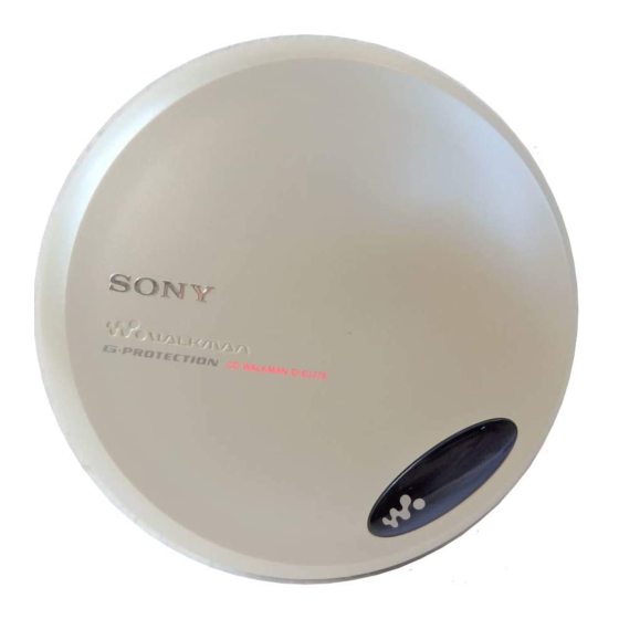
Sony D-EJ775 Service Manual
Portable cd player
Hide thumbs
Also See for D-EJ775:
- Operating instructions manual (36 pages) ,
- Operating instructions manual (20 pages)
Table of Contents
Advertisement
Quick Links
SERVICE MANUAL
Ver 1.2 2002.09
System
Compact disc digital audio system
Laser diode proper ties
Material: GaAlAs
Wavelength: λ = 780 nm
Emission duration: Continuous
Laser output: Less than 44.6 µW
(This output is the v alue measured at a distance
of 200 mm from the objecti ve lens surface on
the optical pick-up block with 7 mm aperture.)
D-A conversion
1-bit quartz time-axis control
Frequency response
+1
40 - 20 000 Hz
dB (measured by JEITA CP-
–5
307)
Output (at 4.5 V input level)
Headphones (stereo minijack)
Approx. 5 mW + Approx. 5 mW at 16 Ω
(Approx. 0.5 mW + Approx. 0.5 mW at 16 Ω)*
*For the customer s in France
Power requirements
For the area code of the model you
purchased, check the upper left side of the
bar code on the package.
• Two Son y NC-WMAA rechargeable
batteries: 2.4 V DC
• Sony NH-WM2AA rechargeable batteries:
2.4 V DC
• Two LR6 (size AA) batteries: 3 V DC
• AC power ada ptor (DC IN 4.5 V jac k):
Canadian and Taiwan models:
120 V, 60 Hz
Sony Corporation
9-873-592-03
2002I0500-1
Personal Audio Company
C 2002.09
Published by Sony Engineering Corporation
Model Name Using Similar Mechanism D-EJ955
CD Mechanism Type
Optical Pick-up Name
SPECIFICATIONS
AEP and E13 models:
220 - 230 V, 50/60 Hz
UK model: 230 - 240 V, 50 Hz
Australian model: 240 V, 50 Hz
Tourist, E33 and Korean models: 100 - 240 V,
50/60 Hz
Hong Kong model: 220 V, 50/60 Hz
Chinese model: 220 V, 50 Hz
Battery life
(approx. hours)
*
(When you use the CD player on a flat and stable
surface.)
Playing time va ries de pending on how the CD
player is used.
When using
G-PROTECTION function
on
Two NC-WMAA
12
(charged for
about 3 hours**)
NH-WM2AA
22
(charged for
about 5 hours**)
Two Sony alkaline
41
batteries LR6(SG)
(produced in Japan)
* Measured value by the standard of JEITA (Japan
Electronics and Information Te chnology
Industries Association).
** Charging time va ries depending on how the
re chargeable battery is used.
D-EJ775
Canadian Model
Australian Model
Chinese Model
Operating temperature
5°C - 35°C (41°F - 95°F)
Dimensions (w/h/d) (excluding
projecting parts and controls)
Approx. 136.0 × 19.8 × 136.0 mm
3
25
3
×
× 5
(5
⁄
⁄
⁄
8
32
8
Mass (excluding accessories)
Approx. 160 g (5.7 oz.)
Supplied accessories
For the area code of the location in which you
purchased the CD player, check the upper left side
of the bar code on the package.
AC power adaptor (1)
off
Headphones/earphones with remote control (1)
Rechargeable batteries (2)
8
Battery carrying case (1)
AC plug adaptor (1)*
17
1
Supplied with Tourist and E33 models
*
Design and specif ications ar e subject to chang e
29
without notice.
• Abbreviation
E13: 220 - 230 V AC area in E model
E33: 100 - 240 V AC area in E model
PORTABLE CD PLAYER
AEP Model
UK Model
E Model
Tourist Model
CDM-3325ES
DAX-25E
in.)
1
Advertisement
Table of Contents

Related Manuals for Sony D-EJ775


Summary of Contents for Sony D-EJ775
- Page 1 • Two Son y NC-WMAA rechargeable * Measured value by the standard of JEITA (Japan batteries: 2.4 V DC Electronics and Information Te chnology • Sony NH-WM2AA rechargeable batteries: Industries Association). 2.4 V DC ** Charging time va ries depending on how the •...
-
Page 2: Table Of Contents
SUR LES DIAGRAMMES SCHÉMATIQUES ET LA LISTE DES PIÈCES SONT CRITIQUES POUR LA SÉCURITÉ DE FONCTIONNEMENT. NE REMPLACER CES COM- POSANTS QUE PAR DES PIÈCES SONY DONT LES NUMÉROS SONT DONNÉS DANS CE MANUEL OU DANS LES SUPPLÉMENTS PUBLIÉS PAR SONY. -
Page 3: Servicing Notes
D-EJ775 SECTION 1 SERVICING NOTES MAIN BOARD IDENTIFICATION BEFORE REPLACING THE OPTICAL PICK-UP BLOCK – MAIN Board (Component Side) – Please be sure to check thoroughly the parameters as par the “Op- tical Pick-Up Block Checking Procedures” (Part No.: 9-960-027- 11) issued separately before replacing the optical pick-up block. - Page 4 D-EJ775 SERVICE MODE 2. Operation in Service Mode When the Service mode is set, the LCD on the remote commander In the Service mode, this set can check the following. displays the microcomputer version display. 1. Service Mode Setting Method To set the service mode, perform as follows.
-
Page 5: General
D-EJ775 SECTION 2 This section is extracted from instruction manual. GENERAL Getting started Remote control qg N (play)> qa Display Locating the controls (AMS/sear ch) button For details, see pages in parentheses. qs HOLD switch (rear) CD player (front) 1 . (AMS/ 5 OPEN switch search)•>... -
Page 6: Disassembly
D-EJ775 SECTION 3 DISASSEMBLY • This set can be disassembled in the order shown below. 3-1. DISASSEMBLY FLOW 3-2. LID UPPER SUB ASSY (Page 6) 3-3. PLATE (SPRING) (Page 7) 3-4. CABINET (UPPER) SUB ASSY (Page 7) 3-5. MAIN BOARD,... -
Page 7: Plate (Spring)
D-EJ775 3-3. PLATE (SPRING) 1 two screws 4 plate (spring) 3 spring (full open. A) 3 spring (full open. B) 3-4. CABINET (UPPER) SUB ASSY 1 Open battery case lid. 2 eight screws (B2) 3 claw knob (GPRO) 4 cabinet (upper) sub assy... -
Page 8: Main Board Optical Pick-Up Section (Cdm-3325Es)
D-EJ775 3-5. MAIN BOARD OPTICAL PICK-UP SECTION (CDM-3325ES) 4 connector (CN503) 5 flexible board (CN501) terminal board 3 cushion (relay), battery 4 connector (CN502) 1 screw (B) (1.4) 6 insulator 9 cushion 7 optical pick-up section (CDM-3325ES) qa main board S802 8 Remove two solders. -
Page 9: Electrical Adjustments
D-EJ775 SECTION 4 ELECTRICAL ADJUSTMENTS The CD section adjustments are done automatically in this set. EF ALIGNMENT ADJUSTMENT In case of operation check, confirm that focus bias. (for microcomputer version 052 or 057 only) Connection: oscilloscope PRECAUTIONS FOR ADJUSTMENT (DC range) 1. - Page 10 D-EJ775 Connecting and Checking/Adjustment Location: – MAIN (Conducter Side)/SUB Boards – SUB Board (MAIN Board suffix-11, -12 only) RV601 EF Alignment Adjustment (MAIN Board suffix-13 only) EF Alignment TAP802 (OPEN) Adjustment (MAIN Board suffix-11, -12 only) – MAIN Board (Conductor Side) –...
-
Page 11: Diagrams
D-EJ775 SECTION 5 DIAGRAMS 5-1. BLOCK DIAGRAM – SERVO Section – (SUFFIX-11, -12) (SUFFIX-13) RF AMP, DIGITAL SIGNAL PROCESSOR, AVDD 2V AVDD 2V RV601 DIGITAL SERVO PROCESSOR, D-RAM CONTROLLER ALIGNMENT ALIGNMENT IC601 (SUFFIX-11) IC601 (SUFFIX-12) IC601 (SUFFIX-13) DETECTOR LDACO LDACO,... -
Page 12: Block Diagram - Audio/Key Control/Power Supply Section
D-EJ775 J301 5-2. BLOCK DIAGRAM – AUDIO/KEY CONTROL/POWER SUPPLY Section – HEADPHONE AMP IC302 (SUFFIX-11) IC302 (SUFFIX-12) IC302 (SUFFIX-13) LDACO LOUT RDACO ROUT (Page 11) SYSTEM CONTROLLER IC801(2/2) (SUFFIX-11) IC801(2/2) (SUFFIX-12) IC801(2/2) (SUFFIX-13) MUTE • SIGNAL PATH AMUTE MUTE SW S808 −... -
Page 13: Note For Printed Wiring Boards And Schematic Diagrams
D-EJ775 5-3. NOTE FOR PRINTED WIRING BOARDS AND SCHEMATIC DIAGRAMS • Waveforms 6 IC601 ua (CLKDRV) 1 IC406 1 (SYNC) Note on Printed Wiring Board Note on Schematic Diagram: • X : parts extracted from the component side. • All capacitors are in µF unless otherwise noted. pF: µµF •... -
Page 14: Printed Wiring Boards - Main (Component Side) (Suffix-11)/Sub Boards
D-EJ775 5-4. PRINTED WIRING BOARDS – MAIN (Component Side) (Suffix-11)/SUB Boards – • Component Side SUB BOARD Ref. No. Location MAIN BOARD (COMPONENT SIDE) D301 D303 D304 D404 D405 D803 D406 CHARGE D408 M902 D409 S807 (SPINDLE) D410 CHARGE D411... -
Page 15: Printed Wiring Board - Main Board (Conductor Side) (Suffix-11)
D-EJ775 5-5. PRINTED WIRING BOARD – MAIN Board (Conductor Side) (Suffix-11) – • Conductor Side Ref. No. Location D302 D403 D412 D413 D801 IC401 IC402 IC405 IC406 C-10 IC601 IC801 Q401 Q402 OPTICAL PICK-UP TP514 BLOCK (OPGSW) DAX-25E IC406 TJ501... -
Page 16: Schematic Diagram - Main (1/3) (Suffix-11)/Sub Boards
D-EJ775 5-6. SCHEMATIC DIAGRAM – MAIN (1/3) (Suffix-11)/SUB Boards – • • See page 13 for Waveforms. See page 29 for IC Block Diagram. (1/3) (SUFFIX-11) M902 CN502 R626 (SPINDLE) TP508 R435 100k TAP404 R438 D408 D406 C628 TP509 L501 47µH... -
Page 17: (Suffix-11)
D-EJ775 5-7. SCHEMATIC DIAGRAM – MAIN Board (2/3) (Suffix-11) – • See page 13 for Waveform. (Page 16) (2/3) (SUFFIX-11) RESET SIGNAL GENERATOR IC405 XC61CN1402MR C415 D413 UDZS5.1B 6.3V TP415 TP414 C432 R419 TIN- TIN+ R406 PWM4 100k FIN- SIN-... -
Page 18: (Suffix-11)
D-EJ775 5-8. SCHEMATIC DIAGRAM – MAIN Board (3/3) (Suffix-11) – • • See page 13 for Waveforms. See page 29 for IC Block Diagram. (3/3) (SUFFIX-11) (Page 16) R301 R804 C804 0.022 R802 R803 R807 C818 4700p CHGMNT C102 R103... -
Page 19: Schematic Diagram - Main Board (1/3) (Suffix-12)/Sub Boards
D-EJ775 5-9. SCHEMATIC DIAGRAM – MAIN (1/3) (Suffix-12)/SUB Boards – • • See page 13 for Waveforms. See page 29 for IC Block Diagram. (1/3) (SUFFIX-12) M902 CN502 R626 (SPINDLE) TP508 R435 100k TAP404 R438 D408 D406 C628 TP509 L501 47µH... -
Page 20: Schematic Diagram - Main Board
D-EJ775 5-10. SCHEMATIC DIAGRAM – MAIN Board (2/3) (Suffix-12) – • See page 13 for Waveform. (Page 19) (2/3) (SUFFIX-12) RESET SIGNAL GENERATOR IC405 XC61CN1402MR C415 D413 UDZS5.1B 6.3V TP415 TP414 C432 R419 TIN- TIN+ R406 PWM4 100k FIN- SIN-... -
Page 21: Schematic Diagram - Main Board
D-EJ775 5-11. SCHEMATIC DIAGRAM – MAIN Board (3/3) (Suffix-12) – • • See page 13 for Waveforms. See page 29 for IC Block Diagram. (3/3) (SUFFIX-12) (Page 19) R301 R804 C804 0.022 R802 R803 R807 C818 4700p CHGMNT ATTSW ALCDET... -
Page 22: Printed Wiring Boards - Main (Component Side) (Suffix-12)/Sub Boards
D-EJ775 5-12. PRINTED WIRING BOARDS – MAIN (Component Side) (Suffix-12)/SUB Boards – • Component Side SUB BOARD Ref. No. Location MAIN BOARD (COMPONENT SIDE) D301 D303 D304 D404 D405 D803 D406 CHARGE D408 M902 D409 S807 (SPINDLE) D410 CHARGE D411... -
Page 23: Printed Wiring Board - Main Board (Conductor Side) (Suffix-12)
D-EJ775 5-13. PRINTED WIRING BOARD – MAIN Board (Conductor Side) (Suffix-12) – • Conductor Side Ref. No. Location D302 D403 D412 D413 D801 IC401 IC402 IC405 IC406 C-10 IC601 IC801 Q401 Q402 OPTICAL PICK-UP TP514 BLOCK (OPGSW) DAX-25E IC406 TJ501... -
Page 24: Printed Wiring Board - Main Board (Component Side) (Suffix-13)
D-EJ775 5-14. PRINTED WIRING BOARD – MAIN Board (Component Side) (Suffix-13) – • Component Side Ref. No. Location MAIN BOARD (COMPONENT SIDE) D301 D303 D304 D404 D803 D405 D406 CHARGE D409 D410 S807 D411 CHARGE D803 IC302 IC404 S806 IC603... -
Page 25: Printed Wiring Board -Main Board (Conductor Side) (Suffix-13)
D-EJ775 5-15. PRINTED WIRING BOARD – MAIN Board (Conductor Side) (Suffix-13) – • Conductor Side Ref. No. Location D302 D403 D412 D413 D801 IC401 IC402 IC405 IC406 C-10 IC601 IC801 Q401 Q402 OPTICAL PICK-UP TP514 BLOCK (OPGSW) DAX-25E IC406 TJ501... -
Page 26: Schematic Diagram - Main Board (1/3) (Suffix-13)
D-EJ775 5-16. SCHEMATIC DIAGRAM – MAIN Board (1/3) (Suffix-13) – • • See page 13 for Waveforms. See page 29 for IC Block Diagram. R626 (1/3) C605 100p (SUFFIX-13) C628 M902 CN502 R611 (SPINDLE) TP508 R435 100k TAP404 R612 R438... -
Page 27: Schematic Diagram - Main Board
D-EJ775 5-17. SCHEMATIC DIAGRAM – MAIN Board (2/3) (Suffix-13) – • See page 13 for Waveform. (Page 26) (2/3) (SUFFIX-13) RESET SIGNAL GENERATOR IC405 XC61CN1402MR C415 D413 UDZS5.1B 6.3V TP415 TP414 C432 R419 TIN- TIN+ R406 PWM4 100k FIN- SIN-... -
Page 28: Schematic Diagram - Main Board
D-EJ775 5-18. SCHEMATIC DIAGRAM – MAIN Board (3/3) (Suffix-13) – • • See page 13 for Waveforms. See page 29 for IC Block Diagram. (3/3) (SUFFIX-13) (Page 26) R301 R804 C804 0.022 R802 R803 R807 C818 4700p CHGMNT C102 R103... -
Page 29: Ic Block Diagrams
D-EJ775 • IC Block Diagrams IC302 TA2120FN (EL) BEEP BIAS BIAS IN B IN A BEEP BIAS OUT B OUT A RF IN PWC OUT B OUT C OUT A IC406 TB2127AFN (EL) SYNC 24 PWM XBRK 23 APWM –... -
Page 30: Ic Pin Function Description
D-EJ775 5-19. IC PIN FUNCTION DESCRIPTION • IC801 T5AJ4-3N53 (SYSTEM CONTROLLER) Pin No. Pin Name Description — Ground terminal System clock input from the DSP XOUT High frequency oscillator output terminal Not used TEST Test terminal for IC Not used VCPU —... - Page 31 D-EJ775 Pin No. Pin Name Description Terminal for doubler circuit capacitor connection to develop liquid crystal display drive voltage 64, 65 C1, C0 — Not used Wakeup control signal output to the power control (for system standby reset) XWAKEUP “L”: wakeup The stop status is reset with the falling edge of input signal...
-
Page 32: Exploded Views
D-EJ775 SECTION 6 EXPLODED VIEWS NOTE: • -XX and -X mean standardized parts, so they • Items marked “*” are not stocked since they • Abbreviation may have some difference from the original are seldom required for routine service. Some : French model one. -
Page 33: Main Section
D-EJ775 6-2. MAIN SECTION main board: suffix -11, -12 BT401 BT400 BT402 CDM-3325ES main board: suffix -11, -12 Ref. No. Part No. Description Remark Ref. No. Part No. Description Remark X-3381-716-1 CABINET (LOWER) SUB ASSY 3-242-154-01 LEAF, COPPER 3-234-106-01 INSULATOR... -
Page 34: Optical Pick-Up Section (Cdm-3325Es)
D-EJ775 Ver 1.2 6-3. OPTICAL PICK-UP SECTION (CDM-3325ES) M902 M901 The components identified by Les composants identifiés par une mark 0 or dotted line with marque 0 sont critiques pour la mark 0 are critical for safety. sécurité. Replace only with part num- Ne les remplacer que par une pièce... -
Page 35: Electrical Parts List
D-EJ775 SECTION 7 ELECTRICAL PARTS LIST MAIN (SUFFIX-11) NOTE: • Due to standardization, replacements in the • Items marked “*” are not stocked since they The components identified by parts list may be different from the parts speci- are seldom required for routine service. - Page 36 D-EJ775 MAIN (SUFFIX-11) Ref. No. Part No. Description Remark Ref. No. Part No. Description Remark C630 1-162-927-11 CERAMIC CHIP 100PF L406 1-414-392-41 INDUCTOR C634 1-162-966-11 CERAMIC CHIP 0.0022uF 10% L407 1-414-392-41 INDUCTOR C635 1-162-966-11 CERAMIC CHIP 0.0022uF 10% L415 1-414-398-11 INDUCTOR...
- Page 37 D-EJ775 MAIN (SUFFIX-11) MAIN (SUFFIX-12) Ref. No. Part No. Description Remark Ref. No. Part No. Description Remark R419 1-216-864-11 METAL CHIP 1/10W S808 1-771-248-11 SWITCH, TACTILE (SOUND) S809 1-771-248-11 SWITCH, TACTILE (VOL +) R422 1-216-864-11 METAL CHIP 1/10W S810 1-771-248-11 SWITCH, TACTILE (VOL -)
- Page 38 D-EJ775 MAIN (SUFFIX-12) Ref. No. Part No. Description Remark Ref. No. Part No. Description Remark C427 1-135-201-11 TANTALUM CHIP 10uF < CONNECTOR > C429 1-164-505-11 CERAMIC CHIP 2.2uF C431 1-162-970-11 CERAMIC CHIP 0.01uF * CN501 1-815-832-21 CONNECTOR, FFC/FPC (ZIF) 15P...
- Page 39 D-EJ775 MAIN (SUFFIX-12) Ref. No. Part No. Description Remark Ref. No. Part No. Description Remark < TRANSISTOR > R436 1-216-857-11 METAL CHIP 1/10W R437 1-216-853-11 METAL CHIP 470K 1/10W Q401 8-729-054-79 TRANSISTOR 2SB167900LSO R438 1-216-853-11 METAL CHIP 470K 1/10W Q402...
- Page 40 D-EJ775 MAIN (SUFFIX-12) MAIN (SUFFIX-13) Ref. No. Part No. Description Remark Ref. No. Part No. Description Remark < VIBRATOR > C441 1-115-156-11 CERAMIC CHIP C442 1-111-253-11 TANTALUM CHIP 100uF 6.3V X601 1-795-218-21 VIBRATOR, CERAMIC (16.934MHz) C443 1-162-968-11 CERAMIC CHIP 0.0047uF 10%...
- Page 41 D-EJ775 MAIN (SUFFIX-13) Ref. No. Part No. Description Remark Ref. No. Part No. Description Remark D404 8-719-085-43 DIODE MA2YD2300LS0 R103 1-216-833-11 METAL CHIP 1/10W D405 8-719-085-43 DIODE MA2YD2300LS0 (EXCEPT FR) D406 8-719-072-70 DIODE MA2ZD14001S0 R103 1-216-837-11 METAL CHIP 1/10W D409 8-719-069-54 DIODE UDZSTE-175.1B...
- Page 42 D-EJ775 MAIN (SUFFIX-13) Ref. No. Part No. Description Remark Ref. No. Part No. Description Remark R612 1-216-837-11 METAL CHIP 1/10W 1-685-123-11 SUB BOARD R613 1-216-837-11 METAL CHIP 1/10W ********** R614 1-216-853-11 METAL CHIP 470K 1/10W < RESISTOR > R616 1-216-817-11 METAL CHIP...
- Page 43 D-EJ775 Ref. No. Part No. Description Remark Ref. No. Part No. Description Remark 3-239-300-41 MANUAL, INSTRUCTION (POLISH) (EE) 3-239-300-51 MANUAL, INSTRUCTION (SLOVAKIAN) (EE) 3-239-300-61 MANUAL, INSTRUCTION (KOREAN) (KR) 8-954-008-91 RECEIVER,EAR MDR-E808SP/C1 SET...
-
Page 44: Revision History
D-EJ775 REVISION HISTORY Clicking the version allows you to jump to the revised page. Also, clicking the version at the upper right on the revised page allows you to jump to the next revised page. Ver. Date Description of Revision 2002.02...