Sony STR-DN850 Service Manual
Multi channel av receiver
Hide thumbs
Also See for STR-DN850:
- Service manual (106 pages) ,
- Startup manual (2 pages) ,
- Updating the software (2 pages)
Table of Contents
Advertisement
STR-DN860/DN1060
SERVICE MANUAL
Ver. 1.0 2015.02
This receiver incorporates Dolby* Digital and Pro
Logic Surround and the DTS** Digital Surround
System.
* Manufactured under license from Dolby Labo-
ratories. Dolby, Pro Logic, Surround EX, and
the double-D symbol are trademarks of Dolby
Laboratories.
** For DTS patents, see http://patents.dts.com.
Manufactured
under
license
from
DTS
Licensing Limited. DTS, DTS-HD, the
Symbol, & DTS and the Symbol together are
registered trademarks, and DTS-HD Master
Audio is a trademark of DTS, Inc. © DTS, Inc.
All Rights Reserved.
This
receiver
incorporates
High-Definition
Multimedia Interface (HDMI™) technology.
The terms HDMI and HDMI High-Definition
Multimedia Interface, and the HDMI Logo are
trademarks or registered trademarks of HDMI
Licensing LLC in the United States and other
countries.
Apple, the Apple logo, AirPlay, iPad, iPhone,
iPod, iPod classic, iPod nano, iPod touch,
and Retina are trademarks of Apple Inc.,
registered in the U.S. and other countries.
iPad Air and iPad mini are trademarks of Apple Inc.
App Store is a service mark of Apple Inc.
All other trademarks and registered trademarks
are of their respective holders. In this manual, ™
and ® marks are not specified.
"Made for iPod," "Made for iPhone," and "Made
for iPad" mean that an electronic accessory has been
designed to connect specifically to iPod, iPhone,
or iPad, respectively, and has been certified by the
developer to meet Apple performance standards.
Apple is not responsible for the operation of
this device or its compliance with safety and
regulatory standards. Please note that the use of
this accessory with iPod, iPhone, or iPad may
affect wireless performance.
Windows Media is either a registered trademark or
trademark of Microsoft Corporation in the United
States and/or other countries.
This product is protected by certain intellectual
property rights of Microsoft Corporation. Use
or distribution of such technology outside of
this product is prohibited without a license from
Microsoft or an authorized Microsoft subsidiary.
The LDAC™ name and logo is a trademark of
Sony Corporation.
"DSEE HX" is a trademark of Sony Corporation.
MPEG Layer-3 audio coding technology and
patents licensed from Fraunhofer IIS and
Thomson.
"x.v.Color
(x.v.Colour)"
and
"x.v.Color
(x.v.Colour)" logo are trademarks of Sony
Corporation.
"BRAVIA" is a trademark of Sony Corporation.
"PlayStation" is a registered trademark of Sony
Computer Entertainment Inc.
"WALKMAN" and "WALKMAN" logo are
registered trademarks of Sony Corporation.
MICROVAULT is a trademark of Sony Corpora-
tion.
9-890-661-01
Sony Corporation
2015B80-1
©
2015.02
Published by Sony EMCS (Malaysia) PG Tec
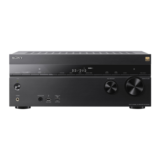
Photo: STR-DN1060
WPA™ and WPA2™ are trademarks of Wi-Fi
Alliance
®
.
The Wi-Fi CERTIFIED™ Logo is a certification
mark of Wi-Fi Alliance
®
.
MHL, Mobile High-Definition Link and the
MHL Logo are trademarks or registered trade-
marks of MHL Licensing, LLC.
®
The BLUETOOTH
word mark and logos
are registered trademarks owned by Bluetooth
SIG, Inc. and any use of such marks by Sony
Corporation is under license. Other trademarks
and trade names are those of their respective
owners.
The N Mark is a trademark or registered
trademark of NFC Forum, Inc. in the United
States and in other countries.
Android™ is a trademark of Google Inc.
Google Play™ is a trademark of Google Inc.
Notice on End User License
Agreement (EULA)
For details of the EULA for this product, see
page 14.
For details of the EULA for network services,
please refer to [License agreement] in options
menu on each network service icon.
For details of the GPL, LGPL and other software
licenses, please refer to [Software License
Information] in [System Settings] of the [Setup]
menu on this product.
This product contains software that is subject
to the GNU General Public License ("GPL") or
GNU Lesser General Public License ("LGPL").
These establish that customers have the right to
acquire, modify, and redistribute the source code
of said software in accordance with the terms of
the GPL or the LGPL.
The source code for the software used in this
product is subject to the GPL and LGPL, and is
available on the Web.
To download, please access the following:
URL:
http://oss.sony.net/Products/Linux
Please note that Sony cannot answer or respond to
any inquiries regarding the content of this source
code.
End User License Information
REAL END USER LICENSE
AGREEMENT (Taiwan models only)
1. End users are prohibited from modifying,
translating, reverse engineering, decompiling,
disassembling or using other means to discover
the software developed by Real or otherwise
replicate the functionality of the software,
except to the extent that this restriction is
expressly prohibited by applicable law.
2. Real disclaims all warranties and conditions,
express and implied, including implied
warranties or conditions of merchantability
and fitness for a particular purpose; and
effectively exclude all liability for indirect,
special, incidental and consequential damages,
including but not limited to lost profits or
replacement systems.
SPECIFICATIONS
AUDIO POWER SPECIFICATIONS
POWER OUTPUT AND TOTAL
HARMONIC DISTORTION:
(US models only)
STR-DN1060:
With 6 ohm loads, both channels driven, from
20 Hz – 20,000 Hz; rated 100 watts per channel
minimum RMS power, with no more than
0.09% total harmonic distortion from 250 milli-
watts to rated output.
STR-DN860:
With 6 ohm loads, both channels driven, from
20 Hz – 20,000 Hz; rated 95 watts per channel
minimum RMS power, with no more than
0.09% total harmonic distortion from 250 milli-
watts to rated output.
Amplifier section
STR-DN1060
US, Canadian, Australian and Taiwan models
1)
:
Minimum RMS Output Power
(6 ohms, 20 Hz – 20 kHz, THD 0.09%)
100 W + 100 W
Stereo Mode Output Power
(6 ohms, 1 kHz, THD 1%)
120 W + 120 W
Surround Mode Output Power
2)
(6 ohms, 1 kHz, THD 0.9%)
165 W per channel
STR-DN860
Minimum RMS Output Power
1)
(6 ohms, 20 Hz – 20 kHz, THD 0.09%)
95 W + 95 W
Stereo Mode Output Power
1)
(6 ohms, 1 kHz, THD 1%)
110 W + 110 W
Surround Mode Output Power
1)2)
(6 ohms, 1 kHz, THD 0.9%)
150 W per channel
1)
Measured under the following conditions:
Area
Power requirements
US, Canadian,
120 V AC, 60 Hz
Taiwan
Australian, AEP,
230 V AC, 50 Hz
UK
Reference power output for front, center,
2)
surround, surround back and front high
speakers. Depending on the sound field set-
tings and the source, there may be no sound
output.
MULTI CHANNEL AV RECEIVER
US Model
Canadian Model
AEP Model
UK Model
Australian Model
Taiwan Model
STR-DN860
Frequency response
Analog
10 Hz – 100 kHz, +0.5/–2 dB (with
sound field and equalizer bypassed)
Input
Analog
Sensitivity: 500 mV/50 kilohms
S/N
3)
: 105 dB (A, 500 mV
4)
)
Digital (Coaxial)
Impedance: 75 ohms
S/N: 100 dB (A, 20 kHz LPF)
Digital (Optical)
S/N: 100 dB (A, 20 kHz LPF)
Output (Analog)
ZONE 2
5)
Voltage: 2 V/1 kilohm
SUBWOOFER
Voltage: 2 V/1 kilohm
Equalizer
Gain levels
±10 dB, 1 dB step
INPUT SHORT (with sound field and equalizer
3)
bypassed).
Weighted network, input level.
4)
STR-DN1060 only.
5)
FM tuner section
Tuning range
US and Canadian models:
87.5 MHz – 108.0 MHz (100 kHz step)
Other models:
87.5 MHz – 108.0 MHz (50 kHz step)
Antenna (aerial)
FM wire antenna (aerial)
Antenna (aerial) terminals
75 ohms, unbalanced
Video section
Inputs/Outputs
Video:
1 Vp-p, 75 ohms
COMPONENT VIDEO*:
Y: 1 Vp-p, 75 ohms
P
: 0.7 Vp-p, 75 ohms
B
P
: 0.7 Vp-p, 75 ohms
R
80 MHz HD Standby Through
* STR-DN1060 only.
– Continued on next page –
Advertisement
Table of Contents

Related Manuals for Sony STR-DN850


Summary of Contents for Sony STR-DN850
-
Page 1: Service Manual
: 105 dB (A, 500 mV Symbol, & DTS and the Symbol together are 20 Hz – 20,000 Hz; rated 100 watts per channel SIG, Inc. and any use of such marks by Sony Digital (Coaxial) registered trademarks, and DTS-HD Master minimum RMS power, with no more than Corporation is under license. - Page 2 STR-DN860/DN1060 HDMI Video General Power requirements Input/Output (HDMI Repeater block) STR-DN1060: HDMI IN SAT/CATV (MHL) and HDMI OUT A (TV) jacks support HDCP 2.2 protocol. Area Power requirements STR-DN860: HDMI IN SAT/CATV (MHL) and HDMI TV OUT jacks support HDCP 2.2 protocol. US, Canadian, HDCP 2.2 is newly enhanced copyright protection technology that is used to protect content such as 4K movies.
- Page 3 LES DIAGRAMMES SCHÉMATIQUES ET LA LISTE DES PIÈCES SONT CRITIQUES POUR LA SÉCURITÉ DE FONC- TIONNEMENT. NE REMPLACER CES COMPOSANTS QUE PAR DES PIÈCES SONY DONT LES NUMÉROS SONT DON- NÉS DANS CE MANUEL OU DANS LES SUPPLÉMENTS PUBLIÉS PAR SONY.
-
Page 4: Table Of Contents
STR-DN860/DN1060 TABLE OF CONTENTS SERVICING NOTES 6-35. Printed Wiring Boards - PANEL Section - ..... 70 ..........6-36. Schematic Diagram - PANEL Section - ......71 6-37. Printed Wiring Board - DCDC Board - ......72 DISASSEMBLY 6-38. Schematic Diagram - DCDC Board - ......73 2-1. -
Page 5: Servicing Notes
4-547-191-1 [] Help Guide Links : DN860: Australian 4-547-191-2 [] DN860: Taiwan 4-547-191-3 [] AEP, UK Models : http://rd1.sony.net/help/ha/strdn10686/h_eu/ Except AEP, : http://rd1.sony.net/help/ha/strdn10686/h_zz/ UNLEADED SOLDER UK Models Boards requiring use of unleaded solder are printed with the lead-free mark (LF) indicating the solder contains no lead. - Page 6 STR-DN860/DN1060 NOTE OF REPLACING THE Q1550, Q1551, Q1600, NOTE OF REPLACING THE IC1906, IC1911, IC1912, Q1601, Q1650, Q1651, Q1700, Q1701, Q1750, Q1751, IC1913, IC1914 AND IC1915 ON THE DCDC BOARD Q1800, Q1801, Q1850 AND Q1851 ON THE MAIN Replacement of IC1906, IC1911, IC1912, IC1913, IC1914 and BOARD IC1915 on the DCDC Board used in this unit required to unsolder Replacement of Q1550, Q1551, Q1600, Q1601, Q1650, Q1651,...
-
Page 7: Resetting Sound Fields To The Default Settings
Be sure to use the buttons on the receiver restore the receiver to the factory default to perform this operation. persists, consult your nearest Sony dealer. settings by the following procedure. This 1. Turn off the receiver. procedure can also be used to initialize 2. - Page 8 STR-DN860/DN1060 NOTE OF REPLACING MB-1409 BOARD OR WLAN/ (Screen 3) BT COMBO CARD Diag When the MB-1409 board or WLAN/BT COMBO card are Category: Bluetooth Device Test replaced, please execute the below service mode. [1] Bluetooth Enable Procedure: [2] Bluetooth Disable [3] Write Bluetooth device address to Registry While pressing [DISPLAY] button, press and release the [MUSIC], [4] Bluetooth Inquiry Test...
-
Page 9: Disassembly
STR-DN860/DN1060 SECTION 2 DISASSEMBLY • This set can be disassembled in the order shown below. 2-1. DISASSEMBLY FLOW 2-2. CASE (ENTRY) (DN860) 2-3. CASE (STEPUP) (DN1060) (Page 10) (Page 10) 2-5. CARD WLAN/BT COMBO 2-4. CARD WLAN/BT COMBO (DN1060) (DN860) (Page 12) (Page 11) 2-7. -
Page 10: Case (Entry) (Dn860)
STR-DN860/DN1060 Note: Follow the disassembly procedure in the numerical order given. 2-2. CASE (ENTRY) (DN860) 3 three screws (+BVTP 3 1 three screws (B-TYPE 4 5 case (entry) 2 three screws (B-TYPE 4 2-3. CASE (STEPUP) (DN1060) 3 four screws (+BVTP 3 1 three screws (B-TYPE 4... -
Page 11: Card Wlan/Bt Combo (Dn860)
STR-DN860/DN1060 2-4. CARD WLAN/BT COMBO (DN860) cushion (R) rear side cable tie MB-1409 board clamp DCDC board Note: Process so that lead wire does not contact CN301 and W1990 4 cushion (R) 3 cushion (R) 0 one screw (+BVTP 3 1 Wire is removed rear side from the clamp. -
Page 12: Card Wlan/Bt Combo (Dn1060)
STR-DN860/DN1060 2-5. CARD WLAN/BT COMBO (DN1060) cushion (R) rear side MB-1409 board DCDC board Note: Process so that lead wire does not contact CN301 and W1990 8 one screw (+BVTP 3 2 cushion (R) rear side cushion (R) 9 card WLAN/BT combo cushion (R) 1 CN502 (5P) 7 bracket,... -
Page 13: Mb-1409 Board (Dn860)
STR-DN860/DN1060 2-6. MB-1409 BOARD (DN860) qa one screw qh heat sink (HDMI-B) (+BVTP 3 qg heat sink (HDMI-A) qf four screws (+BVTP 3 qa two screws qd bracket, HDMI (+BVTP 3 (N86) qa three screws (+BVTP 3 pin, lead pin, lead and cable tie qs clamp qs clamp qk MB-1409 board... -
Page 14: Mb-1409 Board (Dn1060)
STR-DN860/DN1060 2-7. MB-1409 BOARD (DN1060) qd one screws wf heat sink (HDMI-B) (+BVTP 3 wd heat sink (HDMI-A) ws four screws (+BVTP 3 qd one screw (+BVTP 3 qf Cut the cable tie qg clamp qh bracket, HDMI (N86) qd one screw (+BVTP 3 wg sheet, radiation qd one screw (+BVTP 3 qg clamp... -
Page 15: Front Panel Section
STR-DN860/DN1060 2-8. FRONT PANEL SECTION (DN860) POWERKEY MAIN board board (DN1060) rear side cushion (R) cable tie MB-1409 board pin, lead rear side (DN1060) MAIN board pin, lead SUPPORT board rear side (DN1060) 2 Wire is removed from the pin, lead. (DN1060) 6 one screw 4 CN1391... -
Page 16: Back Panel Section (Dn860)
STR-DN860/DN1060 2-9. BACK PANEL SECTION (DN860) 6 three screws 5 five screws (+BVTP 3 (+BVTP 3 2 Cut the cable tie 7 back panel section 6 eight screws (+BVTP 3 3 CN1905 (4P) 1 CNP901 (3P) 4 CN1907 (2P) DCDC board clamp, sleeve ferrite cushion (R) -
Page 17: Back Panel Section (Dn1060)
STR-DN860/DN1060 2-10. BACK PANEL SECTION (DN1060) 4 eight screws 4 seven screws (+BVTP 3 (+BVTP 3 6 back panel section 5 four screws (+BVTP 3 (US, CND) four screws (BV/RING) (AEP, UK, AUS) 2 CN1905 (4P) 1 CNP901 (3P) 3 CN1907 (2P) DCDC board clamp, sleeve ferrite... -
Page 18: Standby Board, Main Board Section
STR-DN860/DN1060 2-11. STANDBY BOARD, MAIN BOARD SECTION 2 four screws (+BVTP 3 7 two screws (+BVTP 3 3 STANDBY board 4 Wire is removed from the pin, lead. 7 two screws (+BVTP 3 MAIN board 1 CNP902 (4P) rear side 9 MAIN BOARD section pin, lead... -
Page 19: Main Board
STR-DN860/DN1060 2-12. MAIN BOARD Note : This illustration sees the MAIN board from back side. 4 USB INSULATION board 2 INSULATION board 3 one screw (+BVTP 3 (DN1060) 1 one screw 5 two screws (+BVTP 3 (+BVTP 3 (DN1060) 6 SUPPORT 8 bracket, support beam board 7 one screw... -
Page 20: Test Mode
STR-DN860/DN1060 SECTION 3 TEST MODE VACUUM FLUORESCENT DISPLAY TEST MODE SWAP ALL MODE All fl uorescent segments are tested. The signal will be swap to all channels so that all speakers will When this test is activated, all segments light on at the same time, have sound output. - Page 21 STR-DN860/DN1060 HISTORY MODE MHL VBUS MODE The state that the set is used is memorized. This mode is to display the MHL VBUS status. Procedure: Procedure: 1. While pressing [SPEAKERS] and [DISPLAY] buttons 1. Press the [?/1] button to turn on the main power. simultaneously, press the [ ] button to turn on the power 2.
- Page 22 STR-DN860/DN1060 SVC SERVICE MODE Note: The operation in this mode must use a remote commander and TV monitor. Setting method of the SVC service mode: 1. Connect this unit with TV monitor. 2. Press the [ ] button to turn the power on. 3.
-
Page 23: Menu Tree
STR-DN860/DN1060 2. Menu Tree Service Device Test Service [1] Dia [1] Dia [ ] Lo [ ] Lo [3] Factory Initialize [3] Factory Initialize [4] Network [4] Network [5] Version Up [5] Version Up Video Test [6] System Information [6] System Information Not used [8] Drive udio Test... - Page 24 STR-DN860/DN1060 3. Service Mode Menu (Top Menu) 4. Diag (Device Test) This is the top menu of service mode. This screen is used to test devices mounted on the board. Each function is accessed from this screen. Operation: Screen 1: Selects the test category Moves to Diag screen Operation: Moves to Log screen...
- Page 25 STR-DN860/DN1060 5. Diag (Wireless LAN Test) 6. Diag (MIC Input Test) This screen performs wireless LAN/Miracast test. This screen performs MIC input test. Note: Not used for the servicing. Screen 1: Selects Wireless LAN Test Category 7. Diag (HDMI Input Test) Operation: This screen performs HDMI input test.
- Page 26 STR-DN860/DN1060 10. Log: Error Log (Output of each Log) (Screen 1) This screen displays the contents of each log. Diag Note: Do not refer to the displayed date. Category: Bluetooth Device Test Screen 1: Selects log Operation: Diag [1]/[ ] Moves to the Error Log output screen Category: Bluetooth Device Test [RETURN] Returns to the top menu of the service mode...
- Page 27 STR-DN860/DN1060 11. Factory Initialize (Factory Settings) Contents List: Return all of the unit setting to their factory defaults. Main LSIname Operation: Model 1. Press the [ ] button to turn the power on. Destination 2. While pressing [DISPLAY] button, press and release the Sequence Number [MUSIC], [A.F.D/2CH], [MOVIE] button in order, the message “SERVICE IN”...
-
Page 28: Fm Tuner Check
STR-DN860/DN1060 SECTION 4 FM TUNER CHECK FM AUTO STOP CHECK signal generator Procedure: 1. Turn on the set. 2. Input the following signal from signal generator to FM antenna input directly. Carrier frequency : A = 87.5 MHz, B = 98 MHz, C = 108 MHz Deviation : 75 kHz Modulation... -
Page 29: Troubleshooting
STR-DN860/DN1060 SECTION 5 TROUBLESHOOTING... - Page 30 STR-DN860/DN1060...
- Page 31 STR-DN860/DN1060...
- Page 32 STR-DN860/DN1060...
- Page 33 STR-DN860/DN1060...
-
Page 34: Diagrams
STR-DN860/DN1060 SECTION 6 DIAGRAMS • Circuit Boards Location STANDBY board DCDC board MB-1409 board NFC-ICON board card WLAN/BT COMBO RC-S730 (WW) GND BRACKET board POWERKEY board HP board FRONTJACK board MAIN board FRONT HDMI board (DN1060) DISPLAY board... -
Page 35: Block Diagram - Analog Audio Section
STR-DN860/DN1060 6-1. BLOCK DIAGRAM – ANALOG AUDIO Section – DIR FUNCTION SELECT J1403: DN860 IC1414 J1402: DN1060 INL7 AUDIO TV IN R-ch R-ch INR7 >001B ADCL L-IN DIGITAL SECTION J1401 (1/2) R-ch ADCR INL4 (Page 36) AUDIO SA-CD/CD IN R-ch R-ch INR4 AUDIO... -
Page 36: Block Diagram - Digital Section (1/2)
STR-DN860/DN1060 6-2. BLOCK DIAGRAM – DIGITAL Section (1/2) – >001B ANALOG AUDIO L-IN ADINL SECTION R-ch ADINR (Page 35) STEREO D/A CONVERTER IC6000 IC6501 XOUT X6000 VOUT1 L/R_IN SBL/SBR_OUT DATA4 24.576MHz VOUT2 R-CH DATAOUT DIR_IN SL/SR_OUT DATA3 MPOUT4 A/D_2CH WAVE SHAPER VOUT7 IC6001 C/SW1_OUT... -
Page 37: Block Diagram - Digital Section (2/2)
STR-DN860/DN1060 6-3. BLOCK DIAGRAM – DIGITAL Section (2/2) – D/A DIGITAL SIGNAL PROCESSORS HDMI RECEIVER HDMI SWITCH HDMI TRANSCEIVER AND CONTROLLERS IC5010 IC3821 IC3700 (1/2) IC7100 CN5012 CN3502 DATA2+ DATA2+ 48 D2+_1 27 R1X2+ T0X2+ RX2P TX2P D2+_SINK (DN1060) DATA2– DATA2–... -
Page 38: Block Diagram - Amp Section
STR-DN860/DN1060 6-4. BLOCK DIAGRAM – AMP Section – J1101 POWER AMP PHONES BOOSTER Q1720 Q1700 CURRENT CURRENT Q1722 LIMITER RELAY DETECT DETECT D1700 Q1702, Q1703 DRIVER Q1724 Q1704 Q1705 Q1375 BOOSTER RY1390 Q1725 TB1501 (1/2) Q1701 BOOSTER FRONT A Q1770 Q1750 Q1772 CURRENT... -
Page 39: Block Diagram - Analog Video/Usb Section
STR-DN860/DN1060 6-5. BLOCK DIAGRAM – ANALOG VIDEO/USB Section – DN1060 VIDEO AMPLIFIER IC1240 J1201 (1/2) VOUT3 VOUT2 MONITOR VOUT1 COMPONENT VIDEO VIN3 SAT/CATV V_COM_MUTE 7 POWER SAVE VIN2 (ASSIGNABLE) IN VIN1 >005B DIGITAL J1202: DN860 VIDEO SWITCH DN1060 J1201 (2/2): DN1060 DN860 IC1232 SECTION (1/2) -
Page 40: Block Diagram - Digital Video Section
STR-DN860/DN1060 6-6. BLOCK DIAGRAM – DIGITAL VIDEO Section – HDMI RECEIVER BD DECODER IC5001 IC3700 (2/2) IC101 (3/3) CN5001 EEPROM DATA2+ RX2P TXCN 35 R2X2+ R4X2+ IC110 DATA2– RX2N TXCP R2X2- R4X2- DATA1+ RX1P TX0N R2X1+ R4X1+ DATA1– RX1N TX0P R2X1- R4X1- DATA0+... -
Page 41: Block Diagram - Display/Power Section
STR-DN860/DN1060 6-7. BLOCK DIAGRAM – DISPLAY/POWER Section – VACUUM FLOURESCENT RELAY DRIVER BRIDGEABLE_RY DISPLAY Q920 ND1100 RY920 RECT LED DRIVER PURE_DIRECT_LED (PURE DIRECT) D921 Q1102 D1108 F912 (VCC) AUDIO AMP 51 FL_LAT SECTION F913 LED DRIVER 60 FL_CLK (VCC) FLASH_CLK/PWR_LED Q1110 59 FL_DATA (ON/STBY) - Page 42 STR-DN860/DN1060 THIS NOTE IS COMMON FOR PRINTED WIRING BOARDS AND SCHEMATIC DIAGRAMS. • Waveforms (In addition to this, the necessary note is printed in each block.) – MB-1409 Board – For Printed Wiring Boards. For Schematic Diagrams. Note: Note: IC401 5 (2Y) IC6002 5 (LRCKIN) IC6501 ug (BCLK_IN) •...
-
Page 43: Printed Wiring Board - Mb-1409 Board (Component Side)
STR-DN860/DN1060 6-8. PRINTED WIRING BOARD – MB-1409 Board (Component Side) – • See page 34 for Circuit Boards Location. • : Uses unleaded solder. MB-1409 BOARD FRONT HDMI (COMPONENT SIDE) BOARD (DN1060) J6000 DN860 CN4040 COAXIAL DN1060 SA-CD/CD (ASSIGNABLE) IN (Page 76) HDMI 4K IR REMOTE... -
Page 44: Printed Wiring Board - Mb-1409 Board (Conductor Side)
STR-DN860/DN1060 6-9. PRINTED WIRING BOARD – MB-1409 Board (Conductor Side) – • See page 34 for Circuit Boards Location. • : Uses unleaded solder. MB-1409 BOARD (CONDUCTOR SIDE) DN860 DN1060 R5021 R3537 R3532 C5002 FB5002 R3576 C5020 JL3822 IC3510 JL6000 Q3005 C5006 C5278... -
Page 45: Schematic Diagram - Mb-1409 Board (1/18)
STR-DN860/DN1060 6-10. SCHEMATIC DIAGRAM – MB-1409 Board (1/18) – • See page 91 for IC Pin Function Descriptions. IC101 (1/15) MB-1409 BOARD (1/18) CXD90028GB-B (EXCEPT TW) IC101 CXD90028GB-C (TW) C101 BD DECODER DDR3_ACH 0.1u AG14 D0DQ0 JL2101 DDRVCCIO1 RDQ0 D0DQ1 IC102 IC103 AF15... -
Page 46: Schematic Diagram - Mb-1409 Board (2/18)
STR-DN860/DN1060 6-11. SCHEMATIC DIAGRAM – MB-1409 Board (2/18) – • See page 79 for IC Block Diagrams. • See page 91 for IC Pin Function Descriptions. IC101 (5/15) MB-1409 BOARD (2/18) CXD90028GB-B (EXCEPT TW) MTK_3.3V IC2001 CXD90028GB-C (TW) S34ML04G200TFI003 IC101 MTK_1.2V IC2001 IC101 (6/15) -
Page 47: Schematic Diagram - Mb-1409 Board (3/18)
STR-DN860/DN1060 6-12. SCHEMATIC DIAGRAM – MB-1409 Board (3/18) – MB-1409 BOARD (3/18) CN301 C386 100p C387 0.0022u CL303 C391 C392 C390 AC CUT 0.1u C389 470p 0.0022u 0.0022u CL304 POWER-RY CL305 STANDBY +4.5V CL306 >006S DADCDC 4.5V CL307 USBDCDC_6.2V USBDCDC_6.2V DCDC BOARD JL313 CL308... -
Page 48: Schematic Diagram - Mb-1409 Board (4/18)
STR-DN860/DN1060 6-13. SCHEMATIC DIAGRAM – MB-1409 Board (4/18) – • See page 42 for Waveforms. • See page 91 for IC Pin Function Descriptions. MB-1409 BOARD (4/18) R430 R431 IC101 (8/15) CXD90028GB-B (EXCEPT TW) CXD90028GB-C (TW) IC101 MTKSTB_3.3V CN401 BD DECODER R465 2.2k RB401... -
Page 49: Schematic Diagram - Mb-1409 Board (5/18)
STR-DN860/DN1060 6-14. SCHEMATIC DIAGRAM – MB-1409 Board (5/18) – • See page 79 for IC Block Diagrams. • See page 91 for IC Pin Function Descriptions. MB-1409 BOARD (5/18) IC503 TPS2553DBVR IC503 FRONT USB VBUS USB_5.2V C531 R530 ILIM USB_PCONT FAULT R532 IC504... -
Page 50: Schematic Diagram - Mb-1409 Board (6/18)
STR-DN860/DN1060 6-15. SCHEMATIC DIAGRAM – MB-1409 Board (6/18) – • See page 91 for IC Pin Function Descriptions. IC101 (13/15) MB-1409 BOARD (6/18) CXD90028GB-B (EXCEPT TW) CXD90028GB-C (TW) MTK_3.3V IC101 R449 >001S C421 MTK_1.2V BD DECODER IC101 (14/15) MB-1409 BOARD CXD90028GB-B (EXCEPT TW) 1.2V_DDR... -
Page 51: Schematic Diagram - Mb-1409 Board (7/18)
STR-DN860/DN1060 6-16. SCHEMATIC DIAGRAM – MB-1409 Board (7/18) – • See page 79 for IC Block Diagrams. MB-1409 BOARD (7/18) >018S MB-1409 BOARD IN3_5VP (10/18) IN3_HPD (Page 54) R5050 IN3_SDA R5051 IN3_SCL R5385 Q5006 LTA043EUBFS8TL HPD SWITCH R5289 JL5008 C5038 R5026 R5025 2.2u... -
Page 52: Schematic Diagram - Mb-1409 Board (8/18)
STR-DN860/DN1060 6-17. SCHEMATIC DIAGRAM – MB-1409 Board (8/18) – • See page 79 for IC Block Diagrams. MB-1409 BOARD (8/18) >022S MB-1409 BOARD (11/18) (Page 55) >021S JL5071 MB-1409 BOARD C5138 R5168 R5166 (15/18) 2.2u IC5009 (Page 59) R5190 W25X20CLSNIG C5139 HOLD DO(IO1) -
Page 53: Schematic Diagram - Mb-1409 Board (9/18)
STR-DN860/DN1060 6-18. SCHEMATIC DIAGRAM – MB-1409 Board (9/18) – • See page 79 for IC Block Diagrams. >023S MB-1409 BOARD (9/18) MB-1409 BOARD (8/18), (11/18) (Page 52), (Page 55) DN1060 CN3500 R3500 >026S R3501 INF_5VP FRONT HDMI BOARD R3502 R3503 INF_HPD (DN1060) R3508... -
Page 54: Schematic Diagram - Mb-1409 Board (10/18)
STR-DN860/DN1060 6-19. SCHEMATIC DIAGRAM – MB-1409 Board (10/18) – • See page 42 for Waveforms. • See page 91 for IC Pin Function Descriptions. >030S MB-1409 BOARD (10/18) >028S MB-1409 BOARD (11/18) (Page 55) MB-1409 BOARD (9/18) >031S (Page 53) MB-1409 BOARD (15/18) (Page 59) C3706... -
Page 55: Schematic Diagram - Mb-1409 Board (11/18)
STR-DN860/DN1060 6-20. SCHEMATIC DIAGRAM – MB-1409 Board (11/18) – • See page 42 for Waveforms. • See page 79 for IC Block Diagrams. • See page 91 for IC Pin Function Descriptions. >037S MB-1409 BOARD (11/18) >022S MB-1409 BOARD (18/18) MB-1409 BOARD (8/18) (Page 62) (Page 52) -
Page 56: Schematic Diagram - Mb-1409 Board (12/18)
STR-DN860/DN1060 6-21. SCHEMATIC DIAGRAM – MB-1409 Board (12/18) – • See page 42 for Waveforms. • See page 79 for IC Block Diagrams. J6000 COAXIAL SA-CD/CD (ASSIGNABLE) IN MB-1409 BOARD (12/18) >038S DN1060 MB-1409 BOARD (11/18) JW6002 JW6000 (Page 55) >042S MB-1409 BOARD JL6000... -
Page 57: Schematic Diagram - Mb-1409 Board (13/18)
STR-DN860/DN1060 6-22. SCHEMATIC DIAGRAM – MB-1409 Board (13/18) – • See page 79 for IC Block Diagrams. MB-1409 BOARD (13/18) >047S MB-1409 BOARD >017S (14/18) MB-1409 BOARD (6/18) (Page 58) MTK_MCLK FB6011 CL6000 (Page 50) IC6007 SRC4190IDBR IC6007 HDMI_MUTE IC6003 R6064 TC7WH157FK LGRP... -
Page 58: Schematic Diagram - Mb-1409 Board (14/18)
STR-DN860/DN1060 6-23. SCHEMATIC DIAGRAM – MB-1409 Board (14/18) – • See page 42 for Waveforms. • See page 79 for IC Block Diagrams. • See page 91 for IC Pin Function Descriptions. MB-1409 BOARD (14/18) DA_3.3V >039S MB-1409 BOARD (11/18) X6500 25MHz (Page 55) -
Page 59: Schematic Diagram - Mb-1409 Board (15/18)
STR-DN860/DN1060 6-24. SCHEMATIC DIAGRAM – MB-1409 Board (15/18) – • See page 91 for IC Pin Function Descriptions. MB-1409 BOARD (15/18) C7156 C7154 0.15u 0.15u R7156 R7154 R7169 4.7k R7157 R7155 R7167 4.7k R7159 4.7k C7155 C7157 R7160 4.7k 0.012u 0.012u R7162 4.7k... -
Page 60: Schematic Diagram - Mb-1409 Board (16/18)
STR-DN860/DN1060 6-25. SCHEMATIC DIAGRAM – MB-1409 Board (16/18) – • See page 91 for IC Pin Function Descriptions. MB-1409 BOARD (16/18) >048S MB-1409 BOARD (15/18) (Page 59) FB7200 C7200 C7494 C7495 C7201 0.1u C7202 0.1u FB7207 C7203 0.1u C7204 0.1u AA10 R7252 DDR_DQ[31]... -
Page 61: Schematic Diagram - Mb-1409 Board (17/18)
STR-DN860/DN1060 6-26. SCHEMATIC DIAGRAM – MB-1409 Board (17/18) – • See page 79 for IC Block Diagrams. • See page 91 for IC Pin Function Descriptions. MB-1409 BOARD (17/18) >034S MB-1409 BOARD (10/18) (13/18) (Page 54), (Page 57) >035S MB-1409 BOARD (11/18) R7512 (Page 55) >049S... -
Page 62: Schematic Diagram - Mb-1409 Board (18/18)
STR-DN860/DN1060 6-27. SCHEMATIC DIAGRAM – MB-1409 Board (18/18) – • See page 79 for IC Block Diagrams. >043S MB-1409 BOARD (18/18) MB-1409 BOARD (12/18) (Page 56) >037S MB-1409 BOARD (11/18) (Page 55) CN8001 OPTICAL_TV CL8000 OPTICAL_TV CL8001 DGND OPTICAL_SAT CL8002 OPTICAL_SAT DN1060 CL8003... -
Page 63: Printed Wiring Board - Main Board (Component Side)
STR-DN860/DN1060 6-28. PRINTED WIRING BOARD – MAIN Board (Component Side) – • See page 34 for Circuit Boards Location. • : Uses unleaded solder. MAIN BOARD (COMPONENT SIDE) DN860 DN1060 J1201 J1401 J1202 COMPONENT VIDEO TB1501 TB1502 TB1503 J1402 SURROUND BACK/ BI-AMP/ MONITOR SAT/CATV SURROUND/ZONE 3... -
Page 64: Printed Wiring Board - Main Board (Conductor Side)
STR-DN860/DN1060 6-29. PRINTED WIRING BOARD – MAIN Board (Conductor Side) – • See page 34 for Circuit Boards Location. • : Uses unleaded solder. MAIN BOARD (CONDUCTOR SIDE) DN860 DN1060 R1218 JL1262 C1402 CL1339 R1217 C1401 CL1517 JL1260 CL1224 CL1231 CC1001 CL1248 CL1200... -
Page 65: Schematic Diagram - Main Board (1/5)
STR-DN860/DN1060 6-30. SCHEMATIC DIAGRAM – MAIN Board (1/5) – >054S MAIN MAIN BOARD BOARD (4/5) (1/5) (Page 68) >055S C1548 R1544 0.1u MAIN BOARD CL1865 (2/5) C1545 47u 25V R1550 R1850 R1800 R1650 R1750 R1600 R1700 L1600 L1550 L1850 L1800 L1650 L1750 L1700... -
Page 66: Schematic Diagram - Main Board (2/5)
STR-DN860/DN1060 6-31. SCHEMATIC DIAGRAM – MAIN Board (2/5) – MAIN BOARD (2/5) DN1060: AEP, UK, AUS R1394 R1396 R1398 FR_OUT FL_OUT R1399 >055S R1395 R1397 Q1321 Q1320 2PD601ART MAIN BOARD PROTECTOR MSB92T1G PROTECTOR (1/5) R1390 R1392 (Page 65) R1320 C1320 R1391 R1393 220u 10V... -
Page 67: Schematic Diagram - Main Board (3/5)
STR-DN860/DN1060 6-32. SCHEMATIC DIAGRAM – MAIN Board (3/5) – • See page 79 for IC Block Diagrams. >060S >057S MAIN BOARD MAIN BOARD (2/5) (1/5) (Page 66) (Page 65) 15 16 MAIN BOARD (3/5) >066S MAIN BOARD (4/5) (Page 68) CN1392 C1487 0.1u... -
Page 68: Schematic Diagram - Main Board (4/5)
STR-DN860/DN1060 6-33. SCHEMATIC DIAGRAM – MAIN Board (4/5) – >054S >063S >058S MAIN BOARD MAIN BOARD MAIN BOARD (1/5) (2/5) (1/5) (Page 65) (Page 66) (Page 65) 33 34 MAIN BOARD (4/5) >067S MAIN BOARD (3/5) (Page 67) R1360 R1355 R1367 R1350 2.2k... -
Page 69: Schematic Diagram - Main Board (5/5)
STR-DN860/DN1060 6-34. SCHEMATIC DIAGRAM – MAIN Board (5/5) – • See page 79 for IC Block Diagrams. MAIN BOARD (5/5) >068S C1202 MAIN BOARD (4/5) C1206 (Page 68) TUNER_GND IC1237 MM1839A33NRE IC1237 C1204 L1200 +3.3V REG. 22nH X1200 12MHz 0.1 0.2 3.3 C1221 TUNER_CE R1204... -
Page 70: Printed Wiring Boards - Panel Section
STR-DN860/DN1060 6-35. PRINTED WIRING BOARDS – PANEL Section – • See page 34 for Circuit Boards Location. • : Uses unleaded solder. >003P DISPLAY BOARD T1100 MB-1409 BOARD DN860 CN3004 DN1060 (Page 43) R1158 ND1100 LP1002 VACUUM FLOURESCENT DISPLAY CL1115 Q1101 CN1102 R1172... -
Page 71: Schematic Diagram - Panel Section
STR-DN860/DN1060 6-36. SCHEMATIC DIAGRAM – PANEL Section – DISPLAY BOARD CN1102 CL1110 27 FL_GND CL1115 26 FL_5V CL1111 25 FL_GND 24 FL_GND CL1112 23 DGND/ZONE POWER CL1113 22 FL_DATA CL1114 21 AD2 CL1147 20 FL_CLK CL1117 19 FL_BK CL1116 18 FL_STB/LATCH >041S CL1118 17 DCAC_SIGNAL... -
Page 72: Printed Wiring Board - Dcdc Board
STR-DN860/DN1060 6-37. PRINTED WIRING BOARD – DCDC Board – • See page 34 for Circuit Boards Location. • : Uses unleaded solder. DCDC BOARD (COMPONENT SIDE) MB-1409 STANDBY POWER BOARD BOARD >001P >014P TRANSFORMER CN301 CN940 >015P (MAIN) (Page 43) (Page 74) T901 (Page 74) -
Page 73: Schematic Diagram - Dcdc Board
STR-DN860/DN1060 6-38. SCHEMATIC DIAGRAM – DCDC Board – • See page 79 for IC Block Diagrams. DCDC BOARD F940 D1924 5A 250V >072S D5SBA60-F D906 L1931 SA10QA04 CN1907 CL1906 2.2uH CL1947 POWER CL1949 C1950 CL1904 0.22u TRANSFORMER C1901 R3 Green C1943 R1932 6800u... -
Page 74: Printed Wiring Board - Standby Board
STR-DN860/DN1060 6-39. PRINTED WIRING BOARD – STANDBY Board – • See page 34 for Circuit Boards Location. • : Uses unleaded solder. STANDBY BOARD STANDBY BOARD (COMPONENT SIDE) (CONDUCTOR SIDE) T902 POWER TRANSFORMER (SUB) C961 C960 >014P C962 C963 D905 A/K A DCDC CL906... -
Page 75: Schematic Diagram - Standby Board
STR-DN860/DN1060 6-40. SCHEMATIC DIAGRAM – STANDBY Board – STANDBY BOARD >069S CN940 MAIN BOARD (4/5) >073S CNP920 PWR RY F901 T3.15AL 250V (Page 68) AC CUT D992 D994 DCDC BOARD R984 (AEP, UK, AUS) RB521SM-30GJT2R CES521 CL904 STBY GND T6.3AL 250V CN1905 (TW) 8A 125V... -
Page 76: Printed Wiring Board - Frontjack Board
STR-DN860/DN1060 6-41. PRINTED WIRING BOARD – FRONTJACK Board – 6-43. PRINTED WIRING BOARD – FRONT HDMI Board (DN1060) – • • • See page 34 for Circuit Boards Location. : Uses unleaded solder. • See page 34 for Circuit Boards Location. : Uses unleaded solder. -
Page 77: Schematic Diagram - Front Hdmi Board (Dn1060)
STR-DN860/DN1060 6-44. SCHEMATIC DIAGRAM – FRONT HDMI Board (DN1060) – 6-45. PRINTED WIRING BOARD – POWERKEY Board – • See page 79 for IC Block Diagrams. • • See page 34 for Circuit Boards Location. : Uses unleaded solder. POWERKEY BOARD (VIDEO 2 IN) HDMI... -
Page 78: Printed Wiring Board - Hp Board
STR-DN860/DN1060 6-47. PRINTED WIRING BOARD – HP Board – 6-48. SCHEMATIC DIAGRAM – HP Board – • • See page 34 for Circuit Boards Location. : Uses unleaded solder. HP BOARD HP BOARD CN1107 J1101 >061S PHONES CL1185 HP_DETECT MAIN BOARD CL1186 (2/5) HP_R... -
Page 79: Ic Block Diagrams
STR-DN860/DN1060 • IC Block Diagrams IC1911 TPS54394 PWPR (DCDC BOARD) VIN1 VBST1 PGND1 -16% – – Comp +16% VREG5 PGND -32% Control logic – Xcon Ref1 PGND1 Comp – Ref_OCL PGND1 – – PGND OCP1 EN Logic Logic VIN1 VFB1 CH1 Min-off timer 5VREG CH2 Min-off timer... - Page 80 STR-DN860/DN1060 IC1232 NJM41050V (TE2) (MAIN BOARD (5/5)) CLAMP VIN1 SREFV ADVANCED 12 VSAG CORRECTION CLAMP 11 SREFV VIN2 10 VCC 9 GND DRIVER 6.75MHz CLAMP LOW-PASS 8 VOUT FILTER – VIN3 IC1236 RN5B701-0001 (MAIN BOARD (5/5)) (US and Canadian models) IISD IISD Digital Signal Processing...
- Page 81 STR-DN860/DN1060 IC1237 MM1839A33NRE (MAIN BOARD (5/5)) CONT 1 BIAS CURRENT LIMIT – REGULATOR VOUT THERMAL VOLTAGE SHUTDOWN REFERENCE GND 2 NC 3 IC1240 NJM2580V (TE1) (MAIN BOARD (5/5)) (DN1060) 14 V+1 75 ohm VIN1 13 VOUT1 DRIVER GND1 12 V+2 BIAS 75 ohm VIN2...
- Page 82 STR-DN860/DN1060 IC503 TPS2553DBVR (MB-1409 BOARD (5/18)) IC3500 TPS2553DBVR (MB-1409 BOARD (9/18)) (DN1060) IC5021 TPS2553DBVR (MB-1409 BOARD (7/18)) REVERSE VOLTAGE COMPARATOR – CURRENT IN 1 6 OUT SENSE 4-ms DEGLITCH CHARGE GND 2 PUMP CURRENT EN 3 DRIVER LIMIT UNDERVOLTAGE 5 ILLM LOCKOUT 4 FAULT 8-ms...
- Page 83 STR-DN860/DN1060 IC3000 BR24T64FJ-WE2 (MB-1409 BOARD (11/18)) 1Kbit~1024Kbit EEPROM array 8bit 7bit 13bit Address Word Data 8bit 14bit A1 2 9bit 15bit decoder address register register 10bit 16bit 11bit 17bit 12bit START STOP A2 3 Control circuit High voltage Power source GND 4 generating circuit voltage detection...
- Page 84 STR-DN860/DN1060 IC3821 TMDS261BPAGR (MB-1409 BOARD (9/18)) 45 44 42 41 39 38 37 36 35 34 33 LOCAL I2C CONTROL 32 S1/SCL LOGIC 31 HPD_SINK CLOCK DETECT CLOCK DETECT TMDS RX TMDS RX W/AEQ TMDS RX W/AEQ 30 SDA_SINK TMDS RX W/AEQ 29 SCL_SINK HPD2 28 GND...
- Page 85 STR-DN860/DN1060 IC5000 W25X20CLSNIG (MB-1409 BOARD (7/8)) IC5009 W25X20CLSNIG (MB-1409 BOARD (8/18)) Write Control Logic HOLD Status Register High Voltage Generators Page Address Latch / Counter Command and Column Decode Control Logic and 256 Byte Page Buffer Data Byte Address Latch / Counter IC5001 SII9679CNUC (MB-1409 BOARD (7/18)) VDD33OUT HSIC_VDD33...
- Page 86 STR-DN860/DN1060 IC5010 SII9678CNUC (MB-1409 BOARD (8/18)) VDD33OUT HSIC_VDD33 VDD5V_IN VDD12OUT RPWR5V HSIC_GND Regulator RX_HPD HSIC_STB Local I COC_GND Slave Logic HSIC_DAT AVDD10_DOC NC_52 Registers, SPI Logic Configuration, RXCN XTAL_GND and Interrupt Control Registers RXCP XTAL_OUT AVDD10_9 XTAL_IN VDD33 XTAL_VDD33 RX0N Rx HDCP1.4 Tx HDCP TX2P...
- Page 87 STR-DN860/DN1060 IC6002 LC89075WA-H (MB-1409 BOARD (12/18)) PVDD OPTICAL TV PGND OPTICAL SAT HDMI MCK HDMI SPDIF HDMI BCK Group: A Stereo ARC SPDIF Group: B HDMI LRCK Group: C (4x6):4 Group: D USB SPDIF COAXIAL IN Group: D (Input) Group: C (Input) RXIN7 Group: A RXIN8...
- Page 88 STR-DN860/DN1060 IC6006 CS230002-CZZR (MB-1409 BOARD (13/18)) (DN1060) VD 1 GND 2 OUT_EN CLK_OUT 3 FRACTIONAL-N FILTN FREQUENCY FILTP SYNTHESIZER LOCK 4 M [1:0] OUTPUT TO INPUT 00 = 1 CLOCK RADIO 128 Hz BW DIGITAL PLL 01 = 2 & FRACTIONAL N LOGIC 10 = 4 CLK_IN 5 11 = 8...
- Page 89 STR-DN860/DN1060 IC6500 W9864G6KH-6-ER10 (MB-1409 BOARD (14/18)) VSS 54 DQ15 53 VSSQ 52 VDDQ CLOCK DQ14 51 BUFFER DQ13 50 VDDQ 49 VSSQ COLUMN DECODER DQ12 48 COLUMN DECODER CONTROL DQ11 47 SIGNAL COMMAND GENERATOR CELL ARRAY VSSQ 46 DECODER CELL ARRAY BANK #1 VDDQ BANK #0...
- Page 90 STR-DN860/DN1060 IC7480 W25Q128FVEIG (MB-1409 BOARD (17/18)) Write Control Logic HOLD Status Register High Voltage Generators Page Address Latch / Counter Command and Column Decode Control Logic and 256 Byte Page Buffer Data Byte Address Latch / Counter IC8000 AK4388AET2-E2 (MB-1409 BOARD (18/18)) 16 DZF 15 DEM...
- Page 91 STR-DN860/DN1060 • IC Pin Function Descriptions MB-1409 BOARD (1/18), (2/18), (4/18), (5/18), (6/18) IC101 CXD90028GB-B (except Taiwan model) (BD DECODER) MB-1409 BOARD (1/18), (2/18), (4/18), (5/18), (6/18) IC101 CXD90028GB-C (Taiwan model) (BD DECODER) Pin No. Pin Name Description A1, A2 GPIO14, GPIO12 Not used Two-way I2C data bus terminal...
- Page 92 STR-DN860/DN1060 Pin No. Pin Name Description C16, C17 Not used Not used Not used C20, C21 Not used Not used Digital audio signal input from the HDMI ARC OUT connector COAXIAL Not used SPDIF Not used NS_XTALI System clock signal input terminal (27 MHz) NS_XTALO System clock signal output terminal (27 MHz) GPIO1...
- Page 93 STR-DN860/DN1060 Pin No. Pin Name Description AVSS33_USB_POP1 Ground terminal Not used Not used F15, F16 DGND12_K Ground terminal AGND33_3 Ground terminal AVDD33_1 Power supply terminal (+3.3V) AGND12_2 Ground terminal AGND33_1 Ground terminal DVCC33_IO_5 Power supply terminal (+3.3V) AVDD33_PLLGP Power supply terminal (+3.3V) CH0_P TMDS data (positive) output to the HDMI ARC OUT connector CH0_M...
- Page 94 STR-DN860/DN1060 Pin No. Pin Name Description K17 to K19 DVCC12_K Power supply terminal (+1.2V) AVSS33_DAC Ground terminal CH0_P_SUB TMDS data (positive) input from the HDMI IN 2 connector CH0_M_SUB TMDS data (negative) input from the HDMI IN 2 connector Not used Not used L3, L4 Not used...
- Page 95 STR-DN860/DN1060 Pin No. Pin Name Description Not used R3, R4 Not used Not used DDRVCCIO1 Power supply terminal (+1.5V) DGND12_K Ground terminal DVCC12_K Power supply terminal (+1.2V) R11 to R19 DGND12_K Ground terminal DVCC12_K Power supply terminal (+1.2V) AVSS33_HDMI_RX Ground terminal R23, R24 VOUTD8, VOUTD3 Not used...
- Page 96 STR-DN860/DN1060 Pin No. Pin Name Description W1, W2 Not used DDRVCCIO1 Power supply terminal (+1.5V) W4, W5 Not used Not used DDRVCCIO1 Power supply terminal (+1.5V) DVCC12_K Power supply terminal (+1.2V) W11, W12 DVCC12_K Power supply terminal (+1.2V) W13, W14 DVCC12_K Power supply terminal (+1.2V) W15, W16,...
- Page 97 STR-DN860/DN1060 Pin No. Pin Name Description Not used DDRVCCIO1 Power supply terminal (+1.5V) DGND12_K Ground terminal AVDD33_MEMPLL Power supply terminal (+3.3V) DDRVREF_C Reference voltage (+0.75V) input terminal for SD-RAM RDQM2 Data mask signal output to the SD-RAM DGND12_K Ground terminal AC10 RBA0 Bank address signal output to the SD-RAM...
- Page 98 STR-DN860/DN1060 Pin No. Pin Name Description AE22 NFCEN2 Not used AE23 NFD0 Two-way data bus with the NAND fl ash AE24 NFWEN Write enable signal output to the NAND fl ash AE25 HTPLG_RX Hot plug detection signal output to the HDMI IN 1 connector AE26 PWR5V_RX2 Power supply voltage (+5V) input from the HDMI IN 2 connector...
- Page 99 STR-DN860/DN1060 Pin No. Pin Name Description AH13 RCKE Clock enable signal output to the SD-RAM AH14 RDQ2 Two-way data bus with the SD-RAM AH16 RDQS0_ Data strobe signal (negative) output to the SD-RAM AH17 RCLK0_ Clock signal (negative) output to the SD-RAM AH18 RDQS1 Data strobe signal (positive) output to the SD-RAM...
- Page 100 STR-DN860/DN1060 MB-1409 BOARD (1/18) IC102, IC103 H5TQ2G63FFR-PBCR (SD-RAM) Pin No. Pin Name Description VDDQ DQ Power Supply: 1.5V +/-0.075V DQU5 Data Input/output: Bi-directional data bus. DQU7 Data Input/output: Bi-directional data bus. NO_USE Not used NO_USE Not used NO_USE Not used DQU4 Data Input/output: Bi-directional data bus.
- Page 101 STR-DN860/DN1060 Pin No. Pin Name Description Input Data Mask: DM is an input mask signal for write data. Input data is masked when DM is sampled HIGH coincident with that input data during a Write access. DM is sampled on both edges of DQS.
- Page 102 STR-DN860/DN1060 Pin No. Pin Name Description Command Input: CAS (along with CS) defi ne the command being entered. NO_USE Not used NO_USE Not used NO_USE Not used Clock: CK is differential clock input. All address and control input signals are sampled on the crossing of the negative edge of CK.
- Page 103 STR-DN860/DN1060 Pin No. Pin Name Description Bank Address Inputs: BA1 defi ne to which bank an Active, Read, Write or Precharge com- mand is being applied. Bank address also determines if the mode register or extended mode register is to be accessed during a MRS cycle. Power Supply: 1.5V +/-0.075 Ground Address inputs: Provided the row address for active commands and the column address for...
- Page 104 STR-DN860/DN1060 MB-1409 BOARD (11/18) IC3002 MB9BF129TPMC-GE1 (SYSTEM CONTROLLER) Pin No. Pin Name Description Power supply pin (+3.3V) ADV8003_SPSF_DIN ADV8003 SPI SOMI ADV8003_SPSF_ ADV8003 SPI SIMO DOUT ADV8003_SPSF_SCK ADV8003 SPI SCK ADV8003_P_ HDMI ADV 18V CONT CONT_1.8V ADV8003_RESET ADV8003 RESET signal output terminal ADV8003_SPI_CS ADV8003 Chip Select TEST1...
- Page 105 STR-DN860/DN1060 Pin No. Pin Name Description FL_LAT Latch signal output for FL DISPLAY DRIVER IC Power supply stabilization capacity pin Ground Terminal Power supply pin (+3.3V) EVOL_DATA I2C data output to electrical volume EVOL_CLK I2C clock signal output to the electrical volume INITX Micom reset port POWER_KEY...
- Page 106 STR-DN860/DN1060 Pin No. Pin Name Description DSP_RESET System reset signal output to the DSP “L” reset DSP_CS Chip select signal output to DSP DSP_MISO Serial data input from the serial fl ash and DSP DSP_MOSI Serial data output to the serial fl ash and DSP DSP_SPICLK Serial data transfer clock signal output to the serial fl...
- Page 107 STR-DN860/DN1060 Pin No. Pin Name Description RG_SFLASH_CS Rogue SPI Flash Update CS RG_SFLASH_OE Rogue SPI Flash Select Output Enable RG_PCONT Rogue Power Control RG_TX_INT Rogue TX Interrupt RG_TX_RESET Rogue TX Reset RG_TX_SCL Rogue TX I2C SCL RG_TX_SDA Rogue TX I2C SDA MHL_PCONT0 MHL Power Control SPARTA_INT...
- Page 108 STR-DN860/DN1060 MB-1409 BOARD (10/18) IC3700 SII9573CTUC (HDMI TRANSCEIVER) (DN860) MB-1409 BOARD (10/18) IC3700 SII9575CTUC (HDMI TRANSCEIVER) (DN1060) Pin No. Pin Name Description 1 to 6 D14 to D19 Video data input terminal Not used Data enable signal input terminal Not used VSYNC Vertical sync signal input terminal Not used...
- Page 109 STR-DN860/DN1060 Pin No. Pin Name Description R4X2– TMDS data (negative) input from the HDMI ASSIGNABLE (INPUT ONLY) IN 2 (BD) connector R4X2+ TMDS data (positive) input from the HDMI ASSIGNABLE (INPUT ONLY) IN 2 (BD) connector AVDD12 Power supply terminal (+1.2V) AVDD33 Power supply terminal (+3.3V) TMDS clock (negative) signal input from the HDMI ASSIGNABLE (INPUT ONLY) IN 1...
- Page 110 STR-DN860/DN1060 Pin No. Pin Name Description I2C serial data transfer clock signal input from the HDMI ASSIGNABLE (INPUT ONLY) IN 1 DSCL5 (VIDEO 1) connector Hot plug detection signal output to the HDMI ASSIGNABLE (INPUT ONLY) IN 1 (VIDEO 1) CBUS_HPD5 connector Power supply voltage (+5V) input from the HDMI ASSIGNABLE (INPUT ONLY) IN 1 (VIDEO...
- Page 111 STR-DN860/DN1060 Pin No. Pin Name Description T1X1– TMDS data (negative) output to the HDMI ZONE 2 OUT connector T1X1+ TMDS data (positive) output to the HDMI ZONE 2 OUT connector T1X2– TMDS data (negative) output to the HDMI ZONE 2 OUT connector T1X2+ TMDS data (positive) output to the HDMI ZONE 2 OUT connector TPVDD12...
- Page 112 STR-DN860/DN1060 MB-1409 BOARD (14/18) IC6501 ADSST-AVR-3046 (DSP) Pin No. Pin Name Description SDDQM Data mask signal output to the SD-RAM Memory select signal output to the SD-RAM SDCKE Clock enable signal output to the SD-RAM VDD_INT Power supply terminal (+1.2V) (for core) CLK_CFG1 Clock frequency setting terminal Fixed at “L”...
- Page 113 STR-DN860/DN1060 Pin No. Pin Name Description WDTRSTO Watchdog timer reset output terminal Not used Not used VDD_EXT Power supply terminal (+3.3V) (for I/O) SL/SR_OUT Audio signal output to the DSP2 SL/SR_IN Audio signal input terminal BCLK_IN Bit clock signal input terminal OPTION_L/ Audio signal output to the DSP2 OPTION_R_OUT...
- Page 114 STR-DN860/DN1060 Pin No. Pin Name Description VDD_INT Power supply terminal (+1.2V) (for core) IRQ/GPIO Interrupt request signal output to the main system controller FLAG1 Error signal input terminal FLAG2 Non-LPCM setting signal input terminal MLBCLK Not used FLAG3 Error signal output to the main system controller and DSP2 MLBDAT Not used MLBDO...
- Page 115 STR-DN860/DN1060 MB-1409 BOARD (15/18), (16/18), (17/18) IC7100 ADV8003KBCZ-8B (D/A DIGITAL SIGNAL PROCESSORS AND CONTROLLERS) Pin No. Pin Name Description OSD_IN[23]/ OSD video data or video data input terminal Not used EXT_DIN[7] OSD_DE Data enable signal input terminal Not used OSD_CLK/EXT_CLK Video clock signal input terminal Not used AUD_IN[1], AUD_IN[2],...
- Page 116 STR-DN860/DN1060 Pin No. Pin Name Description RX_HPD Hot plug detection signal output to the HDMI transceiver AVDD1 Power supply terminal (+3.3V) C18, C19 Ground terminal C20, C21 AVDD1 Power supply terminal (+3.3V) C22, C23 DAC5, DAC6 Component video signal output to the video input selector OSD_IN[16]/ OSD video data or video data input terminal Not used...
- Page 117 STR-DN860/DN1060 Pin No. Pin Name Description H7 to H17 Ground terminal H20, H21 Ground terminal TX1_2+ TMDS data (positive) output to the HDMI OUT A ARC connector TX1_2– TMDS data (negative) output to the HDMI OUT A ARC connector Data enable signal input from the video A/D converter Horizontal sync signal input from the video A/D converter OSD_HS Horizontal sync signal input terminal...
- Page 118 STR-DN860/DN1060 Pin No. Pin Name Description T1, T2 P[14], P[15] Digital video signal input from the video A/D converter T3, T4 Ground terminal T7 to T17 Ground terminal HPD_TX2 Hot plug detection signal input from the HDMI OUT B connector Ground terminal TX2_0+ TMDS data (positive) output to the HDMI OUT B connector...
- Page 119 STR-DN860/DN1060 Pin No. Pin Name Description DVDD_DDR Power supply terminal (+1.8V) DDR_/DQS[3] Data strobe signal output to the SD-RAM DDR_A[13] Address signal output terminal Not used DDR_A[8] Address signal output to the SD-RAM AA10 DVDD_DDR Power supply terminal (+1.8V) AA11 DDR_A[2] Address signal output to the SD-RAM AA12...
-
Page 120: Exploded Views
STR-DN860/DN1060 SECTION 7 EXPLODED VIEWS Note: • -XX and -X mean standardized parts, so • Abbreviation The components identifi ed by mark 0 they may have some difference from the : Australian model or dotted line with mark 0 are critical for original one. -
Page 121: Mb-1409 Board (Dn860)
STR-DN860/DN1060 7-2. MB-1409 BOARD (DN860) supplied supplied supplied supplied front panel section back panel section Note: If wire (fl at type) is replaced, install it after bending it in the same form as that before replacement. Ref. No. Part No. Description Remark Ref. -
Page 122: Mb-1409 Board (Dn1060)
STR-DN860/DN1060 7-3. MB-1409 BOARD (DN1060) supplied supplied supplied not supplied supplied not supplied supplied (AEP, UK, AUS) not supplied not supplied (US, CND) #1 (AEP, UK, AUS) front panel section not supplied supplied back panel section supplied Note: If wire (fl at type) is replaced, install it after bending it in the same form as that before replacement. -
Page 123: Front Panel Section
STR-DN860/DN1060 7-4. FRONT PANEL SECTION not supplied (NFC-ICON board) not supplied not supplied (RC-S730 (WW) not supplied (SUPPORT board) not supplied (HP board) ND1100 EN1100 EN1101 (DN1060) supplied with EN1100 (DN1060) supplied with EN1101 Note: If wire (fl at type) is replaced, install it after bending it in the same form as that before replacement. -
Page 124: Back Panel Section
STR-DN860/DN1060 7-5. BACK PANEL SECTION (DN860) not supplied not supplied not supplied not supplied (GND BRACKET board) not supplied not supplied not supplied chassis section (DN1060) not supplied not supplied (AEP, UK, AUS) #1 (US, CND) not supplied not supplied (GND BRACKET board) not supplied not supplied... -
Page 125: Chassis Section (Dn860)
STR-DN860/DN1060 7-6. CHASSIS SECTION (DN860) Q1601 supplied with Q1550, Q1551, Q1700 Q1600 Q1600, Q1601, Q1650, Q1651, Q1701 Q1751 Q1700, Q1701, Q1750, Q1751, Q1550 Q1750 Q1551 Q1651 Q1800, Q1801, Q1850, Q1851 Q1650 Q1801 not supplied Q1800 Q1851 (USB INSULATION board) Q1850 F901 supplied supplied... -
Page 126: Chassis Section (Dn1060)
STR-DN860/DN1060 7-7. CHASSIS SECTION (DN1060) supplied with Q1550, Q1551, Q1601 Q1600, Q1601, Q1650, Q1651, Q1700 Q1600 Q1700, Q1701, Q1750, Q1751, Q1701 Q1751 Q1800, Q1801, Q1850, Q1851 Q1550 Q1750 Q1651 Q1551 Q1650 Q1801 not supplied Q1800 Q1851 (USB INSULATION board) Q1850 F901 supplied not supplied... -
Page 127: Electrical Parts List
STR-DN860/DN1060 SECTION 8 DCDC ELECTRICAL PARTS LIST Note: The components identifi ed by mark 0 • Due to standardization, replacements in • COILS or dotted line with mark 0 are critical for the parts list may be different from the uH: μH safety. - Page 128 STR-DN860/DN1060 DCDC DISPLAY Ref. No. Part No. Description Remark Ref. No. Part No. Description Remark C1999 1-116-865-11 CERAMIC CHIP 10uF R1905 1-208-911-11 METAL CHIP 0.5% 1/16W C2000 1-118-036-11 CERAMIC CHIP 0.1uF R1906 1-208-927-11 METAL CHIP 0.5% 1/16W C2001 1-118-036-11 CERAMIC CHIP 0.1uF R1907 1-208-923-11 METAL CHIP...
- Page 129 STR-DN860/DN1060 DISPLAY Ref. No. Part No. Description Remark Ref. No. Part No. Description Remark C1130 1-118-369-11 CERAMIC CHIP 0.022uF JR123 1-216-296-11 SHORT CHIP C1131 1-124-635-00 ELECT 220uF 6.3V JR124 1-216-296-11 SHORT CHIP C1132 1-114-811-11 CERAMIC CHIP 0.0033uF C1133 1-114-811-11 CERAMIC CHIP 0.0033uF JR125 1-216-296-11 SHORT CHIP...
- Page 130 STR-DN860/DN1060 DISPLAY FRONTJACK FRONT HDMI MAIN Ref. No. Part No. Description Remark Ref. No. Part No. Description Remark R1159 1-216-809-11 METAL CHIP 1/10W A-2060-589-A FRONT HDMI BOARD, COMPLETE (DN1060) R1160 1-216-809-11 METAL CHIP 1/10W *************************** R1161 1-216-809-11 METAL CHIP 1/10W <...
- Page 131 STR-DN860/DN1060 MAIN Ref. No. Part No. Description Remark Ref. No. Part No. Description Remark C913 1-126-942-61 ELECT 1000uF C1235 1-126-947-11 ELECT 47uF (DN860) (DN1060) C930 1-165-946-11 ELECT (BLOCK) 6800uF C1236 1-118-350-11 CERAMIC CHIP 22PF (DN860) (DN1060) C1237 1-118-350-11 CERAMIC CHIP 22PF C931 1-165-946-11 ELECT (BLOCK) 6800uF...
- Page 132 STR-DN860/DN1060 MAIN Ref. No. Part No. Description Remark Ref. No. Part No. Description Remark C1359 1-126-935-11 ELECT 470uF C1601 1-162-960-11 CERAMIC CHIP 220PF (DN860) C1401 1-162-966-91 CERAMIC CHIP 0.0022uF C1603 1-112-100-11 ELECT 10uF C1402 1-162-966-91 CERAMIC CHIP 0.0022uF (DN1060) C1411 1-126-963-11 ELECT 4.7uF...
- Page 133 STR-DN860/DN1060 MAIN Ref. No. Part No. Description Remark Ref. No. Part No. Description Remark C1710 1-112-100-11 ELECT 10uF C1831 1-116-138-11 CERAMIC CHIP 4PF 0.25PF 100V (DN1060) C1832 1-116-137-91 CERAMIC CHIP 12PF 100V C1710 1-126-964-11 ELECT 10uF (DN860) C1835 1-114-128-91 CERAMIC CHIP 47PF 100V C1712 1-118-291-11...
- Page 134 STR-DN860/DN1060 MAIN Ref. No. Part No. Description Remark Ref. No. Part No. Description Remark CN1003 1-820-840-31 CONNECTOR, FFC/FPC (LIF) 22P D1870 6-502-961-01 DI DA2J10100L CN1200 1-770-160-21 PIN, CONNECTOR (PC BOARD) 2P D1871 6-502-961-01 DI DA2J10100L (ANTENNA FM) D1872 6-502-961-01 DI DA2J10100L CN1391 1-843-888-11 PIN, CONNECTOR (PC BOARD) 4P...
- Page 135 STR-DN860/DN1060 MAIN Ref. No. Part No. Description Remark Ref. No. Part No. Description Remark L1700 1-420-872-52 COIL, AIR-CORE Q1803 8-729-023-22 TRANSISTOR 2SD2114K L1750 1-420-872-52 COIL, AIR-CORE L1800 1-420-872-52 COIL, AIR-CORE Q1804 6-553-400-01 MSB92T1G Q1805 6-553-400-01 MSB92T1G L1850 1-420-872-52 COIL, AIR-CORE Q1820 6-550-032-01 TRANSISTOR...
- Page 136 STR-DN860/DN1060 MAIN Ref. No. Part No. Description Remark Ref. No. Part No. Description Remark R1224 1-211-990-11 METAL CHIP 0.5% 1/10W R1381 1-218-867-11 METAL CHIP 6.8K 0.5% 1/10W (DN1060) R1382 1-218-867-11 METAL CHIP 6.8K 0.5% 1/10W R1225 1-211-990-11 METAL CHIP 0.5% 1/10W R1383 1-218-867-11...
- Page 137 STR-DN860/DN1060 MAIN Ref. No. Part No. Description Remark Ref. No. Part No. Description Remark R1546 1-249-377-11 CARBON 0.47 1/4W R1622 1-216-829-11 METAL CHIP 4.7K 1/10W (DN860) R1623 1-216-813-11 METAL CHIP 1/10W R1547 1-218-867-11 METAL CHIP 6.8K 0.5% 1/10W R1548 1-216-837-11 METAL CHIP 1/10W R1624...
- Page 138 STR-DN860/DN1060 MAIN Ref. No. Part No. Description Remark Ref. No. Part No. Description Remark R1685 1-257-517-31 CARBON 7.5K 1/2W R1753 1-234-182-11 ENCAPSULATED COMPONENT (DN1060) (DN1060) R1754 1-249-405-11 CARBON 1/4W R1686 1-208-437-41 RES-CHIP 1/10W R1755 1-218-879-11 METAL CHIP 0.5% 1/10W (DN860) R1756 1-218-855-11 METAL CHIP...
- Page 139 STR-DN860/DN1060 MAIN MB-1409 Ref. No. Part No. Description Remark Ref. No. Part No. Description Remark R1825 1-216-825-11 METAL CHIP 2.2K 1/10W RR1013 1-249-393-11 CARBON 1/4W R1826 1-216-817-11 METAL CHIP 1/10W RR1014 1-249-393-11 CARBON 1/4W R1827 1-216-825-11 METAL CHIP 2.2K 1/10W RR1015 1-249-393-11 CARBON...
- Page 140 STR-DN860/DN1060 MB-1409 Ref. No. Part No. Description Remark Ref. No. Part No. Description Remark C120 1-118-386-11 CERAMIC CHIP 0.1uF C363 1-100-354-21 ELECT CHIP 220uF 6.3V C121 1-118-391-11 CERAMIC CHIP 0.01uF C364 1-100-354-21 ELECT CHIP 220uF 6.3V C365 1-100-354-21 ELECT CHIP 220uF 6.3V C122...
- Page 141 STR-DN860/DN1060 MB-1409 Ref. No. Part No. Description Remark Ref. No. Part No. Description Remark C437 1-164-850-11 CERAMIC CHIP 10PF 0.5PF * C3034 1-118-035-11 CERAMIC CHIP 0.1uF C438 1-164-850-11 CERAMIC CHIP 10PF 0.5PF C3037 1-116-743-11 CERAMIC CHIP 0.22uF C3038 1-118-391-11 CERAMIC CHIP 0.01uF * C501 1-116-738-11 CERAMIC CHIP 1uF...
- Page 142 STR-DN860/DN1060 MB-1409 Ref. No. Part No. Description Remark Ref. No. Part No. Description Remark C3720 1-116-724-11 CERAMIC CHIP 4.7uF 6.3V * C3938 1-116-720-11 CERAMIC CHIP 10uF 6.3V C3721 1-116-724-11 CERAMIC CHIP 4.7uF 6.3V C3939 1-120-093-11 ELECT CHIP 470uF 6.3V C3724 1-116-724-11 CERAMIC CHIP 4.7uF 6.3V...
- Page 143 STR-DN860/DN1060 MB-1409 Ref. No. Part No. Description Remark Ref. No. Part No. Description Remark * C5134 1-116-720-11 CERAMIC CHIP 10uF 6.3V * C6021 1-118-035-11 CERAMIC CHIP 0.1uF C6022 1-112-080-11 ELECT 470uF C5138 1-116-729-11 CERAMIC CHIP 2.2uF C6023 1-118-459-11 CERAMIC CHIP 0.01uF * C5139 1-118-035-11 CERAMIC CHIP 0.1uF...
- Page 144 STR-DN860/DN1060 MB-1409 Ref. No. Part No. Description Remark Ref. No. Part No. Description Remark * C6520 1-118-035-11 CERAMIC CHIP 0.1uF C7003 1-116-737-11 CERAMIC CHIP 1uF * C6521 1-118-035-11 CERAMIC CHIP 0.1uF * C7004 1-118-035-11 CERAMIC CHIP 0.1uF * C6522 1-118-035-11 CERAMIC CHIP 0.1uF * C7005 1-118-035-11...
- Page 145 STR-DN860/DN1060 MB-1409 Ref. No. Part No. Description Remark Ref. No. Part No. Description Remark * C7331 1-118-035-11 CERAMIC CHIP 0.1uF * C8004 1-118-035-11 CERAMIC CHIP 0.1uF * C7332 1-118-035-11 CERAMIC CHIP 0.1uF C8005 1-165-492-21 ELECT CHIP 100uF * C7333 1-118-035-11 CERAMIC CHIP 0.1uF * C8008 1-118-035-11...
- Page 146 STR-DN860/DN1060 MB-1409 Ref. No. Part No. Description Remark Ref. No. Part No. Description Remark D6001 6-503-738-01 DI CES521 < IC > D6002 6-503-738-01 DI CES521 IC101 (Not supplied) IC CXD90028GB-B (EXCEPT TW) D6003 6-502-961-01 DI DA2J10100L IC101 (Not supplied) IC CXD90028GB-C (TW) D6006 6-503-579-01 DI RB521SM-30GJT2R (DN1060)
- Page 147 STR-DN860/DN1060 MB-1409 Ref. No. Part No. Description Remark Ref. No. Part No. Description Remark IC6500 6-721-709-01 IC W9864G6KH-6-ER10 R328 1-218-965-11 METAL CHIP 1/16W IC6501 (Not supplied) IC ADSST-AVR-3046 R329 1-208-911-11 METAL CHIP 0.5% 1/16W R330 1-208-715-11 METAL CHIP 0.5% 1/16W IC6502 A-2074-362-A IC W25Q16DVSSIG (for SERVICE)
- Page 148 STR-DN860/DN1060 MB-1409 Ref. No. Part No. Description Remark Ref. No. Part No. Description Remark R465 1-218-957-11 METAL CHIP 2.2K 1/16W R3019 1-218-941-81 METAL CHIP 1/16W R466 1-218-990-81 SHORT CHIP R3020 1-218-941-81 METAL CHIP 1/16W R467 1-218-965-11 METAL CHIP 1/16W R3021 1-218-941-81 METAL CHIP 1/16W...
- Page 149 STR-DN860/DN1060 MB-1409 Ref. No. Part No. Description Remark Ref. No. Part No. Description Remark R3091 1-218-990-81 SHORT CHIP R3206 1-218-941-81 METAL CHIP 1/16W R3092 1-218-957-11 METAL CHIP 2.2K 1/16W R3207 1-218-965-11 METAL CHIP 1/16W R3093 1-218-965-11 METAL CHIP 1/16W R3208 1-218-961-11 METAL CHIP 4.7K...
- Page 150 STR-DN860/DN1060 MB-1409 Ref. No. Part No. Description Remark Ref. No. Part No. Description Remark R3549 1-218-933-11 METAL CHIP 1/16W R3740 1-218-937-11 METAL CHIP 1/16W R3562 1-218-937-11 METAL CHIP 1/16W R3741 1-218-937-11 METAL CHIP 1/16W R3563 1-218-937-11 METAL CHIP 1/16W R3742 1-218-937-11 METAL CHIP 1/16W...
- Page 151 STR-DN860/DN1060 MB-1409 Ref. No. Part No. Description Remark Ref. No. Part No. Description Remark R5044 1-218-965-11 METAL CHIP 1/16W R5267 1-218-965-11 METAL CHIP 1/16W R5045 1-218-953-11 METAL CHIP 1/16W R5273 1-218-956-11 METAL CHIP 1.8K 1/16W R5050 1-218-933-11 METAL CHIP 1/16W R5277 1-218-933-11 METAL CHIP...
- Page 152 STR-DN860/DN1060 MB-1409 Ref. No. Part No. Description Remark Ref. No. Part No. Description Remark R6020 1-218-953-11 METAL CHIP 1/16W R6091 1-218-990-81 SHORT CHIP R6021 1-218-953-11 METAL CHIP 1/16W R6092 1-218-965-11 METAL CHIP 1/16W R6022 1-218-941-81 METAL CHIP 1/16W R6093 1-216-864-11 SHORT CHIP R6023 1-218-947-11...
- Page 153 STR-DN860/DN1060 MB-1409 Ref. No. Part No. Description Remark Ref. No. Part No. Description Remark R6551 1-218-965-11 METAL CHIP 1/16W R7163 1-218-961-11 METAL CHIP 4.7K 1/16W R6552 1-218-933-11 METAL CHIP 1/16W R7164 1-218-961-11 METAL CHIP 4.7K 1/16W R6553 1-218-933-11 METAL CHIP 1/16W R7165 1-218-961-11...
- Page 154 STR-DN860/DN1060 MB-1409 Ref. No. Part No. Description Remark Ref. No. Part No. Description Remark R7277 1-218-937-11 METAL CHIP 1/16W R7494 1-218-933-11 METAL CHIP 1/16W R7278 1-218-937-11 METAL CHIP 1/16W R7496 1-218-961-11 METAL CHIP 4.7K 1/16W R7279 1-218-937-11 METAL CHIP 1/16W R7497 1-218-961-11 METAL CHIP...
- Page 155 STR-DN860/DN1060 MB-1409 NFC-ICON POWERKEY STANDBY Ref. No. Part No. Description Remark Ref. No. Part No. Description Remark * RB5005 1-460-727-11 COMMON MODE CHOKE COIL S1113 1-762-875-21 SWITCH, TACTILE (CONNECTION PAIRING BLUETOOTH) RB6000 1-234-372-11 RES, NETWORK 100 (1005X4) S1114 1-762-875-21 SWITCH, TACTILE (SPEAKERS) RB6001 1-234-372-11 RES, NETWORK 100 (1005X4)
- Page 156 STR-DN860/DN1060 STANDBY Ref. No. Part No. Description Remark < TRANSFORMER > 0 T902 1-697-422-11 POWER TRANSFORMER (SUB) (AEP, UK, AUS) 0 T902 1-697-423-11 POWER TRANSFORMER (SUB) (US, CND, TW) ************************************************************* MISCELLANEOUS ************** 1-458-765-31 CARD WLAN/BT COMBO 1-828-240-61 WIRE (FLAT TYPE) (22 CORE) (DN860) 1-828-360-61 WIRE (FLAT TYPE) (19 CORE) (DN860) * 53...
- Page 157 STR-DN860/DN1060 MEMO...
-
Page 158: Revision History
STR-DN860/DN1060 REVISION HISTORY Ver. Date Description of Revision 2015.02 How to search for a contact point of signal lines or the like in DIAGRAMS SECTION If a contact point of a BLOCK DIAGRAM, PRINTED WIRING BOARD or SCHEMATIC DIAGRAM is shown in a different page, use the PDF fi...